

High-Speed, 5 V, 0.1 F
781/461-3113
B
2010
a
FEATURES
200 kB/s Transmission Rate
Small (0.1 F) Charge Pump Capacitors
Single 5 V Power Supply
Meets All EIA-232-E and V.28 Specifications
Two Drivers and Two Receivers
On-Board DC-DC Converters
9 V Output Swing with 5 V Supply
30 V Receiver Input Levels
Pin Compatible with MAX222/MAX232A/MAX242
APPLICATIONS
Computers
Peripherals
Modems
Printers
Instruments
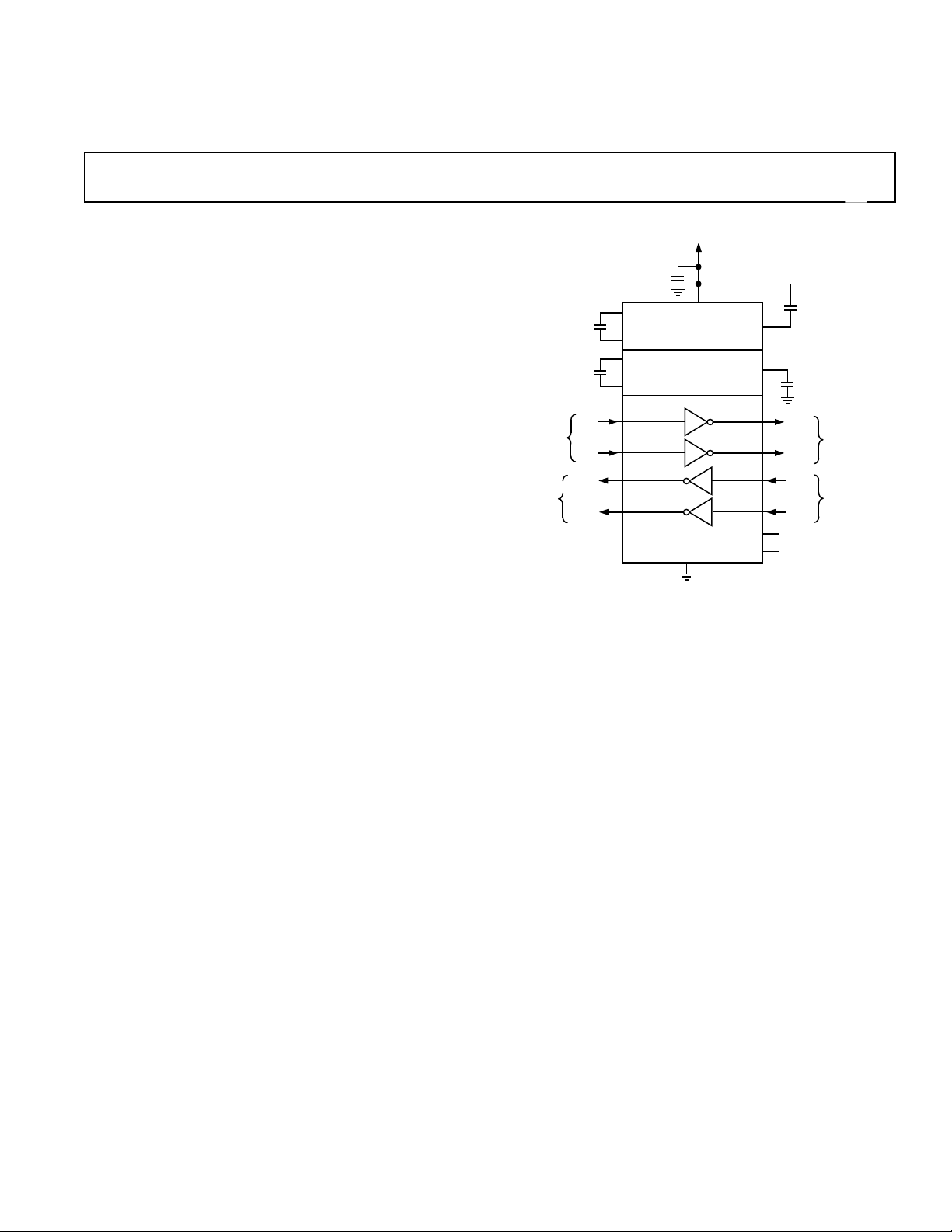
GENERAL DESCRIPTION
The ADM222, ADM232A, ADM242 are a family of high-speed
RS-232 line drivers/receivers offering transmission rates up to
200 kB/s. Operating from a single 5 V power supply, a highly
efficient on-chip charge pump using small (0.1 µF) external
capacitors allows RS-232 bipolar levels to be developed. Two
RS-232 drivers and two RS-232 receivers are provided on
each device.
The devices are fabricated on BiCMOS, an advanced mixed
technology process that combines low power CMOS with highspeed bipolar circuitry. This allows for transmission rates up to
200 kB/s, yet minimizes the quiescent power supply current to
under 5 mA.
The ADM232A is a pin-compatible, high-speed upgrade for the
AD232 and for the ADM232L. It is available in 16-lead DIP
and in both narrow and wide surface-mount (SOIC) packages.
The ADM222 contains an additional shutdown (SHDN) function that may be used to disable the device, thereby reducing the
supply current to 0.1 µA. During shutdown, all transmit/receive
CMOS RS-232 Drivers/Receivers
ADM222/ADM232A/ADM242
FUNCTIONAL BLOCK DIAGRAM
5V INPUT
0.1F
V
CC
+5V TO +10V
+5V TO –10V
T1
T2
R1
R2
GND
*
ON EACH TTL/CMOS INPUT
**
ON EACH RS-232 INPUT
V+
V–
EN
SHDN
INTERNAL 400k PULL-UP RESISTOR
INTERNAL 5k PULL-DOWN RESISTOR
TTL/CMOS
INPUTS
TTL/CMOS
OUTPUTS
*
0.1F
0.1F
T1
T2
R1
R2
OUT
OUT
C1+
VOLTAGE DOUBLER
C1–
C2+
VOLTAGE INVERTER
C2–
IN
IN
ADM2xx
functions are disabled. The ADM222 is available in 18-lead
DIP and in a wide surface-mount (SOIC) package.
The ADM242 combines both shutdown (SHDN) and enable
(EN) functions. The shutdown function reduces the supply
c
urrent to 0.1 mA. During shutdown, the transmitters are disabled but the receivers continue to operate normally. The
enable function allows the receiver outputs to be disabled
thereby facilitating sharing a common bus. The ADM242 is
available in 18-lead DIP and in a wide surface-mount (SOIC)
package.
0.1F
0.1F
T1
OUT
RS-232
OUTPUTS
T2
OUT
R1
IN
RS-232
INPUTS
R2
IN
(ADM242)
(ADM222, ADM242)
**
REV.
Information furnished by Analog Devices is believed to be accurate and
reliable. However, no responsibility is assumed by Analog Devices for its
use, nor for any infringements of patents or other rights of third parties
which may result from its use. No license is granted by implication or
otherwise under any patent or patent rights of Analog Devices.
One Technology Way, P.O. Box 9106, Norwood, MA 02062-9106, U.S.A.
Tel: 781/329-4700 World Wide Web Site: http://www.analog.com
Fax: © Analog Devices, Inc.,

(VCC = 5 V 10%. C1–C4 = 0.1 F; all spec-
B
ADM222/ADM232A/ADM242–SPECIFICATIONS
ifications T
MIN
to T
unless otherwise noted.)
MAX
Parameter Min Typ Max Unit Test Conditions/Comments
RS-232 TRANSMITTERS
Output Voltage Swing ± 5 ± 9 V All Transmitter Outputs Loaded with
3 kΩ to Ground
Input Logic Threshold Low, V
Input Logic Threshold High, V
INL
INH
2.4 1.7 V T
Logic Pull-Up Current 12 40 µAT
1.7 0.8 V T
IN
IN
= 0 V
IN
Data Rate 200 kB/s
Output Resistance 300 Ω V
= V+ = V– = 0 V, V
CC
OUT
= ± 2 V
Output Short Circuit Current (Instantaneous) ± 10 mA
RS-232 RECEIVERS
RS-232 Input Voltage Range –30 +30 V
RS-232 Input Threshold Low 0.8 1.2 V
RS-232 Input Threshold High 1.6 2.4 V
RS-232 Input Hysteresis 0.2 0.4 1.0 V V
RS-232 Input Resistance 3 5 7 kΩ T
TTL/CMOS Output Voltage Low, V
TTL/CMOS Output Voltage High, V
OL
OH
3.5 V I
0.05 0.4 V I
TTL/CMOS Output Short-Circuit Current –2 –85 mA Source Current (V
TTL/CMOS Output Short-Circuit Current 10 35 mA Sink Current (V
TTL/CMOS Output Leakage Current ± 0.05 ± 10 µA SHDN = GND/EN = V
EN Input Threshold Low, V
INL
EN Input Threshold High, V
INH
2.0 1.4 V
1.4 0.8 V
= 5 V
CC
= 0°C to 85°C
A
= 3.2 mA
OUT
= –1.0 mA
OUT
0 V ≤ V
OUT
≤ V
OUT
CC
= GND)*
OUT
= VCC)*
CC
POWER SUPPLY
Power Supply Current 4 8 mA No Load
13 mA 3 kΩ Load on Both Outputs
Shutdown Power Supply Current 0.1 10 µA
SHDN Input Leakage Current ± 1 µA
SHDN Input Threshold Low, V
INL
SHDN Input Threshold High, V
INH
2.0 1.4 V
1.4 0.8 V
AC CHARACTERISTICS
Transition Region Slew Rate 3 8 30 V/µsCL = 50 pF to 1000 pF, RL = 3 kΩ to 7 kΩ
Measured from +3 V to –3 V or –3 V to +3 V
Transmitter Propagation Delay TTL to RS-232 0.85 3.5 µst
1.0 3.5 µst
Receiver Propagation Delay RS-232 to TTL 0.1 0.5 µst
0.3 0.5 µst
Receiver Output Enable Time 125 500 ns t
Receiver Output Disable Time 160 500 ns t
PHLT
PLHT
PHLR
PLHR
ER
DR
Transmitter Output Enable Time 250 µs SHDN Goes High
Transmitter Output Disable Time 3.5 µs SHDN Goes Low
Transmitter + to – Propagation Delay Difference 150 ns
Receiver + to – Propagation Delay Difference 200 ns
*Guaranteed by design, not production tested.
Specifications subject to change without notice.
–2–
REV.
ADM222/ADM232A/ADM242
B
ABSOLUTE MAXIMUM RATINGS*
(TA = 25°C unless otherwise noted)
VCC . . . . . . . . . . . . . . . . . . . . . . . . . . . . . . . . . . . . . . . . . . 6 V
V+ . . . . . . . . . . . . . . . . . . . . . . . . . . . (V
– 0.3 V) to +13 V
CC
V– . . . . . . . . . . . . . . . . . . . . . . . . . . . . . . . . . +0.3 V to –13 V
Input Voltages
T
. . . . . . . . . . . . . . . . . . . . . . . . –0.3 V to (VCC + 0.3 V)
IN
R
. . . . . . . . . . . . . . . . . . . . . . . . . . . . . . . . . . . . . ± 30 V
IN
Output Voltages
T
. . . . . . . . . . . . . . . . . . . (V+, +0.3 V) to (V–, –0.3 V)
OUT
R
. . . . . . . . . . . . . . . . . . . . . . . –0.3 V to (VCC + 0.3 V)
OUT
Short Circuit Duration
T
. . . . . . . . . . . . . . . . . . . . . . . . . . . . . . . . Continuous
OUT
Power Dissipation N-16 . . . . . . . . . . . . . . . . . . . . . . 400 mW
(Derate 7.5 mW/°C above 70°C)
θ
, Thermal Impedance . . . . . . . . . . . . . . . . . . . . 80°C/W
JA
Power Dissipation R-16N . . . . . . . . . . . . . . . . . . . . . 400 mW
(Derate 7 mW/°C above 70°C)
θ
, Thermal Impedance . . . . . . . . . . . . . . . . . . . . 80°C/W
JA
Power Dissipation R-16W . . . . . . . . . . . . . . . . . . . . . 400 mW
(Derate 7 mW/°C above 70°C)
θ
, Thermal Impedance . . . . . . . . . . . . . . . . . . . . 80°CW
JA
Power Dissipation N-18 . . . . . . . . . . . . . . . . . . . . . . 400 mW
(Derate 7 mW/°C above 70°C)
θ
, Thermal Impedance . . . . . . . . . . . . . . . . . . . . 80°C/W
JA
Power Dissipation R-18W . . . . . . . . . . . . . . . . . . . . . 400 mW
(Derate 7 mW/°C above 70°C)
θ
, Thermal Impedance . . . . . . . . . . . . . . . . . . . . 80°C/W
JA
Operating Temperature Range
Industrial (A Version) . . . . . . . . . . . . . . . –40°C to +85°C
Storage Temperature Range . . . . . . . . . . . . –65°C to +150°C
Lead Temperature (Soldering, 10 sec) . . . . . . . . . . . . 300°C
Vapor Phase (60 sec) . . . . . . . . . . . . . . . . . . . . . . . . 215°C
Infrared (15 sec) . . . . . . . . . . . . . . . . . . . . . . . . . . . . . 220°C
*This is a stress rating only and functional operation of the device at these or any
other conditions above those indicated in the operation sections of this specification is not implied. Exposure to absolute maximum rating conditions for extended
periods of time may affect reliability.
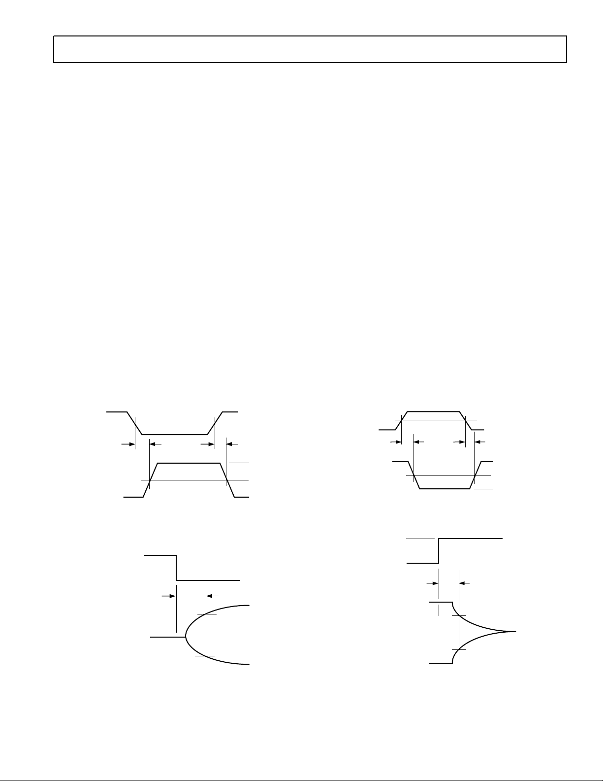
Test Circuits
V
IN
t
PLHT
V
OUT
Figure 1. Transmitter Propagation Delay Timing
3V
EN
INPUT
RECEIVER
OUTPUT
Figure 2. Receiver Enable Timing
t
PHLT
0V
t
ER
3.5V
0.8V
3V
V+
0V
V–
V
IN
t
PHLR
V
OUT
3V
0V
t
PLHR
V
CC
50%
GND
Figure 3. Receiver Propagation Delay Timing
3V
EN
INPUT
0V
t
DR
V
OH
V
– 0.5V
OH
RECEIVER
OUTPUT
VOL + 0.5V
V
OL
Figure 4. Receiver Disable Timing
REV.
–3–
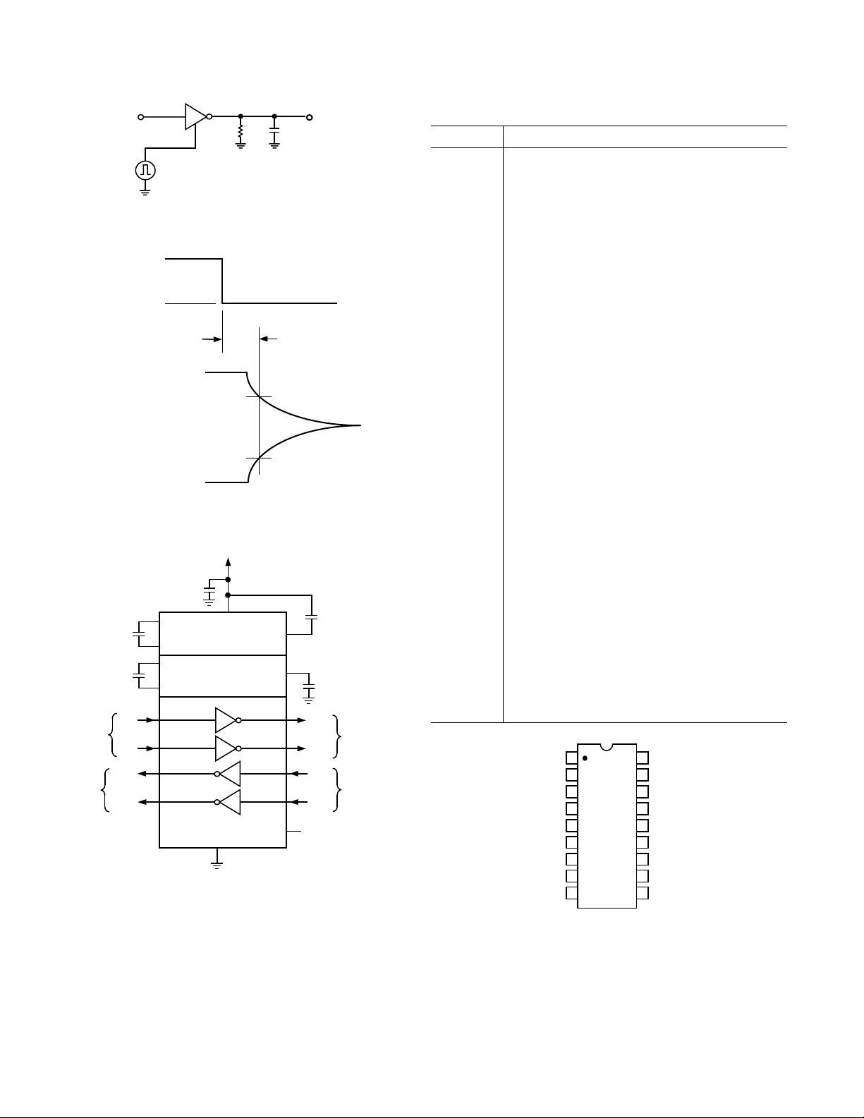
ADM222/ADM232A/ADM242
B
V
IN
SHDN
3k
50pF
Figure 5. Shutdown Test Circuit
3V
SHDN
INPUT
0V
t
DT
V+
+ 5V
TRANSMITTER
OUTPUT
– 5V
V–
Figure 6. Transmitter Shutdown Disable Timing
5V INPUT
C5
0.1F
TTL/CMOS
INPUTS
TTL/CMOS
OUTPUTS
*
0.1F
0.1F
T1
T2
R1
R2
C1
C2
OUT
OUT
6.3V
2
C1+
VOLTAGE DOUBLER
4
C1–
5
C2+
VOLTAGE INVERTER
6
C2–
12
IN
11
IN
13
10
ADM222
17
V
CC
+5V TO +10V
+5V TO –10V
T1
T2
R1
R2
GND
16
*
INTERNAL 400k PULL-UP RESISTOR
ON EACH TTL/CMOS INPUT
**
INTERNAL 5k PULL-DOWN RESISTOR
ON EACH RS-232 INPUT
3
V+
7
V–
15
T1
8
T2
14
R1
9
R2
18
SHDN
Figure 7. ADM222 Typical Operating Circuit
V
OUT
C3
0.1F
C4
0.1F
OUT
OUT
IN
IN
RS-232
OUTPUTS
RS-232
INPUTS
**
PIN FUNCTION DESCRIPTION
Mnemonic Function
V
CC
Power Supply Input, 5 V ± 10%.
V+ Internally generated positive supply (+10 V
nominal).
V– Internally generated negative supply (–10 V
nominal).
GND Ground Pin. Must be connected to 0 V.
C1+ External capacitor 1, (+ terminal) is connected
to this pin.
C1– External capacitor 1, (– terminal) is connected
to this pin.
C2+ External capacitor 2, (+ terminal) is connected
to this pin.
C2– External capacitor 2, (– terminal) is connected
to this pin.
T
IN
Transmitter (Driver) Inputs. These inputs accept
TTL/CMOS levels. An internal 400 kΩ pull-up
T
OUT
resistor to V
Transmitter (Driver) Outputs. These are RS-232
is connected on each input.
CC
levels (typically ±9 V).
R
IN
Receiver Inputs. These inputs accept RS-232
signal levels. An internal 5 kΩ pull-down resistor
to GND is connected on each of these inputs.
R
OUT
Receiver Outputs. These are TTL/CMOS levels.
NC No Connect. No connections are required to
this pin.
EN (ADM242 Only) Active Low Digital Input. May
be used to enable or disable (three-state) both
receiver outputs.
SHDN (ADM222 and ADM242) Active Low Digital
Input. May be used to disable the device so that
the power consumption is minimized. On the
ADM222 all drivers and receivers are disabled.
On the ADM242 the drivers are disabled but the
receivers remain enabled.
1
NC
2
C1+
V+
3
C1–
4
C2+
5
C2–
6
V–
7
T2
8
OUT
R2
9
IN
NC = NO CONNECT
ADM222
TOP VIEW
(Not to Scale)
18
SHDN
V
17
CC
GND
16
T1
15
OUT
R1
14
IN
R1
13
OUT
T1
12
IN
T2
11
IN
R2
10
OUT
Figure 8. ADM222 DIP and SOIC Pin Configurations
–4–
REV.

ADM222/ADM232A/ADM242
B
T2
C1+
V+
C1–
C2+
C2–
V–
OUT
R2
1
2
3
4
5
6
7
8
IN
ADM232A
TOP VIEW
(Not to Scale)
16
V
CC
GND
15
14
T1
OUT
13
R1
IN
R1
12
OUT
T1
11
IN
T2
10
IN
R2
9
OUT
Figure 9. ADM232A DIP/SOIC Pin Configuration
5V INPUT
C5
0.1F
TTL/CMOS
INPUTS
TTL/CMOS
OUTPUTS
*
0.1F
0.1F
T1
T2
R1
R2
C1
C2
OUT
OUT
6.3V
1
C1+
VOLTAGE DOUBLER
3
C1–
4
C2+
VOLTAGE INVERTER
5
C2–
11
IN
10
IN
12
9
16
V
CC
+5V TO +10V
+5V TO –10V
T1
T2
R1
R2
2
V+
6
V–
14
T1
7
T2
13
R1
8
R2
ADM232A
GND
15
*
INTERNAL 400k PULL-UP RESISTOR
ON EACH TTL/CMOS INPUT
**
INTERNAL 5k PULL-DOWN RESISTOR
ON EACH RS-232 INPUT
Figure 10. ADM232A Typical Operating Circuit
C3
0.1F
C4
0.1F
OUT
OUT
IN
IN
RS-232
OUTPUTS
RS-232
INPUTS
**
T2
EN
C1+
V+
C1–
C2+
C2–
V–
OUT
R2
1
2
3
4
5
6
7
8
9
IN
ADM242
TOP VIEW
(Not to Scale)
18
SHDN
V
17
CC
GND
16
T1
15
OUT
R1
14
IN
R1
13
OUT
T1
12
IN
T2
11
IN
R2
10
OUT
Figure 11. ADM242 DIP/SOIC Pin Configuration
5V INPUT
C5
0.1F
TTL/CMOS
INPUTS
TTL/CMOS
OUTPUTS
6.3V
2
C1+
VOLTAGE DOUBLER
4
C1–
5
C2+
VOLTAGE INVERTER
6
C2–
12
IN
11
IN
13
OUT
10
OUT
1
EN SHDN
0.1F
*
0.1F
C2
T1
T2
R1
R2
C1
17
V
CC
+5V TO +10V
+5V TO –10V
T1
T2
R1
R2
ADM242
GND
16
*
INTERNAL 400k PULL-UP RESISTOR
ON EACH TTL/CMOS INPUT
**
INTERNAL 5k PULL-DOWN RESISTOR
ON EACH RS-232 INPUT
3
V+
7
V–
15
T1
8
T2
14
9
18
Figure 12. ADM242 Typical Operating Circuit
C4
0.1F
R1
R2
C3
0.1F
OUT
OUT
IN
IN
RS-232
OUTPUTS
RS-232
INPUTS
**
REV.
–5–

ADM222/ADM232A/ADM242
B
–Typical Performance Characteristics
15
10
5
0
V+, V– – V
–5
–10
–15
05
V–
10 15 20 25 30
LOAD CURRENT – mA
V+
TPC 1. Charge Pump V+, V– vs. Current
9
7
5
3
1
–1
–3
–5
TRANSMITTER OUTPUT VOLTAGE – V
–7
–9
0 500
1000 1500 2000 2500 3000
LOAD CAPACITANCE – pF
115kBps
230kBps
115kBps
460kBps
460kBps
230kBps
TPC 2. Transmitter Baud Rate vs. Load Capacitance
15
10
5
0
–5
Tx O/P VOLTAGE – V
–10
–15
02
4681012
LOAD CURRENT – mA
Tx O/P HI
Tx O/P LO
14
TPC 4. Transmitter Output Voltage vs. Current
0.010V
A4
100
90
10
0%
5V 5V
100s
TPC 5. Charge Pump V+, V– Exiting Shutdown
T
: 6.2V
: 140ns
@: –3.5V
T
CH1 10.0V CH2 5.00V M 1.00s CH2 –6.4V
TPC 3. Transmitter Unloaded Slew Rate
–6–
T
: 6.0V
: 600ns
@: –2.9V
T
CH1 10.0V CH2 5.00V M 1.00s CH2 –6.4V
TPC 6. Transmitter Fully Loaded Slew Rate
REV.

ADM222/ADM232A/ADM242
B
GENERAL INFORMATION
The ADM222/ADM232A/ADM242 are high-speed RS-232
drivers/receivers requiring a single digital 5 V supply. The RS-232
standard requires transmitters that will deliver ±5 V minimum
on the transmission channel and receivers that can accept signal
levels down to ± 3 V. The parts achieve this by integrating stepup voltage converters and level-shifting transmitters and receivers
onto the same chip. CMOS technology is used to keep the
power dissipation to an absolute minimum. All devices contain an internal charge pump voltage doubler and a voltage
inverter that generates ± 10 V from the 5 V input. Four external 0.1 µF capacitors are required for the internal charge pump
voltage converter.
The ADM222/ADM232A/ADM242 is a modification, enhancement and improvement to the AD230-AD241 family and
derivatives thereof. It is essentially plug-in-compatible and does
not have materially different applications.
CIRCUIT DESCRIPTION
The internal circuitry consists of four main sections. These are:
Charge Pump Voltage Converter
TTL/CMOS to RS-232 Transmitters
RS-232 to TTL/CMOS Receivers
Enable and Shutdown Functions.
Charge Pump DC-DC Voltage Converter
The Charge Pump Voltage converter consists of an oscillator
and a switching matrix. The converter generates a ±10 V supply
from the input 5 V level. This is done in two stages using a
switched capacitor technique. The 5 V input supply is doubled
to 10 V using capacitor C1 as the charge storage element. The
–10 V level is also generated from the input 5 V supply using C1
and C2 as the storage elements.
Capacitors C3 and C4 are used to reduce the output ripple.
Their values are not critical and can be reduced if higher levels
of ripple are acceptable. The charge pump capacitors C1 and
C2 may also be reduced at the expense of higher output impedance on the V+ and V– supplies.
The V+ and V– supplies may also be used to power external
circuitry if the current requirements are small. Please refer to
the typical performance characteristics which shows the V+, V–
output voltage vs. current.
In the shutdown mode the charge pump is disabled and V+
decays to V
Transmitter (Driver) Section
while V– decays to 0 V.
CC
The Drivers convert TTL/CMOS input levels into RS-232
output levels. With V
= 5 V and driving a typical RS-232
CC
load, the output voltage swing is ±9 V. Even under worst-case
conditions the drivers are guaranteed to meet the ±5 V RS-232
minimum requirement.
The input threshold levels are both TTL- and CMOS-compatible with the switching threshold set at V
V
= 5 V, the switching threshold is 1.25 V typical. Unused
CC
/4. With a nominal
CC
inputs may be left unconnected, as an internal 400 kΩ pull-up
resistor pulls them high forcing the outputs into a low state.
As required by the RS-232 standard, the slew rate is limited to
less than 30 V/µs without the need for an external slew limiting
capacitor, and the output impedance in the power-off state is
greater than 300 Ω.
Receiver Section
The receivers are inverting level-shifters that accept RS-232
input levels (±3 V to ± 15 V) and translate them into 5 V TTL/
CMOS levels. The inputs have internal 5 kΩ pull-down resistors
to ground and are also protected against overvoltages of up to
± 30 V. The guaranteed switching thresholds are 0.8 V minimum and 2.4 V maximum, which are well within the ±3 V
RS-232 requirement. The low level threshold is deliberately
positive as it ensures that an unconnected input will be interpreted as a low level.
The receivers have Schmitt trigger input with a hysteresis level
of 0.5 V. This ensures error-free reception for both noisy inputs
and for inputs with slow transition times
Enable and Shutdown Functions
On the ADM222, both receivers are fully disabled during
shutdown.
On the ADM242, both receivers continue to operate normally.
This function is useful for monitoring activity so that when it
occurs, the device can be taken out of the shutdown mode.
The ADM242 also contains a receiver enable function (EN)
which can be used to fully disable the receivers, independent
of SHDN.
APPLICATIONS INFORMATION
A selection of typical operating circuits is shown in TPCs 1–6
and Figure 13.
2.0V
A1
100
90
10
0%
5V
5V
s
5
Figure 13. Transmitter Output Disable Timing
REV.
–7–

ADM222/ADM232A/ADM242
C
OUTLINE DIMENSIONS
0.800 (20.32)
0.790 (20.07)
0.780 (19.81)
16
1
0.100 (2.54)
BSC
0.210 (5.33)
MAX
0.150 (3.81)
0.130 (3.30)
0.115 (2.92)
0.022 (0.56)
0.018 (0.46)
0.014 (0.36)
0.070 (1.78)
0.060 (1.52)
0.045 (1.14)
CONTROLLING DIMENSIONS ARE IN INCHES; MILLIMETER DIMENSIONS
(IN PARENTHESES) ARE ROUNDED-OFF INCH EQUIVALENTS FOR
REFERENCE ON LY AND ARE NO T APPRO P RIATE FOR USE IN DESIGN.
CORNER LEADS MAY BE CONFIGURED AS WHOLE OR HALF LE ADS .
Figure 14. 16-Lead Plastic Dual In-Line Package [PDIP]
10.50 (0.4134)
10.10 (0.3976)
9
0.280 (7.11)
0.250 (6.35)
0.240 (6.10)
8
0.060 (1.52)
0.015
(0.38)
0.015 (0.38)
MIN
SEATING
PLANE
0.005 (0.13)
MIN
COMPLIANT TO JE DE C STANDARDS MS-001- AB
GAUGE
PLANE
MAX
0.325 (8.26)
0.310 (7.87)
0.300 (7.62)
0.430 (10.92)
MAX
Narrow Body
(N-16)
Dimensions shown in inches and (millimeters)
0.195 (4.95)
0.130 (3.30)
0.115 (2.92)
0.014 (0.36)
0.010 (0.25)
0.008 (0.20)
073106-B
0.30 (0.0 118)
0.10 (0.0039)
OPLANARITY
0.10
BSC
9
7.60 (0.2992)
7.40 (0.2913)
8
10.65 (0.4193)
10.00 (0.3937)
2.65 (0.1043)
2.35 (0.0925)
SEATING
PLANE
8°
0°
0.33 (0.0130)
0.20 (0.0079)
5
0
.
7
0
.
2
5
16
1
1.27 (0.0500)
0.51 (0.0201)
0.31 (0.0122)
CONTROLL ING DIMENSIONS ARE IN MILLIMETERS; INCH DIMENSIONS
(IN PARENTHESES) ARE ROUNDED-OFF MILLI M E TER EQUIVALENTS FOR
REFERENCE ON LY AND ARE NO T APPRO P RIATE FOR USE IN DESIGN.
COMPLIANT TO JEDE C STANDARDS MS-013-AA
Figure 15. 16-Lead Standard Small Outline Package [SOIC_W]
Wide Body
(RW-16)
Dimensions shown in millimeters and (inches)
(
0
.
0
2
9
0
0
9
(
0
.
1.27 (0.0500)
0.40 (0.0157)
5
)
45°
8
)
032707-B
–8–REV.B

ADM222/ADM232A/ADM242
4.00 (0.1575)
3.80 (0.1496)
0.25 (0.0098)
0.10 (0.0039)
COPLANARITY
0.10
CONTROLLING DIMENSIONSARE IN MILLIMETERS; INCH DI M E NS IONS
(IN PARENTHESES) ARE ROUNDED-OFF MILLI M E TER EQUIVALENTS FOR
REFERENCE ONLY AND ARE NOT APPRO P RIATE FOR USE IN DESIGN.
10.00 (0.3937)
9.80 (0.3858)
16
1
1.27 (0.0500)
BSC
0.51 (0.0201)
0.31 (0.0122)
COMPLIANT TO JEDEC STANDARDS MS-012-AC
9
6.20 (0.2441)
5.80 (0.2283)
8
1.75 (0.0689)
1.35 (0.0531)
SEATING
PLANE
0.25 (0.0098)
0.17 (0.0067)
0.50 (0.0197)
0.25 (0.0098)
8°
0°
1.27 (0.0500)
0.40 (0.0157)
45°
060606-A
Figure 16. 16-Lead Standard Small Outline Package [SOIC_N]
Narrow Body
(R-16)
Dimensions shown in millimeters and (inches)
11.75 (0.4626)
11.35 (0.4469)
18
1
10
7.60 (0.2992)
7.40 (0.2913)
9
10.65 (0.4193)
10.00 (0.3937)
0.30 (0.0118)
0.10 (0.0039)
COPLANARITY
0.10
0
.
7
0
.
2.65 (0.1043)
2.35 (0.0925)
(0.0500)
CONTROLL ING DIMENSIONS ARE IN MILLIMETERS; INCH DIMENSIONS
(IN PARENTHESES) ARE ROUNDED-OF F MI LLIMETER EQ UIVALENTS FOR
REFERENCE ON LY AND ARE NO T APPRO P RIATE FOR USE IN DESIGN.
0.31 (0.0122)
BSC
COMPLIANT TO JE DE C S TANDARDS MS-013-AB
0.51 (0.0201)
1.27
SEATING
PLANE
8°
0°
0.33 (0.0130)
0.20 (0.0079)
2
Figure 17. 18-Lead Standard Small Outline Package [SOIC_W]
Wide Body
(RW-18)
Dimensions shown in millimeters and (inches)
0
.
5
(
5
(
0
.
0
2
9
5
)
45°
0
9
8
)
0
1.27 (0.0500)
0.40 (0.0157)
060706-A
REV.B –9–

ADM222/ADM232A/ADM242
0.210 (5.33)
MAX
0.150 (3.81)
0.130 (3.30)
0.115 (2.92)
0.022 (0.56)
0.018 (0.46)
0.014 (0.36)
0.920 (23.37)
0.900 (22.86)
0.880 (22.35)
18
1
0.100 (2.54)
BSC
0.070 (1.78)
0.060 (1.52)
0.045 (1.14)
10
9
0.280 (7. 11)
0.250 (6.35)
0.240 (6.10)
0.015
(0.38)
MIN
SEATING
PLANE
0.005 (0.13)
MIN
0.060 (1.52)
MAX
0.015 (0.38)
GAUGE
PLANE
0.325 (8.26)
0.310 (7.87)
0.300 (7.62)
0.430 (10.92)
MAX
0.195 (4.95)
0.130 (3.30)
0.115 (2.92)
0.014 (0.36)
0.010 (0.25)
0.008 (0.20)
CONTROLL ING DIMENSIONS ARE IN INCHES; MILLIMETE R DI MENSIONS
(IN PARENTHESES) ARE ROUNDED-OFF INCH EQUIVALENTS FOR
REFERENCE ON LY AND ARE NO T APPRO P RIATE FOR USE IN DESIGN.
CORNER LEADS M AY BE CONFI GURED AS WHO LE OR HALF LEADS.
COMPLIANT TO JE DEC STANDARDS MS-001
070706-A
Figure 18. 18-Lead Plastic Dual In-Line Package [PDIP]
row B
Nar
ody
(N-18)
Dimensions shown in inches and (millimeters)
ORDERING GUIDE
Model1 Temperature Range Package Description Package Option
ADM222AN −40°C to +85°C 18-Lead PDIP N-18
ADM222ANZ −40°C to +85°C 18-Lead PDIP N-18
ADM222AR −40°C to +85°C 18-Lead SOIC_W RW-18
ADM222ARZ −40°C to +85°C 18-Lead SOIC_W RW-18
ADM222ARZ-REEL −40°C to +85°C 18-Lead SOIC_W RW-18
ADM232AAN −40°C to +85°C 16-Lead PDIP N-16
ADM232AANZ −40°C to +85°C 16-Lead PDIP N-16
ADM232AARN −40°C to +85°C 16-Lead SOIC_N R-16
ADM232AARN-REEL −40°C to +85°C 16-Lead SOIC_N R-16
ADM232AARN-REEL7 −40°C to +85°C 16-Lead SOIC_N R-16
ADM232AARNZ −40°C to +85°C 16-Lead SOIC_N R-16
ADM232AARNZ-REEL −40°C to +85°C 16-Lead SOIC_N R-16
ADM232AARNZ-REEL7 −40°C to +85°C 16-Lead SOIC_N R-16
ADM232AARW −40°C to +85°C 16-Lead SOIC_W RW-16
ADM232AARW-REEL −40°C to +85°C 16-Lead SOIC_W RW-16
ADM232AARWZ −40°C to +85°C 16-Lead SOIC_W RW-16
ADM232AARWZ-REEL −40°C to +85°C 16-Lead SOIC_W RW-16
ADM242AN −40°C to +85°C 18-Lead PDIP N-18
ADM242ANZ −40°C to +85°C 18-Lead PDIP N-18
ADM242AR −40°C to +85°C 18-Lead SOIC_W RW-18
ADM242AR-REEL −40°C to +85°C 18-Lead SOIC_W RW-18
ADM242ARZ −40°C to +85°C 18-Lead SOIC_W RW-18
ADM242ARZ-REEL −40°C to +85°C 18-Lead SOIC_W RW-18
1
Z = RoHS Compliant Part.
–10–REV.B

ADM222/ADM232A/ADM242
REVISION HISTORY
11/10—Rev. A to Rev. B
Updated Outline Dimensions ......................................................... 9
Changes to Ordering Guide .......................................................... 10
©2010 Analog Devices, Inc. All rights reserved. Trademarks and
registered trademarks are the property of their respective owners.
D01213-0-11/10(B)
REV.B –11–
 Loading...