

T
www.BDTIC.com/ADI
5 V-Powered
ADM231L–ADM234L/ADM236L–ADM241L
CMOS RS-232 Drivers/Receivers
FEATURES
Single 5 V power supply
Meets all EIA-232-E and V.28 specifications
120 kbps data rate
On-board dc-to-dc converters
±9 V output swing with 5 V supply
Small 1 µF capacitors
Low power shutdown ≤1 µA
±30 V receiver input levels
Latch-up free
APPLICATIONS
Computers
Peripherals
Modems
Printers
Instruments
GENERAL DESCRIPTION
The ADM2xx family of line drivers/receivers is intended for all
ADM236L TYPICAL OPERATING CIRCUIT
+5V INPUT
R1
R2
R3
ADM236L
V
CC
V+
V–
TL/CMOS
INPUTS
TTL/CMOS
OUTPUTS
C1+
C1–
C2+
C2–
+5V TO +10V
VOLTAGE
DOUBLER
+10V TO –10V
VOLTAGE
INVERTER
T1
T2
T3
T4
GND
1µF
+6.3V
1µF
+16V
T1
IN
T2
IN
1
T3
IN
T4
IN
R1
OUT
R2
OUT
R3
OUT
EN
1µF
+6.3V
1µF
+16V
T1
OUT
T2
OUT
T3
OUT
T4
OUT
R1
IN
R2
IN
R3
IN
SD
RS-232
OUTPUTS
RS-232
INPUTS
EIA-232-E and V.28 communications interfaces, especially in
1
applications in which 12 V is not available. The ADM236L and
ADM241L feature a low power shutdown mode that reduces
power dissipation to less than 5 µW, making them ideally suited
for battery-powered equipment. The ADM233L does not
require any external components and is particularly useful in
applications where printed circuit board space is critical.
All members of the ADM2xxL family, except the ADM231L and
ADM239L, include two internal charge pump voltage converters
that allow operation from a single 5 V supply. These parts convert
the 5 V input power to the ±10 V required for RS-232 output
levels. The ADM231L and ADM239L are designed to operate
from 5 V and 12 V supplies. An internal +12 V to −12 V charge
pump voltage converter generates the −12 V supply.
The ADM2xxL is an enhanced upgrade to the AD2xx family. It
features lower power consumption, faster slew rate, and the
ability to operate with smaller (1 µF) capacitors.
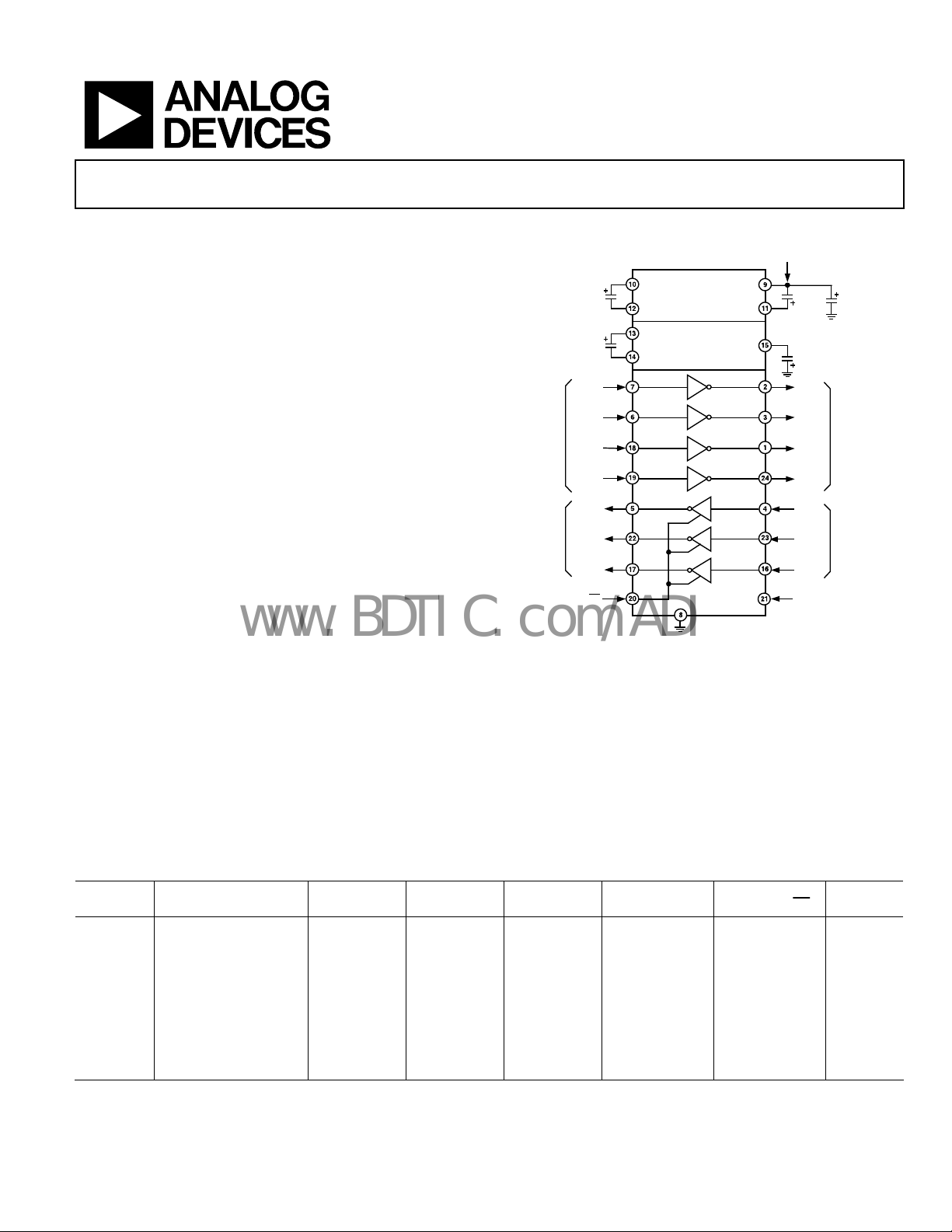
INTERNAL 400kΩ PULL-UP RESISTOR ON EACH TTL/CMOS INPUT.
2
INTERNAL 5kΩ PULL-DOWN RESISTOR ON EACH RS-232 INPUT.
Figure 1.
Table 1. Selection Table
Part
Number
Power Supply Voltage
No. of RS-232
Drivers
No. of RS-232
Receivers
External
Capacitors
Low Power
Shutdown (SD)
ADM231L 5 V and 7.5 V to 13.2 V 2 2 2 No No 14
ADM232L 5 V 2 2 4 No No 16
ADM233L 5 V 2 2 None No No 20
ADM234L 5 V 4 0 4 No No 16
ADM236L 5 V 4 3 4 Yes Yes 24
ADM237L 5 V 5 3 4 No No 24
ADM238L 5 V 4 4 4 No No 24
ADM239L 5 V and 7.5 V to 13.2 V 3 5 2 No Yes 24
ADM241L 5 V 4 5 4 Yes Yes 28
Rev. C
Information furnished by Analog Devices is believed to be accurate and reliable.
However, no responsibility is assumed by Analog Devices for its use, nor for any
infringements of patents or other rights of third parties that may result from its use.
Specifications subject to change without notice. No license is granted by implication
or otherwise under any patent or patent rights of Analog Devices. Trademarks and
registered trademarks are the property of their respective owners.
One Technology Way, P.O. Box 9106, Norwood, MA 02062-9106, U.S.A.
Tel: 781.329.4700 www.analog.com
Fax: 781.461.3113 © 2005 Analog Devices, Inc. All rights reserved.
TTL
Three-State
EN
No. of
Pins
1µF
+6.3V
2
00070-0-015

ADM231L–ADM234L/ADM236L–ADM241L
www.BDTIC.com/ADI
TABLE OF CONTENTS
Specifications..................................................................................... 3
General Information...................................................................... 12
Absolute Maximum Ratings............................................................ 4
ESD Caution.................................................................................. 4
Pin Configurations and Function Descriptions ........................... 5
Typical Performance Characteristics ............................................. 8
Typical Operating Circuits .............................................................. 9
REVISION HISTORY
4/05—Rev. B to Rev. C
Updated Format..................................................................Universal
Removed ADM223, ADM230L, and ADM235L............Universal
Changed Hysteresis Level..................................................Universal
Changes to Specifications Table...................................................... 3
Updated Outline Dimensions....................................................... 14
Changes to Ordering Guide.......................................................... 17
5/01—Rev. A to Rev. B
Edits to Test Conditions/Comments of Specifications................ 2
1/01—Rev. 0 to Rev. A
Removed ESD information from Features section ...................... 1
Changes to Specifications Table...................................................... 2
Removed ESD information from
Absolute Maximum Ratings section .............................................. 2
Circuit Description .................................................................... 12
Application Hints ....................................................................... 13
Outline Dimensions....................................................................... 14
Ordering Guide .......................................................................... 17
Revision 0: Initial Version
Rev. C | Page 2 of 20
ADM231L–ADM234L/ADM236L–ADM241L
www.BDTIC.com/ADI
SPECIFICATIONS
VCC = 5 V ± 10% (ADM231L, ADM232L, ADM234L, ADM236L, ADM238L, ADM239L, ADM241L); VCC = 5 V ± 5% (ADM233L and
ADM237L); V+ = 7.5 V to 13.2 V (ADM231L and ADM239L); C1 to C4 = 1.0 µF ceramic. All specifications T
MIN
to T
otherwise noted.
Table 2.
Parameter Min Typ Max Unit Test Conditions/Comments
Output Voltage Swing ±5 ±9 V
All transmitter outputs loaded with 3 kΩ to ground
VCC Power Supply Current 2.5 6.0 mA No load, (ADM232L only)
3.5 13 mA No load
V+ Power Supply Current 1.5 4 mA No load, V+ = 12 V (ADM231L and ADM239L only)
Shutdown Supply Current 1 10 µA
Input Logic Threshold Low, V
Input Logic Threshold High, V
0.8 V
INL
2.0 V
INH
, EN, SD, EN, SD
T
IN
, EN, SD, EN, SD
T
IN
Logic Pull-Up Current 12 25 µA
RS-232 Input Voltage Range1 –30 +30 V TIN = 0 V
RS-232 Input Threshold Low 0.8 1.2 V
RS-232 Input Threshold High 1.6 2.4 V
RS-232 Input Hysteresis 0.65 V
RS-232 Input Resistance 3 5 7 kΩ TA = 0°C to 85°C
TTL/CMOS Output Voltage Low, VOL 0.4 V
TTL/CMOS Output Voltage High, VOH 3.5 V I
TTL/CMOS Output Leakage Current +0.05 ±10 µA
= −1.0 mA
OUT
= VCC, 0 V ≤ R
EN
OUT
≤ VCC
Output Enable Time (TEN) 250 ns ADM236L, ADM239L, ADM241L (Figure 31, CL = 150 pF)
Output Disable Time (T
50 ns ADM236L, ADM239L, ADM241L (Figure 31, RL = 1 kΩ)
DIS)
Propagation Delay 0.3 µs RS-232 to TTL
Transition Region Slew Rate 8 V/µs RL = 3 kΩ, CL = 2500 pF, measured from +3 V to −3 V or −3 V to +3 V
Output Resistance 300 Ω VCC = V+ = V– = 0 V, V
= ±2 V
OUT
RS-232 Output Short-Circuit Current ±10 mA
1
Guaranteed by design.
MAX
, unless
Rev. C | Page 3 of 20
ADM231L–ADM234L/ADM236L–ADM241L
www.BDTIC.com/ADI
ABSOLUTE MAXIMUM RATINGS
TA = 25°C, unless otherwise noted.
Table 3.
Parameter Rating
VCC –0.3 V to +6 V
V+ (VCC – 0.3 V) to +14 V
V– +0.3 V to −14 V
Input Voltages
TIN –0.3 V to (VCC + 0.3 V)
RIN ±30 V
Output Voltages
T
(V+, +0.3 V) to (V–, –0.3 V)
OUT
R
–0.3 V to (VCC + 0.3 V)
OUT
Short-Circuit Duration
T
Continuous
OUT
Power Dissipation
N-14 PDIP (Derate 10 mW/°C
above 70°C)
N-16 PDIP (Derate 10.5 mW/°C
above 70°C)
N-20 PDIP (Derate 11 mW/°C
above 70°C)
N-24-1 PDIP (Derate
13.5 mW/°C above 70°C)
R-16 SOIC (Derate 9 mW/°C
above 70°C)
R-24 SOIC (Derate 12 mW/°C
above 70°C)
R-28 SOIC (Derate 12.5 mW/°C
above 70°C)
RS-28 SSOP (Derate 10 mW/°C
above 70°C)
800 mW
840 mW
890 mW
1000 mW
760 mW
850 mW
900 mW
900 mW
Parameter Rating
Q-14 CERDIP (Derate 10 mW/°C
above 70°C)
Q-16 CERDIP (Derate 10 mW/°C
above 70•C)
Q-24 CERDIP (Derate
12.5 mW/°C above 70°C)
Thermal Impedance, θJA
N-14 PDIP 140°C/W
N-16 PDIP 135°C/W
N-20 PDIP 125°C/W
N-24-1 PDIP 120°C/W
R-16 SOIC 105°C/W
R-24 SOIC 85°C/W
R-28 SOIC 80°C/W
RS-28 SSOP 100°C/W
Q-14 CERDIP 105°C/W
Q-16 CERDIP 100°C/W
Q-24 CERDIP 55°C/W
Operating Temperature Range
Commercial (J Version) 0°C to 70°C
Industrial (A Version) −40°C to +85°C
Storage Temperature Range −65°C to +150°C
Lead Temperature, Soldering 300°C
Vapor Phase (60 sec) 215°C
Infrared (15 sec) 220° C
720 mW
800 mW
1000 mW
Stresses above those listed under Absolute Maximum Ratings
may cause permanent damage to the device. This is a stress
rating only and functional operation of the device at these or
any other conditions above those indicated in the operational
sections of this specification is not implied. Exposure to
absolute maximum rating conditions for extended periods of
time may affect device reliability.
ESD CAUTION
ESD (electrostatic discharge) sensitive device. Electrostatic charges as high as 4000 V readily accumulate on
the human body and test equipment and can discharge without detection. Although this product features
proprietary ESD protection circuitry, permanent damage may occur on devices subjected to high energy
electrostatic discharges. Therefore, proper ESD precautions are recommended to avoid performance
degradation or loss of functionality.
Rev. C | Page 4 of 20
ADM231L–ADM234L/ADM236L–ADM241L
T
T
T
www.BDTIC.com/ADI
PIN CONFIGURATIONS AND FUNCTION DESCRIPTIONS
14
C1+
1
–
C1
2
–
3
V
T2
OUT
R2
R2
OUT
T2
IN
IN
4
(Not to Scale)
5
6
7
ADM231L
TOP VIEW
V+
13
V
CC
12
GND
11
T1
OUT
10
R1
IN
9
R1
OUT
8
T1
IN
Figure 2. ADM231L PDIP Pin Configuration
C1+
1
C1–
2
3
V–
T2
OUT
R2
R2
OUT
T2
NC
ADM231L
4
5
(Not to Scale)
IN
6
7
IN
8
NC = NO CONNECT
TOP VIEW
16
V+
V
15
CC
14
GND
T1
13
OUT
R1
12
IN
R1
11
OUT
T1
10
IN
9
NC
Figure 3. ADM231L SOIC Pin Configuration
00070-0-004
00070-0-037
T2
1
IN
T1
2
IN
R1
3
OUT
R1
4
IN
5
6
7
8
9
10
ADM233L
TOP VIEW
(Not to Scale)
T1
OUT
GND C2+
V
CC
C1+
GND
C2–
R2
20
OUT
R2
19
IN
T2
18
OUT
V–
17
C2–
16
15
V+
14
C1–
13
V–
12
C2+
11
00070-0-008
Figure 5. ADM233L PDIP Pin Configuration
1
OUT
2
OUT
T2
T1
GND
V
C1+
CC
V+
IN
IN
1
2
3
4
5
(Not to Scale)
6
7
8
ADM234L
TOP VIEW
T3
16
OUT
T4
15
OUT
T4
14
IN
T3
13
IN
V–
12
C2–
11
C2+
10
C1–
9
00070-0-010
Figure 6. ADM234L PDIP/CERDIP/SOIC Pin Configuration
V
16
CC
GND
15
T1
14
OUT
R1
13
IN
R1
12
OUT
T1
11
IN
10
T2
IN
R2
9
OUT
00070-0-006
2
R2
C1+
C1–
C2+
C2–
OUT
1
V+
2
3
ADM232L
4
TOP VIEW
5
(Not to Scale)
V–
6
7
8
IN
Figure 4. ADM232L PDIP/CERDIP/SOIC Pin Configuration
Rev. C | Page 5 of 20
T3
T1
T2
R1
OUT
OUT
OUT
R1
OUT
T2
T1
GND
V
C1+
V+
C1–
IN
IN
IN
CC
1
2
3
4
5
6
7
8
9
10
11
12
ADM236L
TOP VIEW
(Not to Scale)
T4
24
OUT
R2
23
IN
R2
22
OUT
SD
21
20
EN
T4
19
IN
T3
18
IN
R3
17
OUT
R3
16
IN
V–
15
C–
14
C2+
13
00070-0-014
Figure 7. ADM236L PDIP/SOIC Pin Configuration
ADM231L–ADM234L/ADM236L–ADM241L
www.BDTIC.com/ADI
R1
T3
T1
T2
OUT
OUT
OUT
R1
OUT
T2
T1
GND
V
C1–
IN
IN
CC
V+
IN
1
2
3
4
5
6
7
8
9
10
11
12
ADM237L
TOP VIEW
(Not to Scale)
T4
24
OUT
R2
23
IN
R2
22
OUT
T5
21
IN
T5
20
OUT
T4
19
IN
T3
18
IN
R3
17
OUT
R3
16
IN
V–C1+
15
C2–
14
C2+
13
00070-0-016
Figure 8. ADM237L PDIP/CERDIP/SOIC Pin Configuration
T2
1
OUT
T1
2
OUT
R2
3
IN
R2
4
OUT
T1
5
IN
R1
OUT
R1
GND
V
CC
IN
6
7
(Not to Scale)
8
9
ADM238L
TOP VIEW
10
V+
11
C1– C2+
12
T3
24
OUT
R3
23
IN
R3
22
OUT
T4
21
IN
T4
20
OUT
T3
19
IN
T2
18
IN
R4
17
OUT
R4
16
IN
V–C1+
15
C2–
14
13
00070-0-018
Figure 9. ADM238L PDIP/CERDIP/SOIC Pin Configuration
R1
1
OUT
R1
2
IN
3
GND
V
4
CC
V+
5
IN
IN
6
7
8
9
10
11
12
ADM239L
TOP VIEW
(Not to Scale)
C+
C–
V–
R5
R5
OUT
R4
OUT
R4
T1
24
IN
T2
23
IN
R2
22
OUT
R2
21
IN
20
T2
OUT
T1
19
OUT
R3
18
IN
R3
17
OUT
T3
16
IN
NC
15
14
EN
T3
13
OUT
00070-0-020
Figure 10. ADM239L PDIP/CERDIP/SOIC Pin Configuration
T3
1
OUT
T1
2
OUT
T2
3
OUT
R2
4
R2
5
OUT
T2
6
IN
T1
7
ADM241L
IN
R1
OUT
R1
IN
GND
V
CC
C1+
V+
C1–
8
9
10
11
12
13
14
TOP VIEW
(Not to Scale)
T4
28
OUT
R3
27
IN
R3
26
OUT
25
SD
OUT
24
EN
R4
23
IN
R4
22
OUT
T4
21
IN
T3
20
IN
R5
19
OUT
R5
18
IN
V–
17
16
C2–
15
C2+
00070-0-022
Figure 11. ADM241L SOIC/SSOP Pin Configuration
Rev. C | Page 6 of 20

ADM231L–ADM234L/ADM236L–ADM241L
www.BDTIC.com/ADI
Table 4. Pin Function Descriptions
Mnemonic Function
VCC Power Supply Input. 5 V ± 10% (5 V ± 5% for ADM233L).
V+
V− Internally Generated Negative Supply (−10 V nominal).
GND Ground Pin. Must be connected to 0 V.
C+ (ADM231L and ADM239L only) External capacitor (+ terminal) is connected to this pin.
C− (ADM231L and ADM239L only) External capacitor (– terminal) is connected to this pin.
C1+
Internally Generated Positive Supply (+10 V nominal) on all parts, except ADM231L and ADM239L. ADM231L and ADM239L
require an external 7.5 V to 13.2 V supply.
(ADM232L, ADM234L, ADM236L, ADM237L, ADM238L, and ADM241L) External capacitor (+ terminal) is connected to this
pin. (ADM233L) The capacitor is connected internally and no external connection to this pin is required.
C1−
C2+
C2−
TIN
T
OUT
RIN Receiver Inputs. These inputs accept RS-232 signal levels. An internal 5 kΩ pull-down resistor to GND is connected on each input.
R
Receiver Outputs. These are TTL/CMOS levels.
OUT
EN
SD
NC No Connect. No connections are required to this pin.
Table 5. ADM236L and ADM241L Truth Table
SD
0 0 Normal Operation Enabled Enabled
0 1 Normal Operation Enabled Disabled
1 0 Shutdown Disabled Disabled
(ADM232L, ADM234L, ADM236L, ADM237L, ADM238L, and ADM241L) External capacitor (− terminal) is connected to this
pin. (ADM233L) The capacitor is connected internally and no external connection to this pin is required.
(ADM232L, ADM234L, ADM236L, ADM237L, ADM238L, and ADM241L) External capacitor (+ terminal) is connected to this
pin. (ADM233L) Internal capacitor connections, Pin 11 and Pin 15, must be connected together.
(ADM232L, ADM234L, ADM236L, ADM237L, ADM238L, and ADM241L) External capacitor (− terminal) is connected to this
pin. (ADM233L) Internal capacitor connections, Pin 10 and Pin 16, must be connected together.
Transmitter (Driver) Inputs. These inputs accept TTL/CMOS levels. An internal 400 kΩ pull-up resistor to VCC is connected to
each input.
Transmitter (Driver) Outputs. These are RS-232 levels (typically ±10 V).
Enable Input. Active low on ADM236L, ADM239L, and ADM241L. This input is used to enable/disable the receiver outputs.
With EN
= low, the receiver outputs are enabled. With EN = high, the outputs are placed in a high impedance state. This
facility is useful for connecting to microprocessor systems.
Shutdown Input. Active high on ADM236L and ADM241L. With SD = high on the ADM236L and ADM241L, the charge pump
is disabled, the receiver outputs are placed in a high impedance state, and the driver outputs are turned off.
EN
Status Transmitters T1 to T5 Receivers R1 to R5
Rev. C | Page 7 of 20

ADM231L–ADM234L/ADM236L–ADM241L
www.BDTIC.com/ADI
TYPICAL PERFORMANCE CHARACTERISTICS
15
10
5
0
V+/V– (V)
–5
–10
–15
0
V+
V–
510
LOAD CURRENT (mA)
Figure 12. Charge Pump V+ and V− vs. Current
50
45
40
35
s)
µ
30
25
20
SLEW RATE (V/
15
10
5
0
POSITIVE
SLEW
0 500
NEGATIVE
SLEW
1000
LOAD CAPACITANCE (pF)
1500 2000 2500 3000
Figure 13. Transmitter Slew Rate vs. Load Capacitance
15
10
5
0
Tx O/P (V)
–5
–10
15
20
00070-0-026
–15
0
Tx O/P HI
Tx O/P LO
48
LOAD CURRENT (mA)
62
10
00070-0-029
Figure 15. Transmitter Output Voltage vs. Current
350
00070-0-027
300
250
200
150
IMPEDANCE (Ω)
100
50
0
4.5 4.7
V+ IMP
V– IMP
4.9 5.1 5.3 5.5
VCC(V)
Figure 16. Charge Pump Impedance vs. V
00070-0-030
CC
9
7
5
3
1
–1
Tx O/P (V)
–3
–5
–7
–9
4.0 4.5
Tx O/P HI LOADED
Tx O/P LO LOADED
5.0 5.5 6.0
V
(V)
CC
Figure 14. Transmitter Output Voltage vs. V
00070-0-028
CC
Rev. C | Page 8 of 20

ADM231L–ADM234L/ADM236L–ADM241L
T
S
T
www.BDTIC.com/ADI
TYPICAL OPERATING CIRCUITS
+5V INPUT
1µF
+5V INPUT
13
V
CC
V+
V–
R1
R2
TTL/CMOS
INPUTS
TTL/CMOS
OUTPUTS
1
2
8
7
9
6
C1+
C1–
GND
+12V TO –12V
VOLTAGE
INVERTER
T1
T2
ADM231L
12
1µF
+16V
T1
IN
1
T2
IN
R1
OUT
R2
OUT
1
INTERNAL 400kΩ PULL-UP RESISTOR ON EACH TTL/CMOS INPUT.
2
INTERNAL 5kΩ PULL-DOWN RESISTOR ON EACH RS-232 INPUT.
Figure 17. ADM231L Typical Operating Circuit (PDIP Pinout)
R1
R2
ADM232L
V
CC
V+
V–
TTL/CMOS
INPUTS
TL/CMO
OUTPUTS
C1+
C1–
C2+
C2–
+5V TO +10V
VOLTAGE
DOUBLER
+10V TO –10V
VOLTAGE
INVERTER
T1
T2
1µF
+6.3V
1µF
+16V
T1
IN
1
T2
IN
R1
OUT
R2
OUT
GND
14
3
11
4
10
5
5V INPUT
+7.5V TO +13.2V
1µF
+16V
T1
OUT
RS-232
OUTPUTS
T2
OUT
R1
IN
RS-232
INPUTS
R2
IN
1µF
1µF
+6.3V
+6.3V
1µF
+16V
T1
OUT
RS-232
OUTPUTS
T2
OUT
R1
IN
RS-232
INPUTS
R2
IN
V
T1
TTL/CMOS
INPUTS
TTL/CMOS
OUTPUTS
DO NOT MAKE
CONNECTIONS TO
2
THESE PINS
–10V POWER
00070-0-005
+10V POWER
1
2
IN
1
T2
IN
R1
OUT
R2
OUT
C1+
C1–
INTERNAL
SUPPLY
INTERNAL
SUPPLY
INTERNAL 400kΩ PULL-UP RESISTOR ON EACH TTL/CMOS INPUT.
INTERNAL 5kΩ PULL-DOWN RESISTOR ON EACH RS-232 INPUT.
V–
V–
V+
CC
T1
T2
R1
R2
ADM233L
GND
GND
C2+
C2+
C2–
C2–
T1
OUT
RS-232
OUTPUTS
T2
OUT
R1
IN
RS-232
2
INPUTS
R2
IN
00070-0-009
Figure 19. ADM233L Typical Operating Circuit
5V INPUT
1µF
+6.3V
1µF
+16V
T1
T2
T3
T4
OUT
OUT
OUT
OUT
1µF
+6.3V
RS-232
OUTPUTS
ADM234L
V
CC
V+
V–
C1+
C1–
C2+
C2–
GND
+5V TO +10V
VOLTAGE
DOUBLER
+10V TO –10V
VOLTAGE
INVERTER
T1
T2
T3
T4
1µF
+6.3V
1µF
+16V
T1
IN
T2
TL/CMOS
INPUTS
2
IN
1
T3
IN
T4
IN
1
INTERNAL 400kΩ PULL-UP RESISTOR ON EACH TTL/CMOS INPUT.
2
INTERNAL 5kΩ PULL-DOWN RESISTOR ON EACH RS-232 INPUT.
00070-0-007
Figure 18. ADM232L Typical Operating Circuit
Rev. C | Page 9 of 20
1
INTERNAL 400kΩ PULL-UP RESISTOR ON EACH TTL/CMOS INPUT.
00070-0-011
Figure 20. ADM234L Typical Operating Circuit

ADM231L–ADM234L/ADM236L–ADM241L
T
T
T
www.BDTIC.com/ADI
+5V INPUT
+5V INPUT
TL/CMOS
INPUTS
TTL/CMOS
OUTPUTS
R1
R2
R3
ADM236L
V
CC
V+
V–
SD
C1+
C1–
C2+
C2–
+5V TO +10V
VOLTAGE
DOUBLER
+10V TO –10V
VOLTAGE
INVERTER
T1
T2
T3
T4
GND
1µF
+6.3V
1µF
+16V
T1
IN
T2
IN
1
T3
IN
T4
IN
R1
OUT
R2
OUT
R3
OUT
EN
1
INTERNAL 400kΩ PULL-UP RESISTOR ON EACH TTL/CMOS INPUT.
2
INTERNAL 5kΩ PULL-DOWN RESISTOR ON EACH RS-232 INPUT.
Figure 21. ADM236L Typical Operating Circuit
1µF
+6.3V
1µF
+16V
T1
OUT
T2
OUT
T3
OUT
T4
OUT
R1
IN
R2
IN
R3
IN
1µF
+6.3V
RS-232
OUTPUTS
RS-232
INPUTS
R1
R2
R3
R4
ADM238L
V
CC
V+
V–
1µF
+6.3V
1µF
+16V
T1
OUT
T2
OUT
T3
OUT
T4
OUT
R1
IN
R2
IN
R3
IN
R4
IN
1µF
+6.3V
RS-232
OUTPUTS
RS-232
INPUTS
2
00070-0-019
C1+
C1–
C2+
C2–
+5V TO +10V
VOLTAGE
DOUBLER
+10V TO –10V
VOLTAGE
INVERTER
T1
T2
T3
T4
GND
1µF
+6.3V
1µF
+16V
T1
IN
T2
TL/CMOS
INPUTS
2
00070-0-015
TTL/CMOS
OUTPUTS
IN
1
T3
IN
T4
IN
R1
OUT
R2
OUT
R3
OUT
R4
OUT
1
INTERNAL 400kΩ PULL-UP RESISTOR ON EACH TTL/CMOS INPUT.
2
INTERNAL 5kΩ PULL-DOWN RESISTOR ON EACH RS-232 INPUT.
Figure 23. ADM238L Typical Operating Circuit
TL/CMOS
INPUTS
TTL/CMOS
OUTPUTS
+5V INPUT
R1
R2
R3
ADM237L
V
CC
V+
V–
T1
T2
T3
T4
20
T5
R1
R2
R3
C1+
C1–
C2+
C2–
+5V TO +10V
VOLTAGE
DOUBLER
+10V TO –10V
VOLTAGE
INVERTER
T1
T2
T3
T4
T5
1µF
+6.3V
1µF
+16V
T1
IN
T2
IN
T3
IN
1
T4
IN
T5
IN
R1
OUT
R2
OUT
R3
OUT
GND
1
INTERNAL 400kΩ PULL-UP RESISTOR ON EACH TTL/CMOS INPUT.
2
INTERNAL 5kΩ PULL-DOWN RESISTOR ON EACH RS-232 INPUT.
1µF
+6.3V
1µF
+16V
OUT
OUT
OUT
OUT
OUT
IN
IN
IN
1µF
+6.3V
RS-232
OUTPUTS
RS-232
INPUTS
2
00070-0-017
Figure 22. ADM237L Typical Operating Circuit
Rev. C | Page 10 of 20

ADM231L–ADM234L/ADM236L–ADM241L
T
www.BDTIC.com/ADI
TL/CMOS
INPUTS
TTL/CMOS
OUTPUTS
+5V INPUT
1µF
V
R1
R2
R3
R4
R5
ADM239L
CC
V+
V–
+7.5V TO +13.2V
INPUT
1µF
+16V
T1
OUT
RS-232
T2
OUT
OUTPUTS
T3
OUT
R1
IN
R2
IN
RS-232
R3
IN
INPUTS
R4
IN
R5
IN
NC
TTL/CMOS
INPUTS
2
TTL/CMOS
OUTPUTS
+12V TO –12V
1µF
+16V
T1
IN
T2
IN
1
T3
IN
R1
OUT
R2
OUT
R3
OUT
R4
OUT
R5
OUT
EN
C1+
C1–
VOLTAGE
INVERTER
T1
T2
T3
GND
1µF
+16V
1µF
+16V
T1
IN
T2
IN
1
T3
IN
T4
IN
R1
OUT
R2
OUT
R3
OUT
R4
OUT
R5
OUT
EN
C1+
C1–
C2+
C2–
+5V TO +10V
VOLTAGE
DOUBLER
+10V TO –10V
VOLTAGE
INVERTER
T1
T2
T3
T4
R1
R2
R3
R4
R5
ADM241L
GND
V
+5V INPUT
CC
V+
V–
1µF
+6.3V
1
µ
+16V
T1
OUT
T2
OUT
T3
OUT
T4
OUT
R1
IN
R2
IN
R3
IN
R4
IN
R5
IN
SD
F
1µF
+6.3V
RS-232
OUTPUTS
RS-232
INPUTS
2
1
INTERNAL 400kΩ PULL-UP RESISTOR ON EACH TTL/CMOS INPUT.
2
INTERNAL 5kΩ PULL-DOWN RESISTOR ON EACH RS-232 INPUT.
Figure 24. ADM239L Typical Operating Circuit
1
INTERNAL 400kΩ PULL-UP RESISTOR ON EACH TTL/CMOS INPUT.
2
00070-0-021
INTERNAL 5kΩ PULL-DOWN RESISTOR ON EACH RS-232 INPUT.
00070-0-023
Figure 25. ADM241L Typical Operating Circuit
Rev. C | Page 11 of 20

ADM231L–ADM234L/ADM236L–ADM241L
www.BDTIC.com/ADI
GENERAL INFORMATION
The ADM231L–ADM234L/ADM236L–ADM241L family of
RS-232 drivers/receivers is designed to solve interface problems
by meeting the EIA-232-E specifications while using a single
digital 5 V supply. The EIA-232-E standard requires that transmitters deliver ±5 V minimum on the transmission channel
and that receivers can accept signal levels down to ±3 V. The
ADM231L–ADM234L/ADM236L–ADM241L meet these
requirements by integrating step-up voltage converters and
level-shifting transmitters and receivers onto the same chip.
CMOS technology is used to keep the power dissipation to
an absolute minimum. A comprehensive range of transmitter/
receiver combinations is available for most communications needs.
The ADM236L and ADM241L are particularly useful in
battery-powered systems because they feature a low power
shutdown mode that reduces power dissipation to less than 5 µW.
The ADM233L is designed for applications in which space
saving is important because the charge pump capacitors are
molded into the package. The ADM231L and ADM239L
include only a negative charge pump converter and are intended
for applications in which +12 V is available.
To facilitate sharing a common line or for connection to a
microprocessor data bus, the ADM236L, ADM239L, and
ADM241L feature an enable (EN,
receivers are disabled, their outputs are placed in a high
impedance state.
1
CH1
CH3
Figure 26. Charge Pump V+ and V− Exiting Shutdown
1
2
5.00V CH2 5.00V M1.00
CH1
Figure 27. Transmitter Output Loaded Slew Rate
5.00V
5.00V
T
T
T
B
W
CH2 5.00V M50.0µs
V+, V– EXITING SD
) function. When the
EN
3.1V
CH1
Tx INPUT
T
T
Tx OUTPUT
µ
s CH1
800mV
SD
V+
V–
00070-0-031
00070-0-032
1
2
5.00V CH2 5.00V M1.00
CH1
T
T
µ
s CH1
800mV
Tx INPUT
Tx OUTPUT
00070-0-033
Figure 28. Transmitter Output Unloaded Slew Rate
CIRCUIT DESCRIPTION
The internal circuitry in the ADM236L to ADM241L consists of
three main sections: a charge pump voltage converter, RS-232-toTTL/CMOS receivers, and TTL/CMOS-to-RS-232 transmitters.
Charge Pump DC-to-DC Voltage Converter
The charge pump voltage converter consists of an oscillator and
a switching matrix. The converter generates a 10 V supply from
the 5 V input. This is done in two stages using a switched
capacitor technique, as illustrated in Figure 29 and Figure 30.
First, the 5 V input supply is doubled to 10 V, using capacitor
C1 as the charge storage element. The 10 V level is then
inverted to generate –10 V, using C2 as the storage element.
V
CC
GND
INTERNAL
OSCILLATOR
FROM
VOLTAGE
DOUBLER
INTERNAL
OSCILLATOR
Capacitors C3 and C4 are used to reduce the output ripple.
Their values are not critical and can be reduced if higher levels
of ripple are acceptable. The charge pump capacitors, C1 and C2,
can be reduced at the expense of higher output impedance on the
V+ and V– supplies, and the V+ and V– supplies can be used to
power external circuitry if the current requirements are small.
S1 S3
S2 S4
C1 C3
Figure 29. Charge Pump Voltage Doubler
S1 S3
+
V
S2 S4
GND
+
C2 C4
Figure 30. Charge Pump Voltage Inverter
V+ = 2V
CC
V
CC
GND
+
V– = –(V+)
00070-0-034
00070-0-035
Rev. C | Page 12 of 20

ADM231L–ADM234L/ADM236L–ADM241L
www.BDTIC.com/ADI
Transmitter (Driver) Section
The drivers convert TTL/CMOS input levels into EIA-232-E
output levels. With V
= +5 V and driving a typical EIA-232-E
CC
load, the output voltage swing is ±9 V. Even under worst-case
conditions, the drivers are guaranteed to meet the ±5 V
EIA-232-E minimum requirement.
The input threshold levels are both TTL- and CMOS-compatible
with the switching threshold set at V
/4. With a nominal VCC =
CC
5 V, the switching threshold is 1.25 V typical. Unused inputs can
be left unconnected because an internal 400 kΩ pull-up resistor
pulls them high, forcing the outputs into a low state.
As required by the EIA-232-E standard, the slew rate is limited to
less than 30 V/µs without the need for an external slew-limiting
capacitor, and the output impedance in the power-off state is
greater than 300 Ω.
Receiver Section
The receivers are inverting level shifters that accept EIA-232-E
input levels (±5 V to ±15 V) and translate them into 5 V TTL/
CMOS levels. The inputs have internal 5 kΩ pull-down resistors
to ground and are protected against overvoltages of up to ±30 V.
The guaranteed switching thresholds are 0.8 V minimum and
2.4 V maximum, which are well within the ±3 V EIA-232-E
requirement. The low level threshold is deliberately positive
because it ensures that an unconnected input is interpreted as
a low level.
The receivers have Schmitt trigger inputs with a hysteresis level
of 0.65 V. This ensures error-free reception for both noisy inputs
and inputs with slow transition times.
Shutdown (SD)
The ADM236L and ADM241L feature a control input that can
be used to disable the part and reduce the power consumption
to less than 5 µW. This is very useful in battery-operated systems.
During shutdown, the charge pump is turned off, the transmitters
are disabled, and all receivers are put into a high impedance,
disabled state. The shutdown control input is active high on all
parts (see Table 5).
Enable Input
ADM239L and ADM241L feature an enable input used to enable
or disable the receiver outputs. The enable input is active low on
the ADM239L and ADM241L (see Table 5). When the receivers
are disabled, their outputs are placed in a high impedance state.
This function allows the outputs to be connected directly to a
microprocessor data bus. It can also be used to allow receivers
from different devices to share a common data line. The timing
diagram for the enable function is shown in Figure 31.
3V
EN
0V
T
EN
R
OUT
3.5V
0.8V
Figure 31. Enable Timing
T
DIS
– 0.1V
V
OH
+ 0.1V
V
OL
APPLICATION HINTS
Driving Long Cables
In accordance with the EIA-232-E standard, long cables are permissible, provided that the total load capacitance does not exceed
2500 pF. For longer cables that do exceed this, it is possible to trade
off baud rate for cable length. Large load capacitances cause a
reduction in slew rate; therefore, the maximum transmission baud
rate is decreased. The ADM236L to ADM241L are designed to
minimize the slew rate reduction that occurs as load capacitance increases.
For the receivers, it is important that a high level of noise
immunity be built in so that slow rise and fall times do not
cause multiple output transitions as the signal passes slowly
through the transition region. The ADM236L to ADM241L
have 0.65 V of hysteresis to guard against this. This ensures that
even in noisy environments error-free reception can be
achieved.
High Baud Rate Operation
The ADM236L to ADM241L feature high slew rates, permitting
data transmission at rates well in excess of the EIA-232-E
specification. The drivers maintain ±5 V signal levels at data
rates up to 100 kbps under worst-case loading conditions.
00070-0-036
Rev. C | Page 13 of 20

ADM231L–ADM234L/ADM236L–ADM241L
C
R
N
www.BDTIC.com/ADI
OUTLINE DIMENSIONS
0.685 (17.40)
0.665 (16.89)
0.645 (16.38)
14
17
0.100 (2.54)
BSC
0.015 (0.38)
0.180 (4.57)
MAX
0.150 (3.81)
0.130 (3.30)
0.110 (2.79)
CONTROLLING DIMENSIONS ARE IN INCHES; MILLIMETER DIMENSIONS
(IN PARENTHESES) ARE ROUNDED-OFF INCH EQUIVALENTS FOR
REFERENCE ONLY AND ARE NOT APPROPRIATE FOR USE IN DESIGN
0.022 (0.56)
0.018 (0.46)
0.014 (0.36)
COMPLIANT TO JEDEC STANDARDS MO-095-AB
0.060 (1.52)
0.050 (1.27)
0.045 (1.14)
Figure 32. 14-Lead Plastic Dual In-Line Package [PDIP]
Dimensions shown in inches and (millimeters)
8
MIN
(N-14)
0.295 (7.49)
0.285 (7.24)
0.275 (6.99)
SEATING
PLANE
0.325 (8.26)
0.310 (7.87)
0.300 (7.62)
0.015 (0.38)
0.010 (0.25)
0.008 (0.20)
0.150 (3.81)
0.135 (3.43)
0.120 (3.05)
10.50 (0.4134)
10.10 (0.3976)
16
1
1.27 (0.0500)
BSC
0.30 (0.0118)
0.10 (0.0039)
COPLANARITY
0.10
CONTROLLING DIMENSIONS ARE IN MILLIMETERS; INCH DIMENSIONS
(IN PARENTHESES) ARE ROUNDED-OFF MILLIMETER EQUIVALENTS FOR
REFERENCE ONLY AND ARE NOT APPROPRIATE FOR USE IN DESIGN
0.51 (0.0201)
0.31 (0.0122)
COMPLIANT TO JEDEC STANDARDS MS-013AA
9
7.60 (0.2992)
7.40 (0.2913)
8
2.65 (0.1043)
2.35 (0.0925)
SEATING
PLANE
10.65 (0.4193)
10.00 (0.3937)
0.33 (0.0130)
0.20 (0.0079)
8°
0°
Figure 34. 16-Lead Standard Small Outline Package [SOIC]
Wide Body (R-16)
Dimensions shown in millimeters and (inches)
0.75 (0.0295)
0.25 (0.0098)
1.27 (0.0500)
0.40 (0.0157)
× 45°
0.785 (19.94)
0.765 (19.43)
0.745 (18.92)
16
1
0.100 (2.54)
BSC
0.015 (0.38)
0.180 (4.57)
MAX
0.150 (3.81)
0.130 (3.30)
0.110 (2.79)
0.022 (0.56)
0.018 (0.46)
0.014 (0.36)
CONTROLLING DIMENSIONS ARE IN INCHES; MILLIMETER DIMENSIONS
(IN PARENTHESES) ARE ROUNDED-OFF INCH EQUIVALENTS FOR
REFERENCE ONLY AND ARE NOT APPROPRIATE FOR USE IN DESIGN
COMPLIANT TO JEDEC STANDARDS MO-095AC
0.060 (1.52)
0.050 (1.27)
0.045 (1.14)
9
8
MIN
0.295 (7.49)
0.285 (7.24)
0.275 (6.99)
SEATING
PLANE
0.325 (8.26)
0.310 (7.87)
0.300 (7.62)
0.015 (0.38)
0.010 (0.25)
0.008 (0.20)
Figure 33. 16-Lead Plastic Dual In-Line Package [PDIP]
(N-16)
Dimensions shown in inches and (millimeters)
0.150 (3.81)
0.135 (3.43)
0.120 (3.05)
0.005 (0.13) MIN
PIN 1
0.200 (5.08)
0.200 (5.08)
0.125 (3.18)
ONTROLLING DIMENSIONS ARE IN INCHES; MILLIMETER DIMENSIONS
(IN PARENTHESES) ARE ROUNDED-OFF INCH EQUIVALENTS FO
REFERENCE ONLY AND ARE NOT APPROPRIATE FOR USE IN DESIG
0.785 (19.94) MAX
MAX
0.023 (0.58)
0.014 (0.36)
0.098 (2.49) MAX
14
17
0.100 (2.54) BSC
8
0.070 (1.78)
0.030 (0.76)
0.310 (7.87)
0.220 (5.59)
0.060 (1.52)
0.015 (0.38)
0.150
(3.81)
MIN
SEATING
PLANE
0.320 (8.13)
0.290 (7.37)
15°
0°
0.015 (0.38)
0.008 (0.20)
Figure 35. 14-Lead Ceramic Dual In-Line Package [CERDIP]
(Q-14)
Dimensions shown in inches and (millimeters)
Rev. C | Page 14 of 20

ADM231L–ADM234L/ADM236L–ADM241L
0
0
0
www.BDTIC.com/ADI
0.005
(0.13)
MIN
PIN 1
0.200 (5.08)
MAX
0.200 (5.08)
0.125 (3.18)
0.023 (0.58)
0.014 (0.36)
CONTROLLING DIMENSIONS ARE IN INCHES; MILLIMETER DIMENSIONS
(IN PARENTHESES) ARE ROUNDED-OFF INCH EQUIVALENTS FOR
REFERENCE ONLY AND ARE NOT APPROPRIATE FOR USE IN DESIGN
0.098 (2.49)
MAX
16
18
0.840 (21.34) MAX
0.100
0.070 (1.78)
(2.54)
0.030 (0.76)
BSC
9
0.310 (7.87)
0.220 (5.59)
0.060 (1.52)
0.015 (0.38)
0.150 (3.81)
MIN
SEATING
PLANE
Figure 36. 16-Lead Ceramic Dual In-Line Package [CERDIP]
(Q-16)
Dimensions shown in inches and (millimeters)
15°
0°
0.320 (8.13)
0.290 (7.37)
0.015 (0.38)
0.008 (0.20)
0.005
(0.13)
MIN
PIN 1
0.200 (5.08)
MAX
0.200 (5.08)
0.125 (3.18)
0.023 (0.58)
0.014 (0.36)
CONTROLLING DIMENSIONS ARE IN INCHES; MILLIMETER DIMENSIONS
(IN PARENTHESES) ARE ROUNDED-OFF INCH EQUIVALENTS FOR
REFERENCE ONLY AND ARE NOT APPROPRIATE FOR USE IN DESIGN
Figure 39. 20-Lead Ceramic Dual In-Line Package [CERDIP]
0.098 (2.49)
MAX
20
110
1.060 (26.92) MAX
0.100
0.070 (1.78)
(2.54)
0.030 (0.76)
BSC
11
0.310 (7.87)
0.220 (5.59)
0.060 (1.52)
0.015 (0.38)
0.150 (3.81)
MIN
SEATING
PLANE
(Q-20)
Dimensions shown in inches and (millimeters)
15°
0°
0.320 (8.13)
0.290 (7.37)
0.015 (0.38)
0.008 (0.20)
0.985 (25.02)
0.965 (24.51)
0.945 (24.00)
20
1
0.180 (4.57)
MAX
0.150 (3.81)
0.130 (3.30)
0.110 (2.79)
0.022 (0.56)
0.018 (0.46)
0.014 (0.36)
CONTROLLING DIMENSIONS ARE IN INCHES; MILLIMETER DIMENSIONS
(IN PARENTHESES) ARE ROUNDED-OFF INCH EQUIVALENTS FOR
REFERENCE ONLY AND ARE NOT APPROPRIATE FOR USE IN DESIGN
COMPLIANT TO JEDEC STANDARDS MO-095-AE
0.015 (0.38) MIN
0.100
0.060 (1.52)
(2.54)
0.050 (1.27)
BSC
0.045 (1.14)
0.295 (7.49)
0.285 (7.24)
0.275 (6.99)
11
10
SEATING
PLANE
0.325 (8.26)
0.310 (7.87)
0.300 (7.62)
Figure 37. 20-Lead Plastic Dual In-Line Package [PDIP]
(N-20)
Dimensions shown in inches and (millimeters)
13.00 (0.5118)
12.60 (0.4961)
20 11
1
0.30 (0.0118)
0.10 (0.0039)
1.27
COPLANARITY
0.10
COMPLIANT TO JEDEC STANDARDS MS-013AC
CONTROLLING DIMENSIONS ARE IN MILLIMETERS; INCH DIMENSIONS
(IN PARENTHESES) ARE ROUNDED-OFF MILLIMETER EQUIVALENTS FOR
REFERENCE ONLY AND ARE NOT APPROPRIATE FOR USE IN DESIGN
(0.0500)
BSC
0.51 (0.0201)
0.31 (0.0122)
7.60 (0.2992)
7.40 (0.2913)
10
2.65 (0.1043)
2.35 (0.0925)
SEATING
PLANE
10.65 (0.4193)
10.00 (0.3937)
0.33 (0.0130)
0.20 (0.0079)
8°
0°
Figure 38. 20-Lead Standard Small Outline Package [SOIC]
Wide Body (R-20)
Dimensions shown in millimeters and (inches)
0.015 (0.38)
0.010 (0.25)
0.008 (0.20)
0.75 (0.0295)
0.25 (0.0098)
0.150 (3.81)
0.135 (3.43)
0.120 (3.05)
× 45°
1.27 (0.0500)
0.40 (0.0157)
1.185 (30.01)
1.165 (29.59)
1.145 (29.08)
24
112
0.180
(4.57)
MAX
.150 (3.81)
.130 (3.30)
.110 (2.79)
0.022 (0.56)
0.018 (0.46)
0.014 (0.36)
CONTROLLING DIMENSIONS ARE IN INCHES; MILLIMETER DIMENSIONS
(IN PARENTHESES) ARE ROUNDED-OFF INCH EQUIVALENTS FOR
REFERENCE ONLY AND ARE NOT APPROPRIATE FOR USE IN DESIGN
0.100
(2.54)
BSC
COMPLIANT TO JEDEC STANDARDS MO-095AG
13
0.015 (0.38) MIN
0.060 (1.52)
0.050 (1.27)
0.045 (1.14)
0.295 (7.49)
0.285 (7.24)
0.275 (6.99)
SEATING
PLANE
0.325 (8.26)
0.310 (7.87)
0.300 (7.62)
0.015 (0.38)
0.010 (0.25)
0.008 (0.20)
0.150 (3.81)
0.135 (3.43)
0.120 (3.05)
Figure 40. 24-Lead Plastic Dual In-Line Package [PDIP]
(N-24-1)
Dimensions shown in inches and (millimeters)
BSC
0.098 (2.49) MAX
13
0.610 (15.49)
0.500 (12.70)
21
0.075 (1.91)
0.015 (0.38)
0.070 (1.78)
0.030 (0.76)
SEATING
PLANE
0.150
(3.81)
MIN
0.620 (15.75)
0.590 (14.99)
0.015 (0.38)
0.008 (0.20)
0.005 (0.13) MIN
24
PIN 1
0.023 (0.58)
0.014 (0.36)
1.290 (32.77) MAX
0.100 (2.54)
0.225 (5.72)
MAX
0.200 (5.08)
0.120 (3.05)
CONTROLLING DIMENSIONS ARE IN INCHES; MILLIMETER DIMENSIONS
(IN PARENTHESES) ARE ROUNDED-OFF INCH EQUIVALENTS FOR
REFERENCE ONLY AND ARE NOT APPROPRIATE FOR USE IN DESIGN
Figure 41. 24-Lead Side-Brazed Ceramic Dual In-Line Package [SBDIP]
(D-24-2)
Dimensions shown in inches and (millimeters)
Rev. C | Page 15 of 20

ADM231L–ADM234L/ADM236L–ADM241L
0
Y
www.BDTIC.com/ADI
1.290 (32.77)
1.150 (31.57)
24
1
PIN 1
.210 (5.34)
MAX
0.200 (5.08)
0.115 (2.92)
0.022 (0.56)
0.018 (0.46)
0.014 (0.36)
CONTROLLING DIMENSIONS ARE IN INCHES; MILLIMETER DIMENSIONS
(IN PARENTHESES) ARE ROUNDED-OFF INCH EQUIVALENTS FOR
REFERENCE ONLY AND ARE NOT APPROPRIATE FOR USE IN DESIGN
0.100
(2.54)
BSC
COMPLIANT TO JEDEC STANDARDS MS-011-AA
Figure 42. 24-Lead Plastic Dual In-Line Package [PDIP]
Dimensions shown in inches and (millimeters)
13
0.580 (14.73)
0.485 (12.32)
12
0.015 (0.38) MIN
0.070 (1.78)
0.030 (0.76)
SEATING
PLANE
Wide Body (N-24-2)
0.610 (15.49)
0.600 (15.24)
0.590 (14.99)
0.015 (0.38)
0.010 (0.25)
0.008 (0.20)
0.165 (4.19)
0.160 (4.06)
0.155 (3.93)
18.10 (0.7126)
17.70 (0.6969)
28 15
1
0.30 (0.0118)
0.10 (0.0039)
COPLANARITY
0.10
1.27 (0.0500)
COMPLIANT TO JEDEC STANDARDS MS-013AE
CONTROLLING DIMENSIONS ARE IN MILLIMETERS; INCH DIMENSIONS
(IN PARENTHESES) ARE ROUNDED-OFF MILLIMETER EQUIVALENTS FOR
REFERENCE ONLY AND ARE NOT APPROPRIATE FOR USE IN DESIGN
BSC
0.51 (0.0201)
0.33 (0.0130)
14
2.65 (0.1043)
2.35 (0.0925)
SEATING
PLANE
7.60 (0.2992)
7.40 (0.2913)
10.65 (0.4193)
10.00 (0.3937)
0.33 (0.0130)
0.20 (0.0079)
0.75 (0.0295)
0.25 (0.0098)
8°
0°
× 45°
1.27 (0.0500)
0.40 (0.0157)
Figure 45. 28-Lead Standard Small Outline Package [SOIC]
Wide Body (R-28)
Dimensions shown in millimeters and (inches)
10.50
10.20
9.90
0.005 (0.13)
MIN
24
PIN 1
112
0.200 (5.08)
MAX
0.200 (5.08)
0.125 (3.18)
0.023 (0.58)
0.014 (0.36)
CONTROLLING DIMENSIONS ARE IN INCHES; MILLIMETER DIMENSIONS
(IN PARENTHESES) ARE ROUNDED-OFF INCH EQUIVALENTS FOR
REFERENCE ONLY AND ARE NOT APPROPRIATE FOR USE IN DESIGN
0.098 (2.49)
1.280 (32.51) MAX
0.100
(2.54)
BSC
MAX
13
0.070 (1.78)
0.030 (0.76)
0.310 (7.87)
0.220 (5.59)
0.060 (1.52)
0.015 (0.38)
0.150 (3.81)
MIN
SEATING
PLANE
Figure 43. 24-Lead Ceramic Dual in-Line Package [CERDIP]
(Q-24)
Dimensions shown in inches and (millimeters)
15.60 (0.6142)
15.20 (0.5984)
24 13
1
0.30 (0.0118)
0.10 (0.0039)
COPLANARIT
1.27 (0.0500)
0.10
COMPLIANT TO JEDEC STANDARDS MS-013AD
CONTROLLING DIMENSIONS ARE IN MILLIMETERS; INCH DIMENSIONS
(IN PARENTHESES) ARE ROUNDED-OFF MILLIMETER EQUIVALENTS FOR
REFERENCE ONLY AND ARE NOT APPROPRIATE FOR USE IN DESIGN
BSC
0.51 (0.020)
0.31 (0.012)
7.60 (0.2992)
7.40 (0.2913)
12
2.65 (0.1043)
2.35 (0.0925)
SEATING
PLANE
10.65 (0.4193)
10.00 (0.3937)
0.33 (0.0130)
0.20 (0.0079)
Figure 44. 24-Lead Standard Small Outline Package [SOIC]
Wide Body (R-24)
Dimensions shown in millimeters and (inches)
15°
0°
0.75 (0.0295)
0.25 (0.0098)
8°
0°
0.320 (8.13)
0.290 (7.37)
0.015 (0.38)
0.008 (0.20)
× 45°
1.27 (0.0500)
0.40 (0.0157)
28 15
5.60
8.20
5.30
7.80
5.00
7.40
COPLANARITY
0.10
0.25
0.09
8°
4°
0°
0.95
0.75
0.55
1.85
1.75
1.65
SEATING
PLANE
14
1
PIN 1
2.00 MAX
0.65
0.05 MIN
BSC
0.38
0.22
COMPLIANT TO JEDEC STANDARDS MO-150AH
Figure 46. 28-Lead Shrink Small Outline Package [SSOP]
(RS-28)
Dimensions shown in millimeters
Rev. C | Page 16 of 20

ADM231L–ADM234L/ADM236L–ADM241L
www.BDTIC.com/ADI
ORDERING GUIDE
Model Temperature Range Package Description Package Option
ADM231LJN 0°C to 70°C 14-lead PDIP N-14
ADM231LJR 0°C to 70°C 16-lead SOIC R-16
ADM231LJR-REEL 0°C to 70°C 16-lead SOIC R-16
ADM231LJRZ-REEL1 0°C to 70°C 16-lead SOIC R-16
ADM231LAN –40°C to +85°C 14-lead PDIP N-14
ADM231LAQ –40°C to +85°C 14-lead CERDIP Q-14
ADM231LAR –40°C to +85°C 16-lead SOIC R-16
ADM231LAR-REEL –40°C to +85°C 16-lead SOIC R-16
ADM232LJR 0°C to 70°C 16-lead SOIC R-16
ADM232LJR-REEL 0°C to 70°C 16-lead SOIC R-16
ADM232LJRZ1 0°C to 70°C 16-lead SOIC R-16
ADM232LJRZ-REEL71 0°C to 70°C 16-lead SOIC R-16
ADM232LAN –40°C to +85°C 16-lead PDIP N-16
ADM232LAR –40°C to +85°C 16-lead SOIC R-16
ADM232LAR-REEL –40°C to +85°C 16-lead SOIC R-16
ADM232LARZ1 –40°C to +85°C 16-lead SOIC R-16
ADM232LARZ-REEL1 –40°C to +85°C 16-lead SOIC R-16
ADM232LJN 0°C to 70°C 20-lead PDIP N-16
ADM232LJNZ1 0°C to 70°C 20-lead PDIP N-16
ADM233LJN 0°C to 70°C 20-lead PDIP N-20
ADM233LAN –40°C to +85°C 20-lead PDIP N-20
ADM234LJN 0°C to 70°C 16-lead PDIP N-16
ADM234LJR 0°C to 70°C 16-lead SOIC R-16
ADM234LJR-REEL 0°C to 70°C 16-lead SOIC R-16
ADM234LJRZ1 0°C to 70°C 16-lead SOIC R-16
ADM234LJRZ-REEL1 0°C to 70°C 16-lead SOIC R-16
ADM234LAN –40°C to +85°C 16-lead PDIP N-16
ADM234LAQ –40°C to +85°C 16-lead CERDIP Q-16
ADM234LAR –40°C to +85°C 16-lead SOIC R-16
ADM234LAR-REEL –40°C to +85°C 16-lead SOIC R-16
ADM236LJN 0°C to 70°C 24-lead PDIP N-24-1
ADM236LJR 0°C to 70°C 24-lead SOIC R-24
ADM236LJR-REEL 0°C to 70°C 24-lead SOIC R-24
ADM236LAN –40°C to +85°C 24-lead PDIP N-24-1
ADM236LAR –40°C to +85°C 24-lead SOIC R-24
ADM236LAR-REEL –40°C to +85°C 24-lead SOIC R-24
ADM237LJN 0°C to 70°C 24-lead PDIP N-24-1
ADM237LJR 0°C to 70°C 24-lead SOIC R-24
ADM237LJR-REEL 0°C to 70°C 24-lead SOIC R-24
ADM237LJRZ1 0°C to 70°C 24-lead SOIC R-24
ADM237LJRZ-REEL1 0°C to 70°C 24-lead SOIC R-24
ADM237LAN –40°C to +85°C 24-lead PDIP N-24-1
ADM237LAQ –40°C to +85°C 24-lead CERDIP Q-24
ADM237LAR –40°C to +85°C 24-lead SOIC R-24
ADM237LAR-REEL –40°C to +85°C 24-lead SOIC R-24
ADM238LJN 0°C to 70°C 24-lead PDIP N-24-1
ADM238LJNZ1 0°C to 70°C 24-lead PDIP N-24-1
ADM238LJR 0°C to 70°C 24-lead SOIC R-24
ADM238LJR-REEL 0°C to 70°C 24-lead SOIC R-24
ADM238LJRZ1 0°C to 70°C 24-lead SOIC R-24
ADM238LJRZ-REEL1 0°C to 70°C 24-lead SOIC R-24
Rev. C | Page 17 of 20

ADM231L–ADM234L/ADM236L–ADM241L
www.BDTIC.com/ADI
Model Temperature Range Package Description Package Option
ADM238LAN –40°C to +85°C 24-lead PDIP N-24-1
ADM238LAQ –40°C to +85°C 24-lead CERDIP Q-24
ADM238LAR –40°C to +85°C 24-lead SOIC R-24
ADM238LAR-REEL –40°C to +85°C 24-lead SOIC R-24
ADM238LARZ1 –40°C to +85°C 24-lead SOIC R-24
ADM238LARZ-REEL1 –40°C to +85°C 24-lead SOIC R-24
ADM239LJN 0°C to 70°C 24-lead PDIP N-24-1
ADM239LJR 0°C to 70°C 24-lead SOIC R-24
ADM239LJR-REEL 0°C to 70°C 24-lead SOIC R-24
ADM239LJRZ1 0°C to 70°C 24-lead SOIC R-24
ADM239LJRZ-REEL1 0°C to 70°C 24-lead SOIC R-24
ADM239LAN –40°C to +85°C 24-lead PDIP N-24-1
ADM239LAQ –40°C to +85°C 24-lead CERDIP Q-24
ADM239LAR –40°C to +85°C 24-lead SOIC R-24
ADM239LAR-REEL –40°C to +85°C 24-lead SOIC R-24
ADM241LJR 0°C to 70°C 28-lead SOIC R-28
ADM241LJR-REEL 0°C to 70°C 28-lead SOIC R-28
ADM241LJRZ1 0°C to 70°C 28-lead SOIC R-28
ADM241LJRZ-REEL1 0°C to 70°C 28-lead SOIC R-28
ADM241LAR –40°C to +85°C 28-lead SOIC R-28
ADM241LAR-REEL –40°C to +85°C 28-lead SOIC R-28
ADM241LJRS 0°C to 70°C 28-lead SSOP RS-28
ADM241LJRS-REEL 0°C to 70°C 28-lead SSOP RS-28
ADM241LARS –40°C to +85°C 28-lead SSOP RS-28
ADM241LARS-REEL –40°C to +85°C 28-lead SSOP RS-28
1
Z = Pb-free part.
Rev. C | Page 18 of 20

ADM231L–ADM234L/ADM236L–ADM241L
www.BDTIC.com/ADI
NOTES
Rev. C | Page 19 of 20

ADM231L–ADM234L/ADM236L–ADM241L
www.BDTIC.com/ADI
NOTES
© 2005 Analog Devices, Inc. All rights reserved. Trademarks and
registered trademarks are the property of their respective owners.
C00070–0–4/05(C)
Rev. C | Page 20 of 20
 Loading...