

Quad Voltage Up and Down Sequencer
V
www.BDTIC.com/ADI
and Monitor with Programmable Timing
FEATURES
Powered from 2.7 V to 5.5 V on the VCC pin
Monitors four supplies via 0.8% accurate comparators
Digital core supports up and down supply sequencing
Multiple devices can be cascaded (ADM1186-1)
Four inputs can be programmed to monitor different voltage
le
vels with resistor dividers
Capacitor programmable supply sequence time delays
and a tim
Four open-drain enable outputs
Open-drain power-good output
Open-drain sequence complete pin and bidirectional
open-
APPLICATIONS
Monitor and alarm functions
Up and down power supply sequencing
Telecommunication and data communication equipment
PCs, servers, and notebook PCs
eout delay to 5% accuracy at 25°C
drain fault pin (ADM1186-1 only)
ADM1186
GENERAL DESCRIPTION
The ADM1186-1 and ADM1186-2 are integrated, four-channel
voltage monitoring and sequencing devices. A 2.7 V to 5.5 V
power supply is required on the VCC pin for power.
Four precision comparators, VIN1 to VIN4, monitor four
age rails. All four comparators share a 0.6 V reference and
volt
have a worst-case accuracy of 0.8%. Resistor networks that are
external to the VIN1, VIN2, VIN3, and VIN4 pins set the
undervoltage (UV) trip points for the monitored supply rails.
The ADM1186-1 and ADM1186-2 have four open-drain enable
utputs, OUT1 to OUT4, that are used to enable power supplies.
o
An open-drain power-good output, PWRGD, indicates whether
the four VINx inputs are above their UV thresholds.
DO
A state machine monitors the state of the UP and
on the ADM1186-1 or the UP/
DOWN
pin on the ADM1186-2
to control the supply sequencing direction (see Figure 2). In the
AIT START state, a rising edge transition on the UP or
W
DOWN
UP/
transition on the
pin triggers a power-up sequence. A falling edge
DOWN
or UP/
DOWN
pin in the POWER-UP
DONE state triggers a power-down sequence.
WN
pins
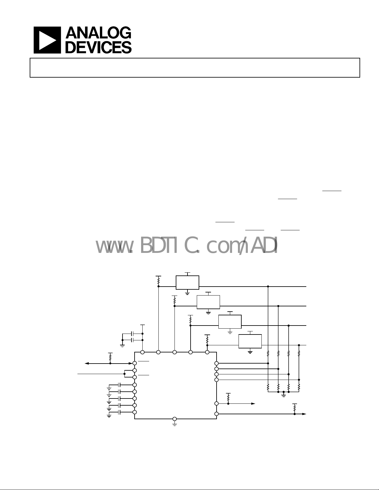
3.3V AUX
SEQUENCE CONTRO L
3.3V AUX
1µF
100nF
VCC OUT1 OUT2
FAU LT
UP
DOWN
DLY_EN_OUT1
DLY_EN_OUT2
DLY_EN_OUT3
DLY_EN_OUT4
BLANK_DLY
APPLICATION DIAGRAM
ADP1706
EN OUT
5V
GND
5
IN
ADP2107
EN OUT
3.3V AUX
OUT3 OUT4
PWRGD
SEQ_DONE
Figure 1.
5V
IN
5V
VIN1
VIN2
VIN3
VIN4
3.3V AUX
ADP1821
EN OUT
2.5V AUX
5V
ADM1186-1
IN
5V
IN
ADP1706
EN OUT
2.5V
1.8V
1.2V
3.3V
3.3V AUX
07153-003
Rev. 0
Information furnished by Analog Devices is believed to be accurate and reliable. However, no
responsibility is assumed by Anal og Devices for its use, nor for any infringements of patents or ot her
rights of third parties that may result from its use. Specifications subject to change without notice. No
license is granted by implication or otherwise under any patent or patent rights of Analog Devices.
Trademarks and registered trademarks are the property of their respective owners.
One Technology Way, P.O. Box 9106, Norwood, MA 02062-9106, U.S.A.
Tel: 781.329.4700 www.analog.com
Fax: 781.461.3113 ©2008 Analog Devices, Inc. All rights reserved.

ADM1186
www.BDTIC.com/ADI
TABLE OF CONTENTS
Features.............................................................................................. 1
Applications....................................................................................... 1
General Description ......................................................................... 1
Application Diagram........................................................................ 1
Revision History ............................................................................... 2
Specifications..................................................................................... 4
Absolute Maximum Ratings............................................................ 6
ESD Caution.................................................................................. 6
Pin Configurations and Function Descriptions ........................... 7
Typical Performance Characteristics ............................................. 9
Theory of Operation ...................................................................... 13
REVISION HISTORY
5/08—Revision 0: Initial Version
UVLO Behavior.......................................................................... 13
Power-Up Sequencing and Monitoring................................... 13
Operation in POWER-UP DONE State.................................. 14
Power-Down Sequencing and Monitoring............................. 14
Input Glitch Filtering................................................................. 14
Fault Conditions and Fault Handling...................................... 14
Defining Time Delays................................................................ 15
Sequence Control Using a Supply Rail.................................... 16
Cascading Multiple Devices.......................................................... 23
Outline Dimensions....................................................................... 26
Ordering Guide .......................................................................... 26
Rev. 0 | Page 2 of 28
ADM1186
www.BDTIC.com/ADI
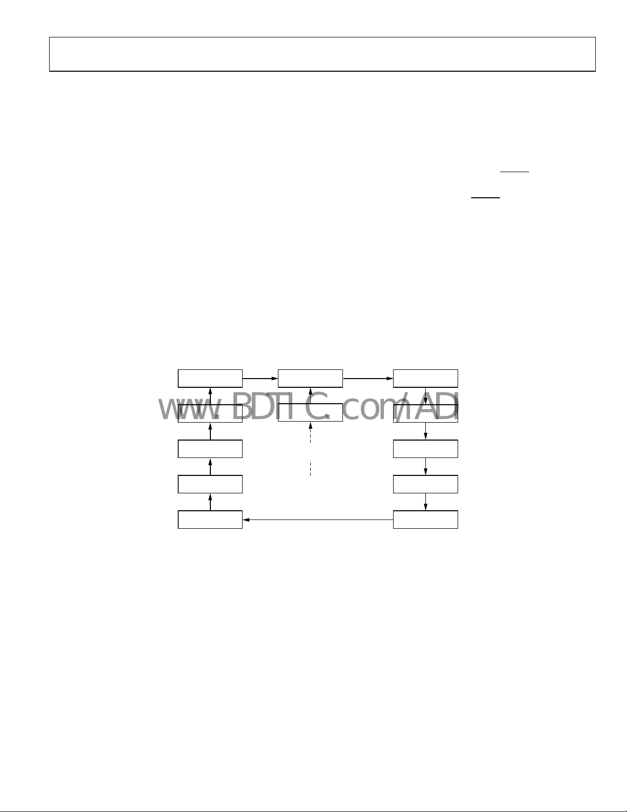
During a power-up sequence, the state machine enables each
power supply in turn. The supply output voltage is monitored to
determine whether it rises above the UV threshold level within
a user defined duration called the blanking time. If a supply
rises above the UV threshold, the next enable output in the
sequence is turned on. In addition to the blanking time, the
user can also define a sequence time delay before each enable
output is turned on.
The ADM1186-1 provides an open-drain pin, SEQ_DONE,
th
at is asserted high to provide an indication that a power-up
sequence is complete. The SEQ_DONE pin allows multiple
cascaded ADM1186-1 devices to perform controlled power-up
and power-down sequences.
During a power-down sequence, the enable outputs turn off
n reverse order. The same sequence time delays used during
i
the power-up sequence are also used during the power-down
sequence as each enable output is turned off; no blanking time
is used during a power-down sequence. At the end of a powerdown sequence, the SEQ_DONE pin is brought low.
POWER-DOWN
DONE
WAIT STAR T
During sequencing and when powered up, the state machine
co
ntinuously monitors the part for any fault conditions. Faults
include a UV condition on any of the inputs or an unexpected
control input. Any fault causes the state machine to enter a fault
handler, which immediately turns off all enable outputs and
then ensures that the device is ready to start a new power-up
sequence.
ULT
FA
The ADM1186-1 has a bidirectional pin,
, that facilitates
fault handling when using multiple devices. If an ADM1186-1
experiences a fault condition, the
FAU LT
pin is driven low,
causing other connected ADM1186-1 devices to enter their own
fault handling states.
The ADM1186-1 is available in a 20-lead QSOP package, and
th
e ADM1186-2 is available in a 16-lead QSOP package.
SEQUENCE UP
TRIGGER
SEQUENCE
SUPPLY 1 ON
SEQUENCE
SUPPLY 1 OFF
SEQUENCE
SUPPLY 2 OFF
SEQUENCE
SUPPLY 3 OFF
SEQUENCE
SUPPLY 4 OFF
FAULT HANDLER
FAULT CONDITION OCCURS
IN ANY STATE
SEQUENCE DOWN TRIGGER
Figure 2. Simplified State Machine Diagram
SEQUENCE
SUPPLY 2 ON
SEQUENCE
SUPPLY 3 ON
SEQUENCE
SUPPLY 4 ON
POWER-UP DONE
07153-004
Rev. 0 | Page 3 of 28
ADM1186
www.BDTIC.com/ADI
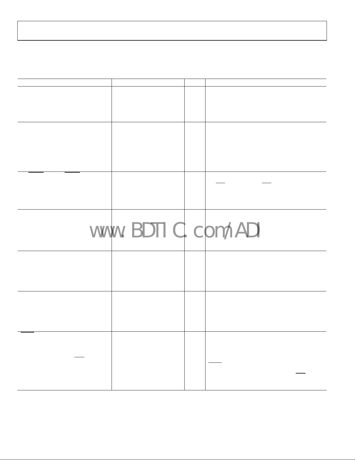
SPECIFICATIONS
V
= 2.7 V to 5.5 V, TA = −40°C to +85°C; typical values at TA = 25°C, unless otherwise noted.
VCC
Table 1.
Parameter Min Typ Max Unit Test Conditions/Comments
VCC PIN
Operating Voltage Range, V
Undervoltage Lockout, V
Undervoltage Lockout Hysteresis 50 mV
Supply Current, I
146 210 µA Steady state; sequence complete
VCC
VIN1 TO VIN4 (VINx) PINS
Input Current −25 +25 nA V
−100 +100 nA V
Input Threshold
1
Input Glitch Immunity
Positive Glitch Duration 19.9 26.6 33.2 µs 50 mV input overdrive
Negative Glitch Duration 2.75 4.7 6.6 µs 50 mV input overdrive
UP, DOWN, AND UP/DOWN PINS
Input Current −100 +100 nA V
Input Threshold
1
Input Glitch Immunity 3.3 6.8 9.7 µs 100 mV input overdrive
2.7 4.9 7.9 µs 1 V input overdrive
DLY_EN_OUTx AND BLANK_DLY PINS
Time Delay Accuracy 5 9 %
Time Delay Charge Current 14 µA
Time Delay Threshold 1.4 V
Time Delay Discharge Resistor 450 Ω
OUT1 TO OUT4 (OUTx) PINS
Output Low Voltage, V
Leakage Current
V
That Guarantees Valid Outputs 1 V
VCC
PWRGD PIN
Output Low Voltage, V
Leakage Current
V
That Guarantees Valid Outputs 1 V
VCC
FAU LT PIN
Input Threshold
1
Input Glitch Immunity 3.1 5.6 8.1 µs 1 V input overdrive
Output Low Voltage, V
Leakage Current
V
That Guarantees Valid Outputs 1 V
VCC
2.7 3.3 5.5 V
VCC
2.46 V V
UVLO
0.5952 0.6000 0.6048 V
1.372 1.4 1.428 V
0.4 V V
OUTL
1 µA OUTx = 5.5 V
0.4 V V
PWRGDL
1 µA PWRGD = 5.5 V
1.372 1.4 1.428 V
0.4 V V
FAULT L
1 µA
falling
VCC
= 0 V to 1 V
VINx
= 0 V to 5.5 V; V
VINx
= 0 V to 5.5 V; V
UP/
DOWN
can be greater than V
VINx
can be greater than V
UP/
DOWN
VCC
VCC
External capacitor values of 10 nF to 2.2 F; excludes
ternal capacitor tolerance
ex
= 2.7 V, I
VCC
Output is guaranteed to be either low (V
or giving a valid output level from V
30 µA or V
= 2.7 V, I
VCC
Output is guaranteed to be either low (V
or giving a valid output level from V
30 µA or V
= 2.7 V, I
VCC
= 5.5 V
FAU LT
Output is guaranteed to be either low (V
or giving a valid output level from V
30 µA or V
SINK
= 1.1 V, I
VCC
SINK
= 1.1 V, I
VCC
SINK
= 1.1 V, I
VCC
= 2 mA
SINK
= 2 mA
SINK
= 2 mA
SINK
= 100 µA
= 100 µA
= 100 µA
VCC
VCC
VCC
OUTL
= 1 V, I
PWRGDL
= 1 V, I
FAULT L
= 1 V, I
= 0.4 V)
=
SINK
= 0.4 V)
=
SINK
= 0.4 V)
=
SINK
Rev. 0 | Page 4 of 28
ADM1186
www.BDTIC.com/ADI
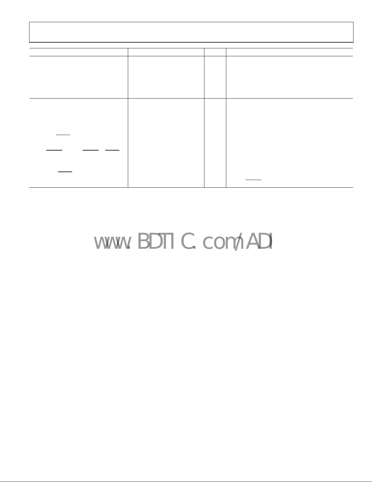
Parameter Min Typ Max Unit Test Conditions/Comments
SEQ_DONE PIN
Output Low Voltage, V
Leakage Current
V
That Guarantees Valid Outputs 1 V
VCC
RESPONSE TIMING
VINx to PWRGD
VINx Going Low to High 21.9 28.8 35.2 µs 50 mV input overdrive
VINx Going High to Low 5.8 7.3 8.9 µs 50 mV input overdrive
VINx to FAULT, OUTx Low
VINx Going High to Low (UV Fault) 6.1 7.5 9.2 µs 50 mV input overdrive
UP, DOWN, and UP/DOWN to FAULT,
OUTx Low, t
UDOUT
5.8 7.7 10.5 µs 1 V input overdrive
External FAULT to OUTx Low
Fault Hold Time 35 44 54 µs
1
Input comparators do not include hysteresis on their inputs. The comparator output passes through a digital glitch filter to remove short transients from the input
signal that would otherwise drive the state machine.
0.4 V V
SEQ_DONEL
1 µA SEQ_DONE = 5.5 V
5.5 8.6 12.1 µs 100 mV input overdrive
10 µs 1 V input overdrive
= 2.7 V, I
VCC
Output is guaranteed to be either low (V
or giving a valid output level from V
or V
= 1.1 V, I
VCC
= 2 mA
SINK
SINK
= 100 µA
VCC
SEQ_DONEL
= 1 V, I
= 0.4 V)
= 30 µA
SINK
Includes input glitch filter and all other internal
ays
del
UP, UP/DOWN
held low
Rev. 0 | Page 5 of 28
ADM1186
www.BDTIC.com/ADI
ABSOLUTE MAXIMUM RATINGS
TA = 25°C, unless otherwise noted.
Table 2.
Parameter Rating
VCC Pin −0.3 V to +6 V
VINx Pins −0.3 V to +6 V
UP, DOWN, UP/DOWN Pins
DLY_EN_OUTx, BLANK_DLY Pins −0.3 V to VCC + 0.3 V
PWRGD, SEQ_DONE, OUTx Pins −0.3 V to +6 V
FAU LT Pin
Operating Temperature Range −40°C to +85°C
Storage Temperature Range −65°C to +150°C
Lead Temperature Convection Reflow
Peak Temperature 260°C
Time at Peak Temperature ≤30 sec
Junction Temperature 125°C
Stresses above those listed under Absolute Maximum Ratings
may cause permanent damage to the device. This is a stress
rating only; functional operation of the device at these or any
other conditions above those indicated in the operational
section of this specification is not implied. Exposure to absolute
maximum rating conditions for extended periods may affect
device reliability.
−0.3 V to +6 V
−0.3 V to +6 V
Table 3. Thermal Resistance
Package Type θJA Unit
16-Lead QSOP 149.97 °C/W
20-Lead QSOP 125.80 °C/W
ESD CAUTION
Rev. 0 | Page 6 of 28
ADM1186
www.BDTIC.com/ADI
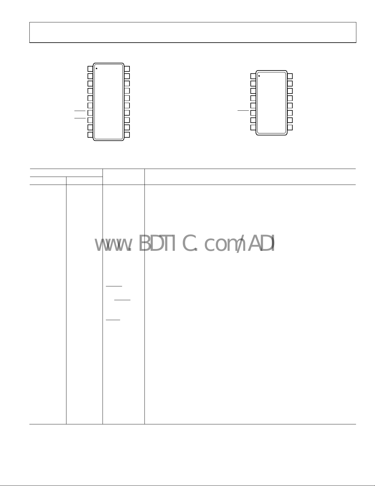
PIN CONFIGURATIONS AND FUNCTION DESCRIPTIONS
GND
VIN1
VIN2
VIN3
VIN4
DOWN
FAULT
DLY_EN_OUT1
DLY_EN_OUT2
UP
1
2
3
ADM1186-1
4
5
(Not to Scale)
6
7
8
9
10
TOP VIEW
20
VCC
19
OUT1
18
OUT2
17
OUT3
16
OUT4
15
PWRGD
14
SEQ_DONE
13
BLANK_DLY
12
DLY_EN_OUT4
11
DLY_EN_OUT3
07153-005
Figure 3. ADM1186-1 Pin Configuration Figure 4. ADM1186-2 Pin Configuration
Table 4. Pin Function Descriptions
Pin No.
ADM1186-1 ADM1186-2
Mnemonic
Description
1 1 GND Chip Ground Pin.
2 2 VIN1
Noninverting Comparator Input. The voltage on this pin is compared with a 0.6 V
reference. Can be used to monitor a voltage rail via a resistor divider. The output of this
comparator is monitored by the state machine.
3 3 VIN2
Noninverting Comparator Input. The voltage on this pin is compared with a 0.6 V
reference. Can be used to monitor a voltage rail via a resistor divider. The output of this
comparator is monitored by the state machine.
4 4 VIN3
Noninverting Comparator Input. The voltage on this pin is compared with a 0.6 V
reference. Can be used to monitor a voltage rail via a resistor divider. The output of this
comparator is monitored by the state machine.
5 5 VIN4
Noninverting Comparator Input. The voltage on this pin is compared with a 0.6 V
reference. Can be used to monitor a voltage rail via a resistor divider. The output of this
comparator is monitored by the state machine.
6 UP
Noninverting Comparator Input. A rising edge on this pin initiates a power-up sequence
when the ADM1186-1 is in the WAIT START state.
7
Noninverting Comparator Input. A falling edge on this pin initiates a power-down
DOWN
sequence when the ADM1186-1 is in the POWER-UP DONE state.
6
UP/DOWN
Noninverting Comparator Input. A rising edge on this pin initiates a power-up sequence
when the ADM1186-2 is in the WAIT START state. A falling edge on this pin initiates a
power-down sequence when the ADM1186-2 is in the POWER-UP DONE state.
8
FAU LT Active Low, Bidirectional, Open-Drain Pin. When an internal fault is detected by the
ADM1186-1 state machine, this pin is asserted low and the SET FAULT state is entered.
An external device pulling this pin low also causes the ADM1186-1 to enter the SET
FAU LT s tate.
9 DLY_EN_OUT1
Timing Input. The capacitor connected to this input sets the time delay between the UP
input initiating a power-up sequence and OUT1 being asserted high. During a powerdown sequence, this input sets the time delay between OUT1 being asserted low and
SEQ_DONE being asserted low.
10 7 DLY_EN_OUT2
Timing Input. The capacitor connected to this input sets the time delay between VIN1
coming into compliance and OUT2 being asserted high during a power-up sequence.
During a power-down sequence, this input sets the time delay between OUT2 being
asserted low and OUT1 being asserted low.
11 8 DLY_EN_OUT3
Timing Input. The capacitor connected to this input sets the tim
coming into compliance and OUT3 being asserted high during a power-up sequence.
During a power-down sequence, this input sets the time delay between OUT3 being
asserted low and OUT2 being asserted low.
1
GND
2
VIN1
ADM1186-2
3
VIN2
VIN3
VIN4
UP/DOWN
DLY_EN_OUT2
DLY_EN_OUT3 DLY_EN_OUT4
TOP VIEW
4
(Not to Scale)
5
6
7
8
16
VCC
15
OUT1
14
OUT2
13
OUT3
12
OUT4
11
PWRGD
10
BLANK_DLY
9
e delay between VIN2
07153-006
Rev. 0 | Page 7 of 28

ADM1186
www.BDTIC.com/ADI
Pin No.
ADM1186-1 ADM1186-2
12 9 DLY_EN_OUT4
13 10 BLANK_DLY
14 SEQ_DONE
15 11 PWRGD
16 12 OUT4
17 13 OUT3
18 14 OUT2
19 15 OUT1
20 16 VCC Positive Supply Input Pin. The operating supply voltage range is 2.7 V to 5.5 V.
Mnemonic Description
Timing Input. The capacitor connected to this input sets the tim
coming into compliance and OUT4 being asserted high during a power-up sequence.
During a power-down sequence, this input sets the time delay between OUT4 being
asserted low and OUT3 being asserted low.
Timing Input. The capacitor connected to this input sets the bla
time allowed between OUTx being asserted and VINx coming into compliance; otherwise,
the SET FAULT state is entered.
Active High, Open-Drain Output. This output is pulled
power-up sequence is complete, SEQ_DONE is asserted high. During a power-down
sequence, the pin remains asserted until the time delay set by DLY_EN_OUT1 has
elapsed. When a fault occurs, this pin is asserted low.
Active High, Open-Drain Output. This output is pulled
state of this pin is a logical AND function of the UV threshold state of the VINx pins. When
the voltage on all VINx inputs exceeds 0.6 V, PWRGD is asserted. This output is driven low
if the voltage on any VINx pin is below 0.6 V.
Active High, Open-Drain Output. This output is pulled
power-up sequence, this output is asserted high after the time delay set by the capacitor
on DLY_EN_OUT4 has elapsed. The output is asserted low immediately after a powerdown sequence has been initiated.
Active High, Open-Drain Output. This output is pulled
power-up sequence, this output is asserted high after the time delay set by the capacitor
on DLY_EN_OUT3 has elapsed. During a power-down sequence, the output is asserted
low after the time delay set by the capacitor on DLY_EN_OUT4 has elapsed.
Active High, Open-Drain Output. This output is pulled
power-up sequence, this output is asserted high after the time delay set by the capacitor
on DLY_EN_OUT2 has elapsed. During a power-down sequence, the output is asserted
low after the time delay set by the capacitor on DLY_EN_OUT3 has elapsed.
Active High, Open-Drain Output. This output is pulled
power-up sequence, this output is asserted high after the time delay set by the capacitor
on DLY_EN_OUT1 has elapsed (ADM1186-1) or immediately after a rising edge on
UP/DOWN (ADM1186-2). During a power-down sequence, the output is asserted low
after the time delay set by the capacitor on DLY_EN_OUT2 has elapsed.
e delay between VIN3
nking time. This is the
low when V
low when V
low when V
low when V
low when V
low when V
= 1 V. When the
CC
= 1 V. The output
CC
= 1 V. During a
CC
= 1 V. During a
CC
= 1 V. During a
CC
= 1 V. During a
CC
Rev. 0 | Page 8 of 28
ADM1186
www.BDTIC.com/ADI
TYPICAL PERFORMANCE CHARACTERISTICS
160
140
120
100
80
60
SUPPLY CURRENT (µA)
40
20
0
0 0.5 1.0 1. 5 2.0 2.5 3.0 3.5 4.0 4.5 5.0 5. 5
SUPPLY VOLTAGE (V)
Figure 5. Supply Current vs. Supply Voltage
150
145
140
135
130
SUPPLY CURRENT (µA)
125
120
–40 –20 0 20 40 60 80
VCC = 5.5V
VCC = 3.3V
VCC = 2.7V
TEMPERATURE (°C)
Figure 6. Supply Current vs. Temperature
605
604
603
602
601
600
599
598
INPUT THRESHOLD (mV)
X
VIN
597
596
595
–40 0 6020–20 40 80
VCC = 3.3V
TEMPERATURE ( °C)
Figure 7. VINx Input Threshold vs. Temperature
07153-007
07153-008
07153-009
38
36
34
32
30
28
26
24
POSITI VE GLI TCH DURATION (µs)
22
20
0 50 100 150 200
VCC = 3.3V
OVERDRIVE (mV)
Figure 8. VINx Input Positive Glitch Immunity vs. Input Overdrive
18
16
14
12
10
8
6
4
NEGATIVE GLITCH DURATION (µs)
2
0
0 50 100 150 200
Figure 9. VINx Input Negative Glitch I
31.0
30.5
30.0
29.5
29.0
28.5
28.0
27.5
27.0
POSITI VE GLI TCH DURATION ( µs)
26.5
26.0
–40 –20 0 20 40 60 80
VCC = 3.3V
OVERDRIVE (mV)
mmunity vs. Input Overdrive
VCC = 3.3V
TEMPERATURE (° C)
Figure 10. VINx Input Positive Glitch Immunity vs. Temperature
07153-010
07153-011
07153-012
Rev. 0 | Page 9 of 28

ADM1186
www.BDTIC.com/ADI
6.0
5.8
5.6
5.4
5.2
5.0
4.8
4.6
4.4
NEGATIVE GLITCH DURAT ION (µs)
4.2
4.0
–40 –20 0 20 40 60 80
Figure 11. VINx Input Negative Gl
1.43
1.42
1.41
1.40
THRESHOLD (V)
1.39
1.38
1.37
–40 0 6020–20 40 80
DOWN
Figure 12. UP,
10.0
9.5
9.0
8.5
8.0
7.5
7.0
6.5
INPUT GL ITCH DURATIO N (µs)
6.0
5.5
5.0
Figure 13. UP,
, UP/
DOWN
VCC = 3.3V
TEMPERATURE ( °C)
itch Immunity vs. Temperature
VCC = 3.3V
TEMPERATURE (° C)
DOWN, FAULT
, and Time Delay Trip Threshold
vs. Temperature
VCC = 3.3V
500 100 150 200
OVERDRIVE (mV)
DOWN
, and UP/
Input Glitch Immunity
vs. Input Overdrive
10.0
9.5
9.0
8.5
8.0
7.5
7.0
6.5
INPUT GLI TCH DURATION (µ s)
6.0
5.5
5.0
–40 –20 0 20 40 60 80
07153-013
DOWN
Figure 14. UP,
10.0
9.5
9.0
8.5
8.0
7.5
7.0
6.5
INPUT GLITCH DURATIO N (µs)
6.0
5.5
5.0
0 200 400 600 800 1000
07153-014
Figure 15.
7.0
6.5
6.0
5.5
INPUT GLITCH DURATIO N (µs)
5.0
–40 0 6020–20 40 80
07153-015
Figure 16.
, and UP/
FAULT
FAULT
VCC = 3.3V
TEMPERATURE ( °C)
DOWN
Input Glitch Immunity vs. Temperature
VCC = 3.3V
OVERDRIVE (mV)
Input Glitch Immunity vs. Input Overdrive
VCC = 3.3V
TEMPERATURE (° C)
Input Glitch Immunity vs. Temperature
07153-016
07153-017
07153-018
Rev. 0 | Page 10 of 28

ADM1186
www.BDTIC.com/ADI
15.0
14.8
14.6
14.4
14.2
14.0
13.8
13.6
CHARGE CURRENT (µA)
13.4
13.2
13.0
VCC = 3.3V
VCC = 2.7V
–40 –20 0 20 40 60
TEMPERATURE (° C)
Figure 17. Time Delay Charge Cu
1k
100
10
TIME DELAY (ms)
VCC = 5.5V
rrent vs. Temperature
07153-019
400
350
300
250
200
150
100
OUTPUT LOW VOLTAGE (mV)
50
1mA
100µA
0
1.0 1.5 2. 0 2.5 3.0 3.5 4.0 4.5 5.0 5.5
SUPPLY VOLTAGE (V)
Figure 20. Output Low Voltage vs. Supply Voltage
9.0
8.5
8.0
7.5
7.0
6.5
RESPONSE TIME (µs)
6.0
07153-022
1
10 100 1k 10k
CAPACITOR (nF )
Figure 18. Time Delay vs. Capacitor Value
600
500
400
300
200
OUTPUT LOW VOLTAGE (mV)
100
0
0 5 10 15 20 25
VCC = 3.3V
OUTPUT SI NK CURRENT (mA)
VCC = 2.7V
V
= 5.5V
CC
Figure 19. Output Low Voltage vs. Output Sink Current
5.5
5.0
2.7 3.2 3.7 4.2 4.7 5.2
07153-020
Figure 21. VINx to
9.0
8.5
8.0
7.5
7.0
6.5
RESPONSE TIME (µs)
6.0
5.5
5.0
–40 –20 0 20 40 60 80
07153-021
Figure 22. VINx to
SUPPLY VOLTAGE (V)
FAULT
, OUTx Low Response Time vs. Supply Voltage
TEMPERATURE (° C)
FAULT
, OUTx Low Response Time vs. Temperature
07153-023
07153-024
Rev. 0 | Page 11 of 28

ADM1186
www.BDTIC.com/ADI
30
25
20
15
RESPONSE T IME (µs)
10
5
0 50 100 150 200
Figure 23. VINx to
VCC = 3.3V
OVERDRIVE (mV)
FAULT
, OUTx Low Response Time vs. Input Overdrive Figure 24. UP,
07153-025
10.0
9.5
9.0
8.5
8.0
7.5
RESPONSE TIME (µs)
7.0
6.5
6.0
2.5 3.0 3.5 4.0 4.5 5.0 5.5
DOWN
SUPPLY VOLTAGE (V)
DOWN
, UP/
to
FAULT
, OUTx Low Response Time
vs. Supply Voltage
07153-026
Rev. 0 | Page 12 of 28

ADM1186
V
V
V
www.BDTIC.com/ADI
THEORY OF OPERATION
The operation of the ADM1186 is described in the following
sections. Where necessary, differences between the ADM1186-1
and the ADM1186-2 are noted.
lock diagram of the ADM1186-1, and Figure 30 is a detailed
b
f
unctional block diagram of the ADM1186-2.
Figure 28 is a detailed functional
The operation of the ADM1186 is described in the context of a
ty
pical voltage monitoring and sequencing application, as shown
in Figure 1. This example uses the ADM1186-1, because it is
es
sentially a superset of the functionality of the ADM1186-2. In
the example application, the ADM1186-1 turns on four regulators,
monitors four separate voltage rails, and generates a power-good
signal to turn on a microcontroller when all power supplies are
on and above their UV threshold level.
M1186-2 voltage sequencing and monitoring application.
AD
Figure 34 shows a typical
UVLO BEHAVIOR
The ADM1186 is designed to ensure that the outputs are always
in a known state for a V
V
supply voltage is below 1 V, the state of the outputs is not
CC
guaranteed. Figure 25 shows the behavior of the outputs over
th
e full V
supply range.
CC
5.5V
2.7V
UVLO
1V
0V
Figure 25. ADM1186 Output Behavior over V
As the VCC supply begins to rise, an undervoltage lockout (UVLO)
circuit becomes active and begins to pull the outputs of the
ADM1186 low. The outputs are not guaranteed to be low until
the V
supply has reached 1 V. State machine operation is also
CC
disabled, so it is not possible to initiate a power-up sequence.
This behavior ensures that enable pins on dc-to-dc converters
o
r point-of-load (POL) devices connected to the OUTx pins are
held low as the supplies are rising. This prevents the dc-to-dc
converters or the POLs from switching on briefly and then
switching off as the supply rails stabilize.
When V
rises above V
CC
the UVLO circuit enables the state machine. The state machine
takes control of the outputs and begins operation from the SET
FAULT state.
supply voltage of 1 V or greater; if the
CC
CC
UNDER STATE
MACHINE CONTRO L
ALL OUT PUTS
UVLO
ACTIVE
and the internal reference is stable,
UVLO
LOW
OUTPUTS
NOT GUARANTEED
07153-027
Supply
CC
After the fault hold time elapses, the state machine moves to the
CLEAR
FAULT state. If the UP (ADM1186-1) or UP/
DOWN
(ADM1186-2) pin is low, the state machine can exit the CLEAR
FAULT state. This change is indicated on the ADM1186-1 by
FAU LT
the
pin being asserted high. For the ADM1186-2, there
is no external indication that the part is ready to perform
sequencing, so 0.5 ms should be allowed after V
comes up
CC
before attempting to start a power-up sequence.
POWER-UP SEQUENCING AND MONITORING
In the example shown in Figure 1, the main supply of 3.3 V
powers up the device via the VCC pin. The state machine remains
in the WAIT START state until either a rising edge on the UP
pin initiates a power-up sequence, or a fault condition occurs.
The ADM1186-2 requires a rising edge on the UP/
to start a power-up sequence.
If a rising edge on the UP pin is detected, the state machine
oves to the DELAY 1 state. The ADM1186-2 does not have a
m
DLY_EN_OUT1 pin, so it omits the DELAY 1 state.
hows the ADM1186-1 state machine in detail; Figure 31 shows
s
th
e ADM1186-2 state machine. The waveforms for a typical
power-up and power-down sequence when no faults occur are
shown in Figure 32 (ADM1186-1) and Figure 33 (ADM1186-2).
In the DELAY 1 state, a time delay, set by the capacitor
co
nnected to the DLY_EN_OUT1 pin, is allowed to elapse.
Then, in the ENABLE OUT1 state, the OUT1 pin is asserted
high. OUT1 is an open-drain, active high output, and in this
application it enables the output of a 2.5 V regulator.
During the ENABLE OUT1 state, the VIN1 pin monitors the
upply after a blanking delay, set by the capacitor on the
2.5 V s
BLANK_DLY pin. The blanking delay, which is the same for all
supplies, is set to allow the slowest rising supply sufficient time
to switch on.
An external resistor divider scales the supply voltage down for
itoring at the VIN1 pin (see Figure 26). The resistor ratio is
mon
s
elected so that the VIN1 voltage is 0.6 V when the supply voltage
rises to the UV level at start-up (a voltage below the nominal 2.5 V
level). In
lev
Figure 26, R1 is 7.4 kΩ and R2 is 2.5 kΩ, so a voltage
el of 2.375 V corresponds to 0.6 V on the noninverting input
of the first comparator.
2.5V
2.375V
t
0V
2.375V SUPPLY
GIVES 0.6V
AT VIN1 PIN
Figure 26. Setting the Undervoltage Threshold
wit
R1
7.4kΩ
VIN1
R2
2.5kΩ
0.6V
h an External Resistor Divider
DOWN
Figure 29
ADM1186
TO LOGIC
CORE
pin
07153-028
Rev. 0 | Page 13 of 28

ADM1186
www.BDTIC.com/ADI
If the output of the 2.5 V regulator meets the UV level when the
blanking time elapses, the state machine continues the power-up
sequence, moving into the DELAY 2 state. A time delay, set by
the capacitor connected to the DLY_EN_OUT2 pin, elapses
before turning on the next enable output, OUT2, in the
ENABLE OUT2 state.
If the 1.8 V supply does not rise to the UV level before the
b
lanking time elapses, sequencing immediately stops and the
state machine enters the SET FAULT state.
The same scheme is implemented with the other output and
nput pins. Every supply turned on via an output pin, OUTx, is
i
monitored via an input pin, VINx, to check that the supply has
risen above the UV level within the blanking time before the
state machine moves on to the next supply.
When a supply is on and operating correctly, the ADM1186
co
ntinues to monitor it for the duration of the power-up
sequence. If any supply drops below its UV threshold level
during a power-up sequence, sequencing stops and the state
machine enters the SET FAULT state.
When the state machine is in the WAIT START state, or at any
ime during a power-up sequence, a falling edge on the
t
pin (ADM1186-1) or the UP/
a fault.
The PWRGD pin is asserted high, independently of the state
achine, when all four VINx pins are above their UV threshold.
m
The state machine in the ADM1186-1 indicates that the powerup sequence is complete by asserting the SEQ_DONE pin high.
DOWN
pin (ADM1186-2) generates
DOWN
OPERATION IN POWER-UP DONE STATE
When the power-up sequence is complete, the state machine
remains in the POWER-UP DONE state until one of the
following events occurs:
• A fal
• A
• A
• An ext
ling edge occurs on the
DOWN
UP/
sequence.
n undervoltage condition occurs on one or more of VIN1
to VIN4, generating a fault.
rising edge occurs on the UP pin, generating a fault
(ADM1186-1 only).
fault (ADM1186-1 only).
(ADM1186-2) pin, initiating a power-down
ernal device brings the
DOWN
(ADM1186-1) or
FAU LT
pin low, causing a
POWER-DOWN SEQUENCING AND MONITORING
When the ADM1186 is in the POWER-UP DONE state, a
falling edge on the
power-down sequence (see Figure 29 or Figure 31).
The state machine moves to the DISABLE OUT4 state, bringing
t
he OUT4 pin low and switching off the 3.3 V regulator. A time
delay, set by the capacitor on the DLY_EN_OUT4 pin, elapses
before the state machine moves to the DISABLE OUT3 state.
DOWN
or UP/
DOWN
pin initiates a
This sequence of steps is repeated until all four regulators
re switched off and the device is in the WAIT START state.
a
Because the ADM1186-2 does not have a DLY_EN_OUT1 pin,
there is no delay between the OUT1 pin being brought low and
the state machine returning to the WAIT START state. When
the device is in the WAIT START state, the SEQ_DONE pin is
brought low.
During a power-down sequence, the state machine monitors the
upplies that are still on. If a supply drops below its UV threshold
s
before it is turned off, the power-down sequence immediately
stops and the state machine enters the SET FAULT state.
DO
WN
A rising edge on the UP or UP/
down sequence generates a fault.
The PWRGD pin is asserted low, independently of the state
achine power-down sequence, when one or more of the
m
VINx pins drops below 0.6 V.
pin during a power-
INPUT GLITCH FILTERING
The VINx, UP,
and the VINx and UP/
time-based glitch filter to prevent false triggering. The glitch
filter avoids the need to use some of the operating supply range
to provide hysteresis on an input. This helps to maximize the
available operating supply range for a system, which is especially
important in systems where low supply voltages are being used.
The VINx inputs use a positive glitch filter that is approximately
ive times longer than the negative glitch filter. This provides
f
additional glitch immunity during the power-up sequence as a
supply is rising, but still allows for a quick response in the event
of an undervoltage event on an input.
DOWN
, and
DOWN
FAU LT
inputs on the ADM1186-1
inputs on the ADM1186-2 use a
FAULT CONDITIONS AND FAULT HANDLING
During supply sequencing and operation in the POWER-UP
DONE state, the ADM1186 continuously monitors the VINx,
DOWN
UP,
FAU LT
faults generated by other devices, which is important during
cascade operation.
The following faults are internally generated:
• A
• A UV condi
• A UV condi
• A fal
• A r
, and UP/
pin on the ADM1186-1 is monitored to detect external
supply fails to reach the UV threshold within the time
defined by the BLANK_DLY capacitor during a power-up
sequence.
has elapsed during a power-up sequence.
disabled during a power-down sequence.
ling edge occurs on the
during a power-up sequence or in the WAIT START state.
ising edge occurs on the UP or UP/
power-down sequence or in the POWER-UP DONE state.
DOWN
pins for fault conditions. The
tion occurs on VINx after the blanking time
tion occurs on VINx before the supply is
or UP/
DOWN
DOWN
pin
pin during a
DOWN
Rev. 0 | Page 14 of 28

ADM1186
www.BDTIC.com/ADI
The action taken by the ADM1186 state machine is the same
for an internal or external fault. The state machine enters the
SET FAULT state, asserts the SEQ_DONE and
(ADM1186-1 only), and asserts all four OUTx enable pins low.
The ADM1186 remains in the SET FAULT state for the fault
old time before moving into the CLEAR FAULT state. If the
h
UP or UP/
state machine enters the CLEAR FAULT state, the state machine
can move immediately into the WAIT ALL OK state.
The length of time from entering the SET FAULT state to
r
eaching the WAIT ALL OK state, with the UP or UP/
pin held low, is the fault hold time. The fault hold time is the
minimum amount of time that the
UP or UP/
the CLEAR FAULT state, the time that the
low is extended.
When the ADM1186-1 is in the CLEAR FAULT state and the
UP p
FAU LT
FAU LT
OK state until the
then transitions into the WAIT START state, ready for the next
power-up sequence.
DOWN
DOWN
in is low, the WAIT ALL OK state is entered and the
pin is deasserted. If an external device is driving the
pin low, the state machine remains in the WAIT ALL
pin is low for a time of t ≥ t
FAU LT
pin is high when the state machine enters
FAU LT
pin returns high. The state machine
FAU LT
pins low
before the
UDOUT
DOWN
pin is held low. If the
FAU LT
pin is held
DEFINING TIME DELAYS
The ADM1186 allows the user to define sequence and blanking
time delays using capacitors. The ADM1186-1 has four
DLY_EN_OUTx pins, and the ADM1186-2 has three
DLY_EN_OUTx pins. Capacitors connected to these pins
control the time delay between supplies turning on or off
during the power-up and power-down sequences. Both devices
provide one pin (BLANK_DLY) to set the blanking time delay.
The ADM1186-1 has a pin called DLY_EN_OUT1 that the
AD
M1186-2 does not have. The capacitor on this pin sets the
time delay used before enabling OUT1 during a power-up
sequence, as well as the time delay between disabling OUT1 and
returning to the WAIT START state during a power-down
sequence. Although this time delay is not essential when a
single ADM1186-1 device is used, the time delay is essential
when multiple devices are cascaded (see the
vices section).
De
When ADM1186-1 devices are used in cascade, the capacitor
o
n the DLY_EN_OUT1 pin of Device N + 1 sets the sequence
time delay between the last supply of Device N and the first
supply of Device N + 1 being turned on and off.
During the power-up sequence, the capacitors connected to the
D
LY_EN_OUTx pins set the time from the end of the blanking
period to the next enable output being asserted high. During
the power-down sequence, the capacitors set the time between
consecutive enable outputs being asserted low.
Cascading Multiple
The blanking time is controlled by the capacitor on the
BL
ANK_DLY pin. This capacitor sets the time allowed between
an enable output being asserted, turning on a supply, and the
output of the supply rising above its defined UV threshold.
A constant current source is connected to a capacitor through a
itch that is under the control of the state machine. This current
sw
source charges a capacitor until the threshold voltage is reached.
For all capacitors, the duration of the time delay is defined by
the following formula:
= C
t
DELAY
where:
t
is the time delay in seconds.
DELAY
is the capacitor value in microfarads (µF).
C
DELAY
For capacitor values from 10 nF to 2.2 F, the time delay is in
th
e range of 1 ms to 220 ms. If a capacitor is not connected to
a timing pin, the time delay is minimal, in the order of several
microseconds.
When a capacitor is not being charged by the current source,
i
t is connected via a resistor to ground. Each capacitor has a
dedicated resistor with a typical value of 450 . To ensure
accurate time delays, time must be allowed for a capacitor to
discharge after it has been used. Typically, allowing five RC time
constants is sufficient for the capacitor to discharge to less than
1% of the threshold voltage.
If the capacitors are not sufficiently discharged after use, the
e delays will be smaller than expected. This can happen if
tim
very small capacitor values are used or if a power-up or powerdown sequence is performed immediately after another
sequence has been completed. Examples of when this behavior
can occur include, but are not limited to, the following:
• A power-down sequence is initiated immediately after
entering the POWER-UP DONE state.
• A fa
• T
To achieve the best timing accuracy over the operational
t
emperature range, the choice of capacitor is critical. Capacitors
are typically specified with a value tolerance of ±5%, ±10%, or
±20%, but in addition to the value tolerance, there is also a
variation in capacitance over temperature.
Where high accuracy timing is important, the use of capacitors
th
capacitance variation of only ±0.3% over the full temperature
range. This capacitance variation contrasts with typical variations of ±15% for X5R and X7R dielectrics and ±22% for X7S
capacitor dielectrics.
ult occurs in the ENABLE OUT1 state when the
DLY_EN_OUT1 capacitor is charged and a power-up
sequence is started very quickly after the fault has been
handled.
he DLY_EN_OUTx time delay is very short and is insuffi-
cient to allow the BLANK_DLY capacitor to fully discharge.
at use a C0G, sometimes called NPO, dielectric results in a
DELAY
× 0.1
Rev. 0 | Page 15 of 28

ADM1186
www.BDTIC.com/ADI
SEQUENCE CONTROL USING A SUPPLY RAIL
DO
The UP and
DOWN
UP/
power-up and power-down sequences. These inputs are
designed for use with digital or analog signals, such as power
supply rails. Using a power supply rail to control the up and
down sequencing allows the ADM1186 to perform sequencing
and monitoring functions for five supply rails.
When using a supply rail to control an ADM1186-1 (with
he UP and
t
some hysteresis is required. The hysteresis is added on the
joined UP and
DOWN
UP/
ramping supply rail does not cause spurious rising or falling
edges that would otherwise cause state machine faults.
To provide the necessary hysteresis, a single additional resistor
(RH in Figure 27) is connected between the joined UP and
DOWN
pins of the ADM1186-1 and the OUT1 pin of the
device, or between the UP/
the OUT1 pin of the device.
VIN
R1
R2
Figure 27. Using a Supply Rail to Control Sequencing with Hysteresis
When OUT1 is low, the resistor RH sinks current from the
node at the midpoint of R1 and R2, slightly increasing the VIN
voltage needed to start a power-up sequence, referred to as V
When OUT1 is high, RH sources current into the midpoint of
R1 and R2, decreasing the VIN voltage necessary to start a
power-down sequence, referred to as V
The hysteresis at the VIN node is simply V
and R2 resistors scale VIN down, the hysteresis on VIN is also
scaled down. The scaled hysteresis, V
UP and
DOWN
(ADM1186-2) must be at least 75 mV. The value of RH is
selected to ensure that this is the case.
H
L
WN
inputs on the ADM1186-1 and the
input on the ADM1186-2 are used to initiate
DOWN
pins connected) or an ADM1186-2,
DOWN
pins of the ADM1186-1 or on the
pin of the ADM1186-2 to ensure that a slowly
DOWN
ADM1186-1
1.4V
+
–
+
–
UP
DOWN
pins (ADM1186-1) or the UP/
⎡
⎛
×+×=
R1V
14.1
⎜
⎢
⎝
⎣
⎡
⎛
⎜
4.1
R1V
⎢
⎜
R2
⎢
⎝
⎣
pin of the ADM1186-2 and
RH
3.3V
VCC
OUT1
STATE
MACHINE
.
L
− VL. As the R1
H
, at the inputs to the
SHYS
+
RH R2
⎤
⎞
⎟
⎥
×
RH R2
⎠
⎦
⎤
⎞
−
VP
4.14.1
−×+=
⎟
⎥
⎟
+
RP RH
⎥
⎠
⎦
DOWN
pin
VP
RP
H
V V V
()
SHYS
LH
In the example application shown in Figure 27, the following
ues could be used:
val
RP = 10 k
VP = 5 V
VIN = 3.3 V
The values of the R1 and R2 resistors determine the midpoint
f the hysteresis, V
o
MID
which power-up and power-down sequences are initiated. For a
3.3 V supply, a threshold just below 3 V could be used, making
R1 = 11 k and R2 = 10 k and giving a midpoint of 2.94 V.
2×
MID
V
MID
=
V
= 2.94 V
RVIN
+
R2R1
As a general rule, the value for RH is approximately 60 times
t
he value of R1 in parallel with R2. In this example, R1 in
parallel with R2 is 5.24 k, so RH would be approximately
314 k. Taking a value of 300 k for RH and using this value
in the previous equations for V
values are obtained:
⎡
⎛
H
V
= 2.991 V
H
⎜
⎢
⎝
⎣
⎡
k114.1
L
= 2.812 V
07153-038
.
V
L
V
SHYS
V
SHYS
⎢
⎢
⎣
()
= 0.085 V
Because the value of V
hysteresis required, the RH resistor value selected is sufficient.
If the value of V
obtained is too small, the value of RH can
SHYS
be reduced, increasing the scaled hysteresis provided.
It should be noted that it is not possible to directly connect the
supply to the UP pin (ADM1186-1) or to the UP/
V
CC
pin (ADM1186-2) to start a sequence as the V
When the UVLO circuit enables the state machine, it begins
in the fault handler states. To reach the WAIT START state so
that sequencing can begin, the UP pin (ADM1186-1) or the
DOWN
UP/
pin (ADM1186-2) must be held low after the state
machine is enabled.
R2
⎛
×−=
⎜
⎝
⎞
⎟
+
R2 R1
⎠
, about which VH and VL set the levels at
k10×3.3
=
×+×=
k1114.1
V
⎛
4.1
⎜
V
⎜
k10
⎝
812.2991.2
is greater than the 75 mV of scaled
SHYS
k10+k11
, VL, and V
H
+
×
−×+=
⎛
×−=
⎜
⎝
, the following
SHYS
⎤
k300 k 10
⎞
⎟
⎥
k300k10
⎠
⎦
⎤
⎞
−
4.15
⎟
⎥
⎟
+
k10k300
⎥
⎠
⎦
k10
⎞
⎟
+
k10k11
⎠
DOWN
comes up.
CC
Rev. 0 | Page 16 of 28

ADM1186
VCC
www.BDTIC.com/ADI
VIN1
VIN2
VIN3
VIN4
UP
DOWN
FAULT
DLY_EN_OUT1
DLY_EN_OUT2
DLY_EN_OUT3
DLY_EN_OUT4
BLANK_DLY
0.6V
1.4V
14µA
450Ω
GLITCH F ILTER
GLITCH F ILTER
GLITCH F ILTER
GLITCH F ILTER
GLITCH F ILTER
GLITCH F ILTER
GLITCH F ILTER
CAPACITOR MUX
AND DISCHARGE
RISING EDGE
DETECT
FALL IN G E DG E
DETECT
1.4V
ADM1186-1
STATE
MACHINE
PWRGD
OUT1
OUT2
OUT3
OUT4
SEQ_DONE
GND
Figure 28. Functional Block Diagram of the ADM1186-1
07153-029
Rev. 0 | Page 17 of 28

ADM1186
www.BDTIC.com/ADI
F
F
FAULT IN: LOW
UP: RISING E DGE
FAULT IN: LOW
UP: RISING E DGE
VIN1: LOW
AFTER DLY_EN_OUT1
TIME DELAY
DISABLE OUT1
OUT1: LOW
AFTER DLY_EN_OUT2
TIME DELAY
DISABLE OUT2
OUT2: LOW
WAI T S TAR T
OUT1: LOW OUT4: LOW
OUT2: LOW SEQ_DONE: LOW
OUT3: LOW FAULT OUT: HIGH
UP: RISING E DGE
FAU LT I N: LO W
DELAY 1
ENABLE OUT1
OUT1: HIGH
DELAY 2
ENABLE OUT2
OUT2: HIGH
DOWN: FALLING EDGE
AFTER DLY_EN_OUT1 TIME DELAY
FAU LT I N: LO W
DOWN: FALLING EDGE
AFTER BLANKING DELAY VIN1: LOW
AFTER BLANKING DELAY VIN1: HIGH
FAU LT I N: LO W
DOWN: FALLING EDGE
VIN1: LOW
AFTER DLY_EN_OUT2 TIME DELAY
FAU LT I N: LO W
DOWN: FALLING EDGE
VIN1: LOW
AFTER BLANKING DELAY VIN2: LOW
AFTER BLANKING DELAY VIN2: HIGH
FAULT IN: HIGH
FAULT IN: LOW
DOWN: FALLING EDGE
WAI T ALL OK
FAULT OUT: HIGH
F
F
F
F
F
UP: LOW
CLEAR FAULT
FAULT HOLD
TIMES OUT
SET FAULT
OUT1: LOW OUT4: LOW
OUT2: LOW SEQ_DONE: LOW
OUT3: LOW FAULT OUT: LOW
F
EXIT UVLO
FAULT IN: LOW
UP: RISING E DGE
VIN1 OR VIN2: LOW
F
FAULT IN: LOW
UP: RISING E DGE
VIN1 OR VIN2 OR VIN3: LOW
F
AFTER DLY_EN_OUT3
TIME DELAY
DISABLE OUT3
OUT3: LOW
AFTER DLY_EN_OUT4
TIME DELAY
DISABLE OUT4
OUT4: LOW
DOWN: FALLING EDGE
FAU LT I N: LO W
DOWN: FALLING EDGE
DELAY 3
ENABLE OUT3
OUT3: HIGH
DELAY 4
ENABLE OUT4
OUT4: HIGH
POWER-UP DONE
SEQ_DONE: HIGH
VIN1 OR VIN2: LOW
AFTER DLY_EN_OUT3 TIME DELAY
FAU LT I N: LO W
DOWN: FALLING EDGE
VIN1 OR VIN2: LOW
AFTER BLANKING DELAY VIN3: LOW
AFTER BLANKING DELAY VIN3: HIGH
FAU LT I N: LO W
DOWN: FALLING EDGE
VIN1 OR VIN2 OR VIN3: LOW
AFTER DLY_EN_OUT4 TIME DELAY
FAU LT I N: LO W
DOWN: FALLING EDGE
VIN1 OR VIN2 OR VIN3: LOW
AFTER BLANKING DELAY VIN4: LOW
AFTER BLANKING DELAY VIN4: HIGH
FAU LT I N: LO W
UP: RISING EDGE
VIN1 OR VIN2 OR VIN3 OR VIN4: LOW
Figure 29. ADM1186-1 State Machine Operation
F
F
F
F
F
07153-030
Rev. 0 | Page 18 of 28

ADM1186
VCC
www.BDTIC.com/ADI
VIN1
VIN2
VIN3
VIN4
UP/DOWN
DLY_EN_OUT2
DLY_EN_OUT3
DLY_EN_OUT4
BLANK_DLY
GLITCH F ILTER
GLITCH F ILTER
GLITCH F ILTER
GLITCH F ILTER
0.6V
1.4V
14µA
450Ω
GLITCH FILTER
CAPACITOR MUX
AND DISCHARGE
GND
EDGE
DETECT
1.4V
STATE
MACHINE
Figure 30. Functional Block Diagram of the ADM1186-2
ADM1186-2
PWRGD
OUT1
OUT2
OUT3
OUT4
07153-031
Rev. 0 | Page 19 of 28

ADM1186
W
www.BDTIC.com/ADI
WAIT START
OUT1: LOW OUT3: LOW
OUT2: LOW OUT4: LOW
UP/DOWN: LO
CLEAR FAULT
FAULT HO LD
TIMES OUT
SET FAULT
F
EXIT UVLO
UP/DOWN: RIS ING EDGE
F
UP/DOWN: RIS ING EDGE
VIN1: LOW
F
UP/DOWN: RIS ING EDGE
VIN1 OR VIN2: L OW
F
DISABLE OUT1
OUT1: LOW
AFTER DLY_EN_OUT2
TIME DELAY
DISABLE OUT2
OUT2: LOW
AFTER DLY_EN_OUT3
TIME DELAY
DISABLE OUT3
OUT3: LOW
UP/DOWN: RI SING EDGE
UP/DOWN: FALLING EDGE
ENABLE OUT1
OUT1: HIGH
DELAY 2
ENABLE OUT2
OUT2: HIGH
DELAY 3
ENABLE OUT3
OUT3: HIGH
AFTER BLANKI NG DELAY VIN1: LOW
AFTER BLANKING DELAY VIN1: HIGH
UP/DOWN: FALLING EDGE
VIN1: LOW
AFTER DLY_EN_OUT2 TIME DELAY
UP/DOWN: FALLING EDGE
VIN1: LOW
AFTER BLANKI NG DELAY VIN2: LOW
AFTER BLANKING DELAY VIN2: HIGH
UP/DOWN: FALLING EDGE
VIN1 OR VIN2: LOW
AFTER DLY_EN_OUT3 TIME DELAY
UP/DOWN: FALLING EDGE
VIN1 OR VIN2: LOW
AFTER BLANKI NG DELAY VIN3: LOW
AFTER BLANKING DELAY VIN3: HIGH
F
OUT1: LOW OUT3: LOW
OUT2: LOW OUT4: LOW
F
F
F
F
UP/DOWN: RIS ING EDGE
VIN1 OR VIN2 OR VIN3: L OW
F
AFTER DLY_EN_OUT4
TIME DELAY
DISABLE OUT4
OUT4: LOW
UP/DOWN: FALLING EDGE
UP/DOWN: FALLING EDGE
DELAY 4
ENABLE OUT4
OUT4: HIGH
POWER-UP DONE
VIN1 OR VIN2 OR VIN3: LOW
AFTER DLY_EN_OUT4 TIME DELAY
UP/DOWN: FALLING EDGE
VIN1 OR VIN2 OR VIN3: LOW
AFTER BLANKI NG DELAY VIN4: LOW
AFTER BLANKING DELAY VIN4: HIGH
VIN1 OR VIN2 OR VIN3 OR VIN4: LOW
Figure 31. ADM1186-2 State Machine Operation
F
F
F
07153-032
Rev. 0 | Page 20 of 28

ADM1186
www.BDTIC.com/ADI
12 34 6 7 10 1211895 13 14 1
UP
DOWN
DLY_EN_OUT1
OUT1
DLY_EN_OUT2
OUT2
DLY_EN_OUT3
OUT3
DLY_EN_OUT4
OUT4
BLANK_DLY
SEQ_DONE
PWRGD
STATE NAMES
1 - WAIT START
2 - DELAY 1
3 - ENABLE OUT1
4 - DELAY 2
5 - ENABLE OUT 2
6 - DELAY 3
7 - ENABLE OUT3
8 - DELAY 4
9 - ENABLE OUT4
10 - POWER-UP DONE
11 - DISABLE OUT4
12 - DISABLE O UT3
13 - DISABLE O UT2
14 - DISABLE O UT1
07153-033
Figure 32. ADM1186-1 Typical Power-Up and Power-Down Sequence Waveforms with Corresponding State Names
12 3 4 5 678 9 10 11 1213 1
UP/DOWN
OUT1
DLY_EN_OUT2
OUT2
DLY_EN_OUT3
OUT3
DLY_EN_OUT4
OUT4
BLANK_DLY
PWRGD
1 - WAIT START
2 - ENABLE OUT1
3 - DELAY 2
4 - ENABLE OUT 2
5 - DELAY 3
6 - ENABLE OUT 3
STATE NAMES
7 - DELAY 4
8 - ENABLE OUT4
9 - POWER-UP DONE
Figure 33. ADM1186-2 Typical Power-Up and Power-Down Sequence Waveforms with Corresponding State Names
Rev. 0 | Page 21 of 28
10 - DISABLE O UT4
11 - DISABLE OUT3
12 - DISABLE O UT2
13 - DISABLE O UT1
07153-037

ADM1186
V
www.BDTIC.com/ADI
5V
3.3V AUX
1µF
100nF
VCC OUT1 OUT2
SEQUENCE CONT ROL
UP/DOWN
ADM1186-2
DLY_EN_OUT2
DLY_EN_OUT3
DLY_EN_OUT4
BLANK_DLY
ADP1706
EN OUT
5V
GND
5
IN
ADP2107
EN OUT
3.3V AUX
OUT3 OUT4
PWRGD
5V
IN
5V
VIN1
VIN2
VIN3
VIN4
3.3V AUX
IN
ADP1821
EN OUT
2.5V AUX
5V
IN
ADP1706
EN OUT
2.5V
1.8V
1.2V
3.3V
07153-034
Figure 34. ADM1186-2 Typical Application
Rev. 0 | Page 22 of 28

ADM1186
www.BDTIC.com/ADI
CASCADING MULTIPLE DEVICES
Multiple ADM1186-1 devices can be cascaded in applications
that require more than four supplies to be sequenced and
monitored. When ADM1186-1 devices are cascaded, the
controlled power-up and power-down of all the cascaded
supplies is maintained using only three pins on each device.
There are several configurations for interconnecting these
de
vices. The most suitable configuration depends on the
application. Figure 35 and Figure 36 show two methods for
cading multiple ADM1186-1 devices.
cas
Figure 35 shows a single sequence of 12 supplies. The capacitors
us
ed for timing are not shown in the figure for clarity. To ensure
controlled power-up and power-down sequencing of all 12 supplies, the following connections are made:
•
The UP pin of the first device and the
last device in the cascade chain are connected.
•
The SEQ_DONE pin of Device N is connected to the UP
pin of Device N + 1.
•
The SEQ_DONE pin of Device N is connected to the
DOWN
pin of Device N − 1.
When the SEQUENCE CONTROL line goes high, Device A
gins the power-up sequence, turning on each enable output
be
in turn, with the associated delays, according to the state
machine. When Device A completes its power-up sequence, the
SEQ_DONE pin goes from low to high, initiating a power-up
sequence on Device B. When Device B completes its power-up
sequence, the Device B SEQ_DONE pin goes high, initiating a
power-up sequence on Device C. When Device C completes its
power-up sequence and all supplies are above the UV threshold,
the system POWER GOOD signal goes high.
If the SEQUENCE CONTROL line goes low, Device C starts a
ower-down sequence, turning off its enable outputs. When all
p
Device C enable outputs are off, the SEQ_DONE pin on Device C
goes low, causing a high-to-low transition on the
Device B. This transition initiates a power-down sequence on
Device B, which takes all its OUTx pins low, causing SEQ_DONE
to be taken low. This high-to-low transition is seen by Device A,
which starts its power-down sequence, thus completing the
ordered shutdown of the 12 supplies.
Note that the capacitor on the DLY_EN_OUT1 pin of Device B
(n
ot shown in Figure 35) sets the sequence time delay between
e last supply of Device A and the first supply of Device B
th
being turned on and off.
DOWN
pin of the
DOWN
pin of
Figure 36 shows two independent sequences of four supplies,
ch with common status outputs. In this example, both devices
ea
share the same sequence control signal, so they start their
power-up and power-down sequences at the same time. Both
devices must complete their power-up sequences before the
POWER GOOD signal goes high.
FA
ULT
The
Connecting the
on one device, or an unexpected event such as a rising or falling
edge on the UP or
all the other devices.
When an internal fault condition occurs on a device, it pulls its
FAU LT
devices to enter the SET FAULT state and pull their
low. Each device waits for the fault hold time to elapse and then
moves to the CLEAR FAULT state.
If the V
UVLO circuit becomes active, and the
This generates a fault condition on all other connected devices.
A device in the CLEAR FAULT state holds its
until its UP input pin is low. The device then moves into the
WAIT ALL OK state and releases the
If, for example, a UV fault occurs on a VINx pin during a
ower-up sequence, the UP pin will be high on the first device
p
in the cascade. The first device in the cascade holds the
line low until the UP pin is brought low. All other devices will
have released their
OK state.
When the UP pin goes low, the first device releases its
pin so the
move together from the WAIT ALL OK state back into the
WAIT START state, ready for the next power-up sequence.
An external device such as a microcontroller, field programmable
ga
te array (FPGA), or an overtemperature sensor can cause a
fault condition by briefly bringing
ADM1186-1 behaves as described. If the external device continues
to hold the
in the WAIT ALL OK state, effectively preventing a power-up
sequence from starting.
pins of all devices in a cascade should be connected.
FAU LT
pins ensures that an undervoltage fault
DOWN
pin low. This in turns causes the other ADM1186-1
supply for an ADM1186-1 drops below V
CC
FAU LT
line returns high, which allows all devices to
FAU LT
line low, all the ADM1186-1 devices remain
pin, generates a fault condition on
FAU LT
FAU LT
FAU LT
pins and will be in the WAIT ALL
FAU LT
low. In this case, the
FAU LT
, the
UVLO
pin is pulled low.
FA
ULT
pin low
pin.
FAU LT
FA
ULT
pins
Rev. 0 | Page 23 of 28

ADM1186
V
V
www.BDTIC.com/ADI
POWER
GOOD
3.3
ENABLE
OUTPUTS TO
REGULATORS
WITH PULL-UPs
AS REQUIRED
EN9
EN10
EN11
EN12
OUT1
OUT2
OUT3
OUT4
FAULT
PWRGD
VCC
VIN1
VIN2
VIN3
VIN4
ADM1186-1C
V9
V10
V11
UP
V12
3.3V
GND
SEQ_DONE
DOWN
3.3V
07153-035
EN5
EN6
EN7
EN8
OUT1
OUT2
OUT3
OUT4
FAULT
VCC
VIN1
VIN2
VIN3
EN2
EN3
OUT2
OUT3
VIN2
VIN3
V2V3V4
VIN4
V8
3.3V
VIN4
ADM1186-1B
V5V6V7
EN1
OUT1
VCC
VIN1
ADM1186-1A
3.3
V1
PWRGD
GND
SEQ_DONE
UP
DOWN
EN4
OUT4
FAULT
PWRGD
GND
SEQ_DO NE
UP
DOWN
DIVIDERS
SUPPLIES
ITH RESISTOR
SCALED DOWN
Figure 35. Cascading Multiple ADM1186-1 Devices, Option 1
Rev. 0 | Page 24 of 28
SEQUENCE CONT ROL

ADM1186
V
www.BDTIC.com/ADI
3.3
VCC
ADM1186-1A
SEQUENCE CONTRO L
SUPPLIES
SCALED
DOWN WITH
RESISTOR
DIVIDERS
V1
V2
V3
V4
VIN1
VIN2
VIN3
VIN4
UP
DOWN
OUT1
OUT2
OUT3
OUT4
FAULT
PWRGD
SEQ_DONE
GND
3.3V
VCC
EN1
ENABLE
EN2
OUTPUTS TO
REGULATORS
WITH PULL-UPs
EN3
AS REQUIRED
EN4
NO CONNECT
3.3V
ADM1186-1B
V5
V6
V7
V8
VIN1
VIN2
VIN3
VIN4
UP
DOWN
OUT1
OUT2
OUT3
OUT4
FAULT
PWRGD
SEQ_DONE
GND
EN5
EN6
EN7
EN8
NO CONNECT
5V
POWER
GOOD
07153-036
Figure 36. Cascading Multiple ADM1186-1 Devices, Option 2
Rev. 0 | Page 25 of 28

ADM1186
www.BDTIC.com/ADI
OUTLINE DIMENSIONS
0.345 (8.76)
0.341 (8.66)
0.337 (8.55)
0.065 (1.65)
0.049 (1.25)
0.010 (0.25)
0.004 (0.10)
COPLANARITY
0.004 (0.10)
20
1
0.025 (0.64)
BSC
CONTROLL ING DIMENSIONS ARE IN INCHES; MILLIMETERS DIMENSIO NS
(IN PARENTHESES) ARE ROUNDED-O FF INCH EQ UIVALENTS FOR
REFERENCE ON LY AND ARE NOT APPROPRI ATE FOR USE IN DESIGN.
0.012 (0.30)
0.008 (0.20)
COMPLIANT TO JEDEC STANDARDS MO-137-AD
11
10
0.158 (4.01)
0.154 (3.91)
0.150 (3.81)
0.069 (1.75)
0.053 (1.35)
SEATING
PLANE
0.244 (6.20)
0.236 (5.99)
0.228 (5.79)
8°
0°
0.010 (0.25)
0.006 (0.15)
0.050 (1.27)
0.016 (0.41)
0.020 (0.51)
0.010 (0.25)
0.041 (1.04)
REF
012808-A
Figure 37. 20-Lead Shrink Small Outline Package [QSOP] (RQ-20)
Dim
ensions shown in inches and (millimeters)
0.197 (5.00)
0.193 (4.90)
0.189 (4.80)
16
1
9
8
0.158 (4.01)
0.154 (3.91)
0.150 (3.81)
0.244 (6.20)
0.236 (5.99)
0.228 (5.79)
0.065 (1.65)
0.049 (1.25)
0.010 (0.25)
0.004 (0.10)
COPLANARIT Y
0.004 (0.10)
8°
0°
0.010 (0.25)
0.006 (0.15)
0.050 (1.27)
0.016 (0.41)
0.069 (1.75)
0.053 (1.35)
SEATING
0.025 (0.64)
BSC
CONTROLL ING DIMENSIONS ARE IN INCHES; MIL LIMETERS DIMENSIO NS
(IN PARENTHESES) ARE ROUNDED-O FF INCH EQ UIVALENTS FOR
REFERENCE ON LY AND ARE NOT APPROPRI ATE FOR USE IN DESIGN.
0.012 (0.30)
0.008 (0.20)
COMPLIANT TO JEDEC STANDARDS MO-137-AB
PLANE
0.020 (0.51)
0.010 (0.25)
0.041 (1.04)
REF
012808-A
Figure 38. 16-Lead Shrink Small Outline Package [QSOP] (RQ-16)
ensions shown in inches and (millimeters)
Dim
ORDERING GUIDE
Model Temperature Range Package Description Package Option
ADM1186-1ARQZ
ADM1186-1ARQZ-REEL
ADM1186-2ARQZ
ADM1186-2ARQZ-REEL
EVAL-ADM1186-1EBZ
EVAL-ADM1186-1MBZ
EVAL-ADM1186-2EBZ
EVAL-ADM1186-2MBZ
1
Z = RoHS Compliant Part.
1
1
1
1
1
1
1
1
−40°C to +85°C 20-Lead Shrink Small Outline Package [QSOP] RQ-20
−40°C to +85°C 20-Lead Shrink Small Outline Package [QSOP] RQ-20
−40°C to +85°C 16-Lead Shrink Small Outline Package [QSOP] RQ-16
−40°C to +85°C 16-Lead Shrink Small Outline Package [QSOP] RQ-16
Evaluation Kit
Micro-Evaluation Kit
Evaluation Kit
Micro-Evaluation Kit
Rev. 0 | Page 26 of 28

ADM1186
www.BDTIC.com/ADI
NOTES
Rev. 0 | Page 27 of 28

ADM1186
www.BDTIC.com/ADI
NOTES
©2008 Analog Devices, Inc. All rights reserved. Trademarks and
registered trademarks are the property of their respective owners.
D07153-0-5/08(0)
Rev. 0 | Page 28 of 28
 Loading...