

VCC
0.8% Accurate Quad Voltage Monitor
FEATURES
Powered from 2.7 V to 5.5 V on the VCC pin
Monitors 4 supplies via 0.8% accurate comparators
4 inputs can be programmed to monitor different voltage
levels with external resistor dividers
3 open-drain enable outputs (OUT1, OUT2, and OUT3)
Open-drain power-good output (PWRGD)
Internal 190 ms delay associated with assertion of PWRGD
10-lead MSOP
APPLICATIONS
Monitor and alarm functions
Telecommunications
Microprocessor systems
PC/servers
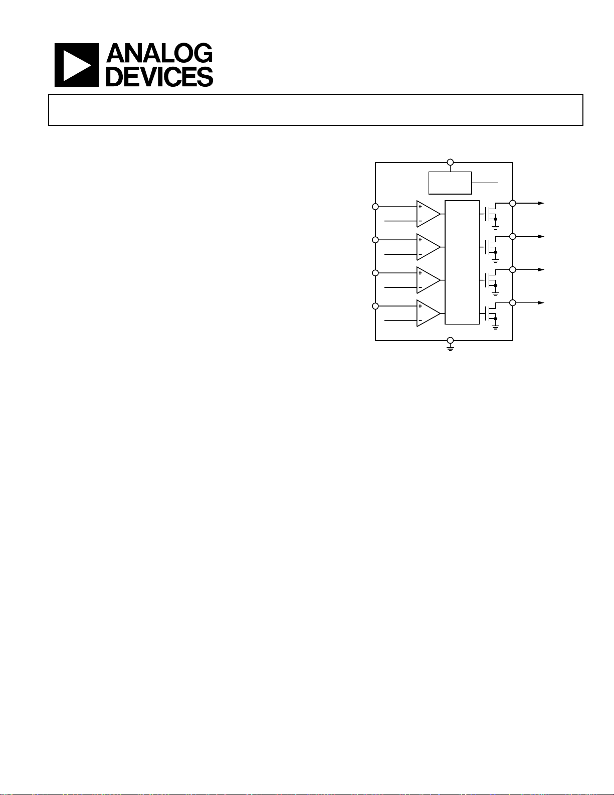
GENERAL DESCRIPTION
The ADM1184 is an integrated, 4-channel voltage-monitoring
device. A 2.7 V to 5.5 V power supply is required on the VCC pin
to power the device.
Four precision comparators monitor four voltage rails.
Each comparator has a 0.6 V reference with a worst-case
accuracy of 0.8%. Resistor networks that are external to the
VIN1, VIN2, VIN3, and VIN4 pins set the trip points for
the monitored supply rails.
The ADM1184 has four open-drain outputs. OUT1 to OUT3
can be used to enable power supplies, and PWRGD is a
common power-good output.
ADM1184
FUNCTIONAL BLOCK DIAGRAM
POWER AND
ADM1184
VIN1
REF = 0.6V
VIN2
REF = 0.6V
VIN3
REF = 0.6V
VIN4
REF = 0.6V
REFERENCE
GENERATOR
GND
Figure 1.
OUT1 to OUT3 are dependent on their associated VINx input
(that is, VIN1, VIN2, or VIN3). If a supply monitored by VINx
drops below its programmed threshold, the associated OUTx pin
and PWRGD are disabled.
PWRGD is a common power-good output indicating the status
of all monitored supplies. There is an internal 190 ms (typical)
delay associated with the assertion of the PWRGD output. If
VIN1, VIN2, VIN3, or VIN4 drops below its programmed
threshold, PWRGD is deasserted immediately.
The ADM1184 is available in a 10-lead mini small outline
package (MSOP).
INTERNAL
LOGIC
REF = 0.6V
OUT1
OUT2
OUT3
PWRGD
07352-001
Rev. 0
Information furnished by Analog Devices is believed to be accurate and reliable. However, no
responsibility is assumed by Anal og Devices for its use, nor for any infringements of patents or ot her
rights of third parties that may result from its use. Specifications subject to change without notice. No
license is granted by implication or otherwise under any patent or patent rights of Analog Devices.
Trademarks and registered trademarks are the property of their respective owners.
One Technology Way, P.O. Box 9106, Norwood, MA 02062-9106, U.S.A.
Tel: 781.329.4700 www.analog.com
Fax: 781.461.3113 ©2008 Analog Devices, Inc. All rights reserved.

ADM1184
TABLE OF CONTENTS
Features .............................................................................................. 1
Applications....................................................................................... 1
Functional Block Diagram .............................................................. 1
General Description......................................................................... 1
Revision History ............................................................................... 2
Specifications..................................................................................... 3
Absolute Maximum Ratings............................................................ 4
Thermal Resistance ...................................................................... 4
ESD Caution.................................................................................. 4
REVISION HISTORY
2/08—Revision 0: Initial Version
Pin Configuration and Function Descriptions..............................5
Typical Perf or m an c e Charac t e r istics ..............................................6
Theory of Operation .........................................................................9
Input Configuration......................................................................9
Output Configuration...................................................................9
Voltage Monitoring and Sequencing Application.................. 11
Outline Dimensions ....................................................................... 12
Ordering Guide .......................................................................... 12
Rev. 0 | Page 2 of 12

ADM1184
SPECIFICATIONS
VCC = 2.7 V to 5.5 V, TA = −40°C to +85°C.
Table 1.
Parameter Min Typ Max Unit Conditions
VCC Pin
Operating Voltage Range, V
Supply Current, I
VCC
CC
VIN1 to VIN4 (VINx) Pins
Input Current, I
Input Threshold, V
VINLEAK
TH
OUT1 to OUT3 (OUTx), PWRGD Pins
Output Low Voltage, V
OUTL
0.4 V VCC = 1 V, I
Leakage Current, I
ALERT
VCC that Guarantees Valid Outputs 1 V
TIMING DELAYS Refer to the timing diagrams in Figure 18 and Figure 19
VIN1 to OUT1, VIN2 to OUT2, VIN3 to OUT3
Low-to-High Propagation Delay 30 μs VCC = 3.3 V
High-to-Low Propagation Delay, All Inputs 30 μs VCC = 3.3 V
All Inputs High to PWRGD Rising Delay 100 190 280 ms VCC = 3.3 V
2.7 3.3 5.5 V
24 80 μA
−20 +20 nA V
VINx
= 0.7 V
0.5952 0.6000 0.6048 V
0.4 V VCC = 2.7 V, I
−1 +1 μA
All outputs are guaranteed to be either low or to give
a valid output level from V
= 2 mA
SINK
= 100 μA
SINK
= 1 V
CC
Rev. 0 | Page 3 of 12
ADM1184
ABSOLUTE MAXIMUM RATINGS
TA = 25°C, unless otherwise noted.
Table 2.
Parameter Rating
VCC Pin −0.3 V to +6 V
VINx Pins −0.3 V to +6 V
OUTx, PWRGD Pins −0.3 V to +6 V
Storage Temperature Range −65°C to +125°C
Operating Temperature Range −40°C to +85°C
Lead Temperature Soldering (10 sec) 300°C
Junction Temperature 150°C
Stresses above those listed under Absolute Maximum Ratings
may cause permanent damage to the device. This is a stress
rating only; functional operation of the device at these or any
other conditions above those indicated in the operational
section of this specification is not implied. Exposure to absolute
maximum rating conditions for extended periods may affect
device reliability.
THERMAL RESISTANCE
θJA is specified for the worst-case conditions, that is, a device
soldered in a circuit board for surface-mount packages.
Table 3. Thermal Resistance
Package Type θ
10-Lead MSOP 137.5 °C/W
JA
Unit
ESD CAUTION
Rev. 0 | Page 4 of 12

ADM1184
V
V
V
V
PIN CONFIGURATION AND FUNCTION DESCRIPTIONS
GND
1
2
IN1
ADM1184
IN2
3
TOP VIEW
(Not to Scale)
IN3
4
5
IN4
Figure 2. Pin Configuration
Table 4. Pin Function Descriptions
Pin No. Mnemonic Description
1 GND Chip Ground Pin.
2 VIN1
Noninverting Input of Comparator 1. The voltage on this pin is compared with a 0.6 V reference. Can be used to
monitor a voltage rail via a resistor divider.
3 VIN2
Noninverting Input of Comparator 2. The voltage on this pin is compared with a 0.6 V reference. Can be used to
monitor a voltage rail via a resistor divider.
4 VIN3
Noninverting Input of Comparator 3. The voltage on this pin is compared with a 0.6 V reference. Can be used to
monitor a voltage rail via a resistor divider.
5 VIN4
Noninverting Input of Comparator 4. The voltage on this pin is compared with a 0.6 V reference. Can be used to
monitor a voltage rail via a resistor divider.
6 PWRGD
Active High, Open-Drain Output. When the voltage on each VINx input exceeds 0.6 V, PWRGD is asserted after a
190 ms delay. Once PWRGD has been asserted, if the voltage monitored by VIN1, VIN2, VIN3, or VIN4 falls below 0.6 V,
the PWRGD output is deasserted immediately.
7 OUT3
Active High, Open-Drain Output. When the voltage on VIN3 exceeds 0.6 V, OUT3 is asserted. OUT3 remains asserted
until the voltage monitored by VIN3 falls below 0.6 V, and then it is driven low.
8 OUT2
Active High, Open-Drain Output. When the voltage on VIN2 exceeds 0.6 V, OUT2 is asserted. OUT2 remains asserted
until the voltage monitored by VIN2 falls below 0.6 V, and then it is driven low.
9 OUT1
Active High, Open-Drain Output. When the voltage on VIN1 exceeds 0.6 V, OUT1 is asserted. OUT1 remains asserted
until the voltage monitored by VIN1 falls below 0.6 V, and then it is driven low.
10 VCC Positive Supply Input Pin. The operating supply voltage range is 2.7 V to 5.5 V.
10
9
8
7
6
VCC
OUT1
OUT2
OUT3
PWRGD
07352-002
Rev. 0 | Page 5 of 12

ADM1184
TYPICAL PERFORMANCE CHARACTERISTICS
50
45
40
35
30
25
20
15
SUPPLY CURRENT (µA)
10
5
0
05
SUPPLY VOLTAGE (V)
5.04.54.03.53.02.52.01.51.00.5
.5
07352-003
Figure 3. Supply Current vs. Supply Voltage
280
100mV OVERDRIVE
260
240
220
200
180
RISING DEL AY (ms)
160
140
120
2.7 5.55.35.14.94.74.54.34.13.93.5 3.73.33.12.9
SUPPLY VOLTAGE (V)
Figure 6. All Inputs High to PWRGD Rising Delay vs. Supply Voltage
07352-006
50
45
40
35
30
25
20
15
SUPPLY CURRENT (µA)
10
5
0
–40 9070 806050403020100–10–20–30
= 5V
V
CC
TEMPERATURE ( °C)
VCC = 2.7V
V
CC
= 3.3V
Figure 4. Supply Current vs. Temperature
280
VCC = 3.3V, 100mV O VERDRIVE
260
240
220
200
180
RISING DEL AY (ms)
160
140
120
–40 –30 –20 –10 0 908070605040302010
TEMPERATURE (° C)
Figure 5. All Inputs High to PWRGD Rising Delay vs. Temperature
50
VCC = 3.3V, 100mV O VERDRIVE
45
40
35
30
25
20
RISING DEL AY (µs)
15
10
5
0
–40 9080706050403020010–10–20–30
07352-004
TEMPERATURE ( °C)
07352-007
Figure 7. VIN1/VIN2/VIN3 to OUT1/OUT2/OUT3 Rising Delay vs. Temperature
50
100mV OVERDRIVE
45
40
35
30
25
20
RISING DELAY (µs)
15
10
5
0
2.7 5.55.1 5.34.94.74.54.34.13.93.5 3. 73.33.12.9
07352-005
SUPPLY VOLTAGE (V)
07352-008
Figure 8. VIN1/VIN2/VIN3 to OUT1/OUT2/OUT3 Rising Delay vs. Supply Voltage
Rev. 0 | Page 6 of 12

ADM1184
60
100mV OVERDRIVE
50
40
30
20
FALLING DELAY (µs)
10
0
2.7 5.55.1 5.34.94.74.54.34.13.93.5 3. 73.33.12.9
SUPPLY VOLTAGE (V)
Figure 9. VINx to Output Falling Delay vs. Supply Voltage
07352-009
180
160
140
120
100
80
60
40
MAXIMUM TRANSI ENT DURATIO N (µs)
20
0
019070 80605040302010
INPUT OVERDRI VE (mV)
00
07352-012
Figure 12. Trip Threshold Maximum Transient Duration vs. Input Overdrive
50
VCC = 3.3V, 100mV OVERDRIVE
40
30
20
FALLING DELAY (µs)
10
0
–40–30–20–100 102030405060708090
TEMPERATURE ( °C)
Figure 10. VINx to Output Falling Delay vs. Temperature
0.610
0.608
0.606
0.604
0.602
0.600
0.598
0.596
VINx TRIP THRESHOLD (V)
0.594
0.592
0.590
–40 9070 806050403020100–10–20–30
TEMPERATURE ( °C)
Figure 11. VINx Trip Threshold vs. Temperature
200
180
160
140
120
100
80
60
PROPAGATI ON DELAY (µ s)
40
20
0
0 102030405060708090100
07352-010
INPUT OVERDRI VE (mV)
APPLICABLE T O
CHANNEL 1,
CHANNEL 2,
AND CHANNEL 3
07352-013
Figure 13. Propagation Delay vs. Input Overdrive
400
350
300
250
200
150
100
OUTPUT LOW VOLTAGE (mV)
50
0
02222018161412108642
07352-011
OUTPUT SI NK CURRENT (mA)
4
07352-014
Figure 14. Output Low Voltage vs. Output Sink Current
Rev. 0 | Page 7 of 12

ADM1184
100
90
80
70
60
50
40
1mA SINK
30
OUTPUT LOW VOLTAGE (mV)
20
10
100µA SINK
0
1.0 5.55.04.54.03.53.02.52.01.5
Figure 15. Output Low Voltage vs. Supply Voltage
SUPPLY VOLTAGE (V)
07352-015
Rev. 0 | Page 8 of 12

ADM1184
V
V
V
V
V
V
V
THEORY OF OPERATION
The ADM1184 is an integrated, 4-channel voltage-monitoring
device. A 2.7 V to 5.5 V power supply is required on the VCC pin
to power the device.
= 2.7V TO 5.5
CC
3.3
2.5
1.8
1.2
Figure 16. Typical Applications Circuit
VCC
ADM1184
OUT1VIN1
OUT2VIN2
OUT3VIN3
VIN4
GND PWRGD
POWER
GOOD
ENABLE
SIGNALS
07352-016
INPUT CONFIGURATION
Four precision comparators monitor four voltage rails.
Each comparator has a 0.6 V reference with a worst-case
accuracy of 0.8%. Resistor networks external to the VIN1,
VIN2, VIN3, and VIN4 pins set the trip points for the
monitored supply rails.
Typically, the threshold voltage at each of the four adjustable
inputs (that is, VIN1, VIN2, VIN3, and VIN4) is 0.6 V. To
monitor a voltage greater than 0.6 V, connect a resistor divider
network to the circuit as depicted in
3.3V
2.9V
0V
2.9V SUPPL Y
GIVES 0. 6V
AT VIN1 PIN
Figure 17. Setting the Undervoltage Threshold
t
4.6kΩ
VIN1
1.2kΩ
In this example, the VIN1 pin monitors a 3.3 V supply. An
external resistor divider scales this voltage down for monitoring
at the VIN1 pin. The resistor ratio is chosen so that the VIN1
voltage is 0.6 V when the main voltage rises to the preferred level
at startup (a voltage below the nominal 3.3 V level). R1 is 4.6 kΩ
and R2 is 1.2 kΩ; therefore, a voltage level of 2.9 V corresponds
to 0.6 V on the noninverting input of the first comparator (see
Figure 17).
Figure 17.
0.6V
ADM1184
TO LOGIC
CORE
07352-017
OUTPUT CONFIGURATION
The ADM1184 has four open-drain, active high outputs. Of
these outputs, OUT1 to OUT3 can be used to enable power
supplies, and PWRGD is a common power-good output.
Output OUT1 to Output OUT3 are dependent on their associated
input (that is, VIN1, VIN2, or VIN3). Before the voltage on a
VINx input reaches 0.6 V, the corresponding output is switched
to ground if there is 1 V on the VCC pin of the ADM1184. When
VINx detects 0.6 V, OUTx is asserted after a 30 μs (typical) delay.
When all four monitored supplies exceed 0.6 V, a system powergood signal (PWRGD) is asserted. There is an internal 190 ms
(typical) delay associated with the assertion of the PWRGD
output. After PWRGD is asserted, if any of the four monitored
supplies drops below its programmed threshold, the corresponding
OUTx output and the PWRGD output are deasserted. If only
the supply monitored by VIN4 drops below its programmed
threshold, just the PWRGD output is deasserted.
The ADM1184 functional truth table is shown in
the functional operation described in
Table 5 applies to the
operation both before and after the assertion of PWRGD.
Table 5. Functional Truth Table
VIN1 VIN2 VIN3 VIN4 OUT1 OUT2 OUT3 PWRGD
1
0
0 0 0 Low Low Low Low
0 0 0 1
2
Low Low Low Low
0 0 1 0 Low Low High Low
0 0 1 1 Low Low High Low
0 1 0 0 Low High Low Low
0 1 0 1 Low High Low Low
0 1 1 0 Low High High Low
0 1 1 1 Low High High Low
1 0 0 0 High Low Low Low
1 0 0 1 High Low Low Low
1 0 1 0 High Low High Low
1 0 1 1 High Low High Low
1 1 0 0 High High Low Low
1 1 0 1 High High Low Low
1 1 1 0 High High High Low
1 1 1 1 High High High High
1
<VTH = 0.
2
>VTH = 1.
Figure 18 and Figure 19 show waveforms that illustrate the
behavior of the ADM1184.
Tabl e 5. Note that
Rev. 0 | Page 9 of 12

ADM1184
O
V
TH
ALL INPUTS,
VINx
OUT1
OUT2
OUT3
30µs
PWRGD
190ms
07352-018
Figure 18. Power-Up Waveforms
VIN1/VIN2/VIN3
VIN4
UT1/OUT2/ OUT3
PWRGD
V
TH
30µs
30µs
V
TH
30µs
30µs
190ms 190ms
Figure 19. Waveforms Showing Reaction to a Temporary Low Glitch on VIN1, VIN2, VIN3, or VIN4
07352-019
Rev. 0 | Page 10 of 12

ADM1184
2
T
T
T
VOLTAGE MONITORING AND SEQUENCING APPLICATION
3.3V IN
.5V OU
1.8V OU
1.2V OU
VCC
ADM1184
OUT1VIN1
OUT2VIN2
OUT3VIN3
VIN4
GND PWRGD
POWER
GOOD
Figure 20. Voltage-Monitoring and Sequencing Application Diagram
Figure 20 depicts an application in which the ADM1184 monitors
four separate voltage rails, turns on three regulators in a sequence,
and generates a power-good signal to turn on a controller when
all power supplies are up and stable.
The main supply, in this case 3.3 V, powers up the device via the
VCC pin. The VIN1 pin monitors the main 3.3 V supply. In this
example application, OUT1 is connected to the enable pin of a
regulator. Before the voltage on VIN1 reaches 0.6 V, this output is
switched to ground, disabling Regulator 1.
When the main system voltage reaches 2.9 V, VIN1 detects 0.6 V.
This causes OUT1 to assert, which drives the enable pin of
Regulator 1 high, thus turning on its output.
IN
REGULATOR 1
EN OUT
GND
IN
REGULATOR 2
EN OUT
GND
IN
REGULATOR 3
EN OUT
GND
2.5V OUT
1.8V OUT
1.2V OUT
07352-020
The 2.5 V output of this regulator begins to rise and is detected
by input Pin VIN2. When VIN2 detects the 2.5 V rail rising
above its voltage threshold point, it asserts OUT2, which turns
on Regulator 2. The same scheme is implemented with the other
input and output pins. Every rail that is turned on via an output
pin, OUTx, is monitored via an input pin, VIN(x + 1).
When all four monitored supplies are above their programmed
threshold levels PWRGD asserts after a 190 ms (typical) delay.
Rev. 0 | Page 11 of 12

ADM1184
OUTLINE DIMENSIONS
3.10
3.00
2.90
6
10
3.10
3.00
2.90
1
PIN 1
0.50 BSC
0.95
0.85
0.75
0.15
0.05
0.33
0.17
COPLANARITY
0.10
COMPLIANT TO JEDEC STANDARDS MO-187-BA
Figure 21. 10-Lead Mini Small Outline Package [MSOP]
ORDERING GUIDE
Model Temperature Range Package Description Package Option Branding
ADM1184ARMZ
ADM1184ARMZ-REEL7
1
Z = RoHS Compliant Part.
1
−40°C to +85°C 10-Lead Mini Small Outline Package [MSOP] RM-10 MB0
1
−40°C to +85°C 10-Lead Mini Small Outline Package [MSOP] RM-10 MB0
5.15
4.90
4.65
5
1.10 MAX
SEATING
PLANE
0.23
0.08
8°
0°
(RM-10)
Dimensions shown in millimeters
0.80
0.60
0.40
©2008 Analog Devices, Inc. All rights reserved. Trademarks and
registered trademarks are the property of their respective owners.
D07352-0-2/08(0)
Rev. 0 | Page 12 of 12
 Loading...