Analog Devices ADM1170 prf Datasheet

© 2005
0.6V to 16.5V
Preliminary Technical Data
FEATURES
Allows Safe Board Insertion and Removal from a Live
Backplane
Controls Supply Voltages from 0.6 V to 16.5V
Adjustable Analog Current Limit with Circuit Breaker
Fast Response Limits Peak Fault Current
Automatic Retry or Latch-Off On Current Fault
Adjustable Supply Voltage Power-Up Rate
Charge Pumped Gate Drive for External N-FET Switch
True Soft Start control of Initial Current Profile
TIMER pin allows control over timing functions
Undervoltage Lockout
Adjustable Overvoltage Protection
8-pin TSOT Package
APPLICATIONS
Hot Swap Board Insertion – Line Cards, Raid systems
Electronic Circuit Breaker
Industrial High Side Switch/Circuit Breaker
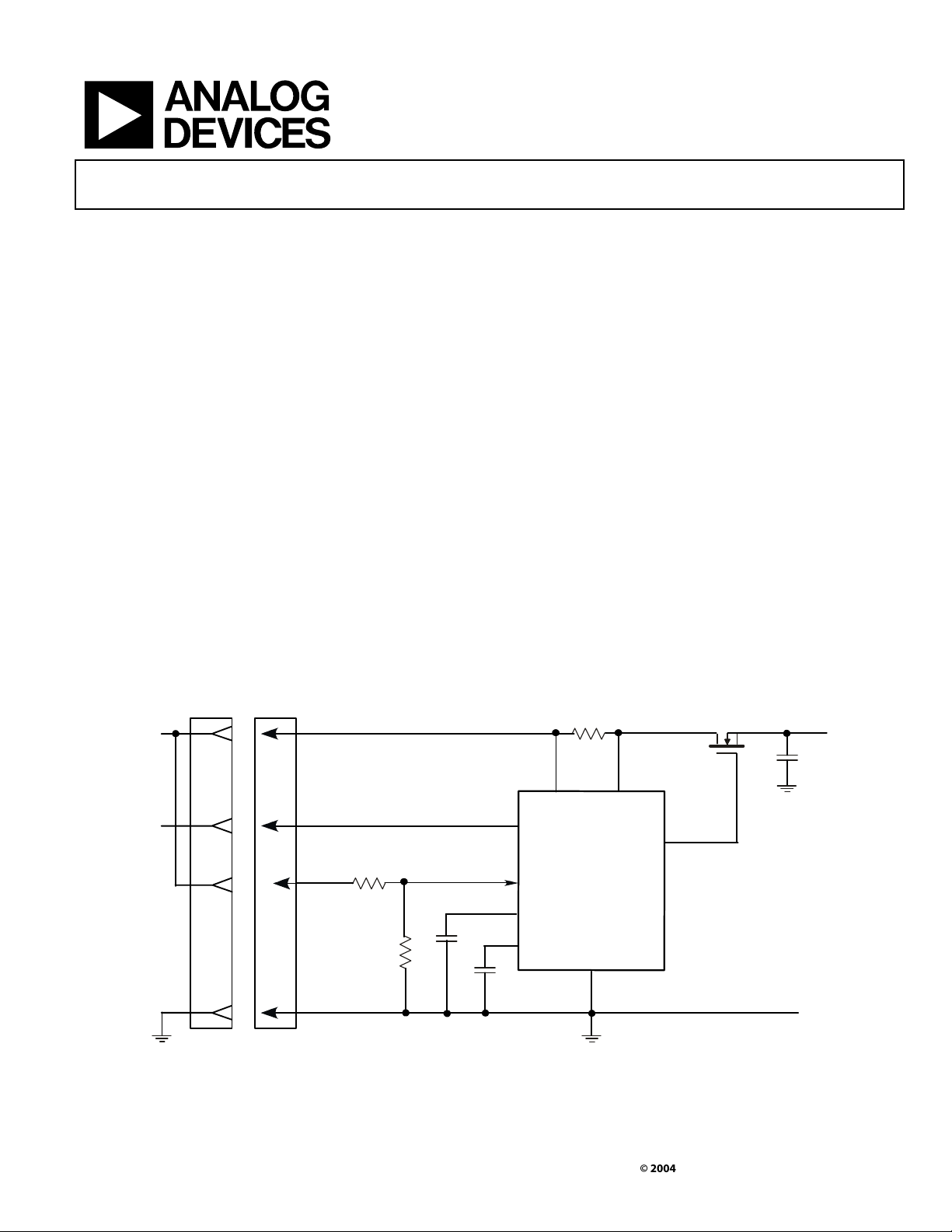
APPLICATIONS DIAGRAM
VIN=1.8V
LONG
Hot Swap Controller
ADM1170
GENERAL DESCRIPTION
The ADM1170 is a Hot Swap controller that allows a board to
be safely inserted and removed from a live backplane. The
device is capable of hot swapping a supply as low as 0.6V.
An internal charge pumped driver controls the GATE of an
external high side N-channel FET for a supply voltage ranging
from 2.7V to 16.5V. The ADM1170 provides the initial timing
cycle and allows the GATE to be ramped up at an adjustable
rate.
The ADM1170 features a fast current limit loop providing
active current limiting together with a circuit breaker timer.
The signal at the ON pin turns the part on and off and is also
used for the reset function.
The SS pin allows the user to control the soft start profile of the
current ramp at start-up via an external capacitor.
A capacitor connected to the TIMER pin gives the user control
over the duty cycle of the PWM retry ratio during current fault.
This part is available in two options: the ADM1170-1 will
automatic retry for over-current fault and the ADM1170-2 will
latch-off for an over-current fault.
The ADM1170 is packaged in an 8-lead TSOT package.
R
SENSE
Q
1
V
OUT
=1.8V
VIN=3.3VAUX
GND
LONG
SHORT
LONG
R
ON1
R
ON2
Rev.PrF
Information furnished by Analog Devices is believed to be accurate and reliable.
However, no responsibility is assumed by Analog Devices for its use, nor for any
infringements of patents or other rights of third parties that may result from its use.
Specifications subject to change without notice. No license is granted by implication
or otherwise under any patent or patent rights of Analog Devices. Trademarks and
registered trademarks are the property of their respective companies.
C
LOAD
RS+
V
cc
RS
-
GATE
ADM1170-1
ON
SS
C
SS
TIMER
C
TIMER
One Technology Way, P.O. Box 9106, Norwood, MA 02062-9106, U.S.A.
Tel: 781.329.4700
Fax: 781.326.8703 © 2004 Analog Devices, Inc. All rights reserved.
GND
GND
www.analog.com

ADM1170 Preliminary Technical Data
ADM1170—SPECIFICATIONS
Table 1. V
Parameter Min Typ Max Units Conditions
VCC Pin
Operating Voltage Range, VCC 2.7 16.5 V
Supply Current, Icc 0.5 1.0
Undervoltage Lockout, V
Undervoltage Lockout Hysteresis, V
ON Pin
ON Pin Input Current, I
On Pin Threshold, VON 1.26 1.3 1.34
ON Pin Threshold Hysteresis, V
RS+/ RS- Pin
Hot Swap Voltage 0.6 16.5
SENSE Pin Input Current, I
Circuit Breaker Limit Voltage, VCB 34 47 60
44 47 53
Over Current Limit Voltage, VOC 40 53 66
50 53 59
GATE Pin
GATE Drive Voltage, V
GATE Drive Voltage, V
GATE Drive Voltage, V
Gate Pullup Current
Gate Pulldown Current
Gate Pulldown Current
Soft Start (SS) Pin
Soft Start Pullup Current 10
Current Setting Gain 20
Soft Start Completion Voltage 1
Pull-Down Current 100
TIMER Pin
TIMER Pin Pull-Up Current, I
-48 -60 -72
TIMER Pin Pull-Down Current, I
100
TIMER Pin Threshold High, V
TIMER Pin Threshold Low, V
= 2.7V to 16.5V, TA = -40°C to +85°C, Typical Values at TA = 25°C unless otherwise noted.
CC
ON rising
V
V
VCB = (V
VCB = (V
V
V
mA
2.4 2.525 2.65 V VCC Rising
UVLO
25
UVLOHYS
mV
INON
-100 0 100
nA
V
80
ONHYST
mV
V
INSENSE
TBD -200 TBD
10 20 30
µA
µA
mV
mV
mV
mV
GATE
6 8 12 V V
GATE
5 6.5 10 V V
GATE
5 6.5 10 V V
10 12 14 uA V
2 mA V
25 mA V
µA
V/V
V
µA
Vss/Vsense
Fault
-4 -5 -6
TIMERUP
µA
µA
TIMERDN
2 2.5
µA
µA
1.235 1.3 1.365
TIMERH
0.18 0.2 0.22
TIMERL
V
V
Initial Cycle, V
During Current Fault, V
After Current Fault, V
Normal Operation, V
TIMER rising
TIMER falling
= VCC, V
SENSE
SENSE
HOTSWAP
HOTSWAP
– VCC, VCC = 2.7V
GATE
– VCC, VCC = 5V
GATE
– VCC, VCC = 16.5V
GATE
= 0V
GATE
= 3V, Vcc > UVLO
GATE
= 3V, Vcc < UVLO
GATE
HOTSWAP
= VCC, V
HOTSWAP
– V
CC
SENSE
– V
CC
SENSE
= 0.6 V, Note
> 2.2 V
TIMER
= 0.6 V, Note
> 2.2 V
) ,V
HOTSWAP
) ,V
HOTSWAP
= 1V
TIMER
= 1V
TIMER
= 1V
TIMER
= 0.6 V
> 2.2 V
= 1V
Rev. PrF | Page 2 of 8

Preliminary Technical Data ADM1170
Absolute Maximum Ratings
Table 2. ADM1170 Absolute Maximum Ratings
Parameter
VCC Pin 20V
RS+, RS- Pins -0.3V to 20V
V
= (RS+ - RS-) 1V
SENSE
TIMER Pin -0.3V to 20V
SS Pin -0.3V to 20V
ON Pin -0.3V to 20V
GATE Pin VCC + 11V
Power Dissipation TBD
Storage Temperature –65°C to +125°C
Operating Temperature Range –40°C to +85°C
Lead Temperature Range (10 sec) 300°C
Junction Temperature 150°C
Rating
Rev. PrF | Page 3 of 8
 Loading...