V
V
V
www.BDTIC.com/ADI
Simple Sequencers® in 6-Lead SC70
FEATURES
Provide programmable time delays between enable
signals
Can be cascaded with power modules for multiple
sup
ply sequencing
Power supply monitoring from 0.6 V
Output stages
High voltage (up to 22 V) open-drain output
ADM1085/ADM1087)
(
Push-pull output (ADM1086/ADM1088)
Capacitor-adjustable time delays
High voltage (up to 22 V) enable and V
Low power consumption (15 μA)
Specified over –40°C to +125°C temperature range
6-lead SC70 package
APPLICATIONS
Desktop/notebook computers, servers
Low power portable equipment
Routers
Base stations
Line cards
Graphics cards
GENERAL DESCRIPTION
inputs
IN
ADM1085/ADM1086/ADM1087/ADM1088
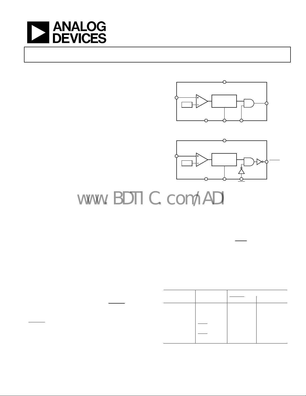
FUNCTIONAL BLOCK DIAGRAMS
CC
ADM1085/ADM1086
GND
GND
CAPACITOR
ADJUSTABLE
DELAY
V
CC
CAPACITOR
ADJUSTABLE
DELAY
Figure 1.
ENOUT
ENINCEXT
ENOUT
ENINCEXT
IN
0.6V
ADM1087/ADM1088
IN
0.6V
04591-001
The ADM1085/ADM1086/ADM1087/ADM1088 are simple
sequencing circuits that provide a time delay between the
enabling of voltage regulators and/or dc-dc converters at powerup in multiple supply systems. When the output voltage of the
first power module reaches a preset threshold, a time delay is
initiated before an enable signal allows subsequent regulators to
power up. Any number of these devices can be cascaded with
regulators to allow sequencing of multiple power supplies.
Threshold levels can be set with a pair of external resistors in a
v
oltage divider configuration. With appropriate resistor values,
the threshold can be adjusted to monitor voltages as low as 0.6 V.
The ADM1086 and ADM1088 have push-pull output stages,
ith active high (ENOUT) and active low (
w
ENOUT
) logic
outputs, respectively. The ADM1085 has an active-high
(ENOUT) logic output; the ADM1087 has an active-low
(
ENOUT
) output. Both the ADM1085 and ADM1087 have
open-drain output stages that can be pulled up to voltage levels
as high as 22 V through an external resistor. This level-shifting
property ensures compatibility with enable input logic levels of
different regulators and converters.
Rev. A
Information furnished by Analog Devices is believed to be accurate and reliable. However, no
responsibility is assumed by Anal og Devices for its use, nor for any infringements of patents or ot her
rights of third parties that may result from its use. Specifications subject to change without notice. No
license is granted by implication or otherwise under any patent or patent rights of Analog Devices.
Trademarks and registered trademarks are the property of their respective owners.
All four models have a dedicated enable input pin that allows
he output signal to the regulator to be controlled externally.
t
This is an active high input (ENIN) for the ADM1085 and
ADM1086, and an active low input (
) for the ADM1087
ENIN
and ADM1088.
The Simple Sequencers are specified over the extended
−40°C t
o +125°C temperature range. With low current
consumption of 15 μA (typical) and 6-lead SC70 packaging,
the parts are suitable for low-power portable applications.
Table 1. Selection Table
Output Stage
Part No. Enable Input
ADM1085 ENIN
ADM1086 ENIN
ADM1087
ADM1088
ENIN
ENIN
ENOUT
Open-drain
Push-pull
ENOUT
Open-drain
Push-pull
One Technology Way, P.O. Box 9106, Norwood, MA 02062-9106, U.S.A.
Tel: 781.329.4700 www.analog.com
Fax: 781.461.3113 ©2006 Analog Devices, Inc. All rights reserved.

ADM1085/ADM1086/ADM1087/ADM1088
www.BDTIC.com/ADI
TABLE OF CONTENTS
Features .............................................................................................. 1
Capacitor-Adjustable Delay Circuit............................................9
Applications....................................................................................... 1
Functional Block Diagrams............................................................. 1
General Description......................................................................... 1
Revision History ............................................................................... 2
Specifications..................................................................................... 3
Absolute Maximum Ratings............................................................ 4
ESD Caution.................................................................................. 4
Pin Configuration and Function Descriptions............................. 5
Typical Performance Characteristics ............................................. 6
Circuit Information.......................................................................... 9
Timing Characteristics and Truth Tables.................................. 9
REVISION HISTORY
4/06—Rev. 0 to Rev. A
Added Lead-Free Models ..................................................Universal
Update Outline Dimensions ......................................................... 15
Changes to Ordering Guide.......................................................... 15
Open-Drain and Push-Pull Outputs ....................................... 10
Application Information................................................................ 11
Sequencing Circuits ................................................................... 11
Dual LOFO Sequencing ............................................................ 13
Simultaneous Enabling .............................................................. 13
Power Good Signal Delays........................................................ 13
Quad-Supply Power Good Indicator....................................... 14
Sequencing with FET Switches................................................. 14
Outline Dimensions ....................................................................... 15
Ordering Guide .......................................................................... 15
7/04—Revision 0: Initial Version
Rev. A | Page 2 of 16

ADM1085/ADM1086/ADM1087/ADM1088
www.BDTIC.com/ADI
SPECIFICATIONS
VCC = full operating range, TA = −40°C to +125°C, unless otherwise noted.
Table 2.
Parameter Min Typ Max Unit Test Conditions/Comments
SUPPLY
VCC Operating Voltage Range 2.25 3.6 V
VIN Operating Voltage Range 0 22 V
Supply Current 10 15 μA
VIN Rising Threshold, V
VIN Falling Threshold, V
TH_RISING
TH_FALLING
VIN Hysteresis 15 mV
VIN to ENOUT/ENOUT Delay
VIN Rising 35 μs CEXT floating, C = 20 pF
2 ms CEXT = 470 pF
VIN Falling 20 μs VIN = V
VIN Leakage Current 170 μA VIN = 22 V
CEXT Charge Current 125 250 375 nA
Threshold Temperature Coefficient 30 ppm/°C
ENIN/ENIN to ENOUT/ENOUT
Propagation Delay
ENIN/ENIN Voltage Low
ENIN/ENIN Voltage High
ENIN/ENIN Leakage Current
ENOUT/ENOUT Voltage Low
ENOUT/ENOUT Voltage High
(ADM1086/ADM1088)
ENOUT/ENOUT Open-Drain Output
Leakage Current (ADM1085/ADM1087)
0.56 0.6 0.64 V VCC = 3.3 V
0.545 0.585 0.625 V VCC = 3.3 V
TH_FALLING
0.5 μs V
0.3 V
0.3 V
+ 0.2 V
CC
− 0.2 V
CC
170 μA
0.4 V
0.8 V
CC
V
0.4 μA
IN
> V
TH_RISING
ENIN/ENIN = 22 V
VIN < V
TH_FALLING
VIN > V
I
= 1.2 mA
SINK
> V
V
IN
V
< V
IN
I
SOURCE
(ENOUT),
TH_RISING
(ENOUT),
TH_RISING
TH_FALLING
= 500 μA
ENOUT/ENOUT = 22 V
to (V
TH_FALLING
(ENOUT),
(ENOUT),
– 100 mV)
Rev. A | Page 3 of 16

ADM1085/ADM1086/ADM1087/ADM1088
www.BDTIC.com/ADI
ABSOLUTE MAXIMUM RATINGS
TA = 25°C, unless otherwise noted.
Table 3.
Parameter Rating
V
CC
V
IN
CEXT
ENIN, ENIN
ENOUT, ENOUT (ADM1085, ADM1087)
ENOUT, ENOUT (ADM1086, ADM1088)
Operating Temperature Range
Storage Temperature Range
θJA Thermal Impedance, SC70 146°C/W
Lead Temperature
Soldering (10 sec) 300°C
Vapor Phase (60 sec) 215°C
Infrared (15 sec) 220°C
−0.3 V to +6 V
−0.3 V to +25 V
−0.3 V to +6 V
−0.3 V to +25 V
−0.3 V to +25 V
−0.3 V to +6 V
−40°C to +125°C
−65°C to +150°C
Stresses above those listed under Absolute Maximum Ratings
ma
y cause permanent damage to the device. This is a stress
rating only; functional operation of the device at these or any
other conditions above those indicated in the operational
section of this specification is not implied. Exposure to absolute
maximum rating conditions for extended periods may affect
device reliability.
ESD CAUTION
ESD (electrostatic discharge) sensitive device. Electrostatic charges as high as 4000 V readily accumulate on the
human body and test equipment and can discharge without detection. Although this product features
proprietary ESD protection circuitry, permanent damage may occur on devices subjected to high energy
electrostatic discharges. Therefore, proper ESD precautions are recommended to avoid performance
degradation or loss of functionality.
Rev. A | Page 4 of 16

ADM1085/ADM1086/ADM1087/ADM1088
www.BDTIC.com/ADI
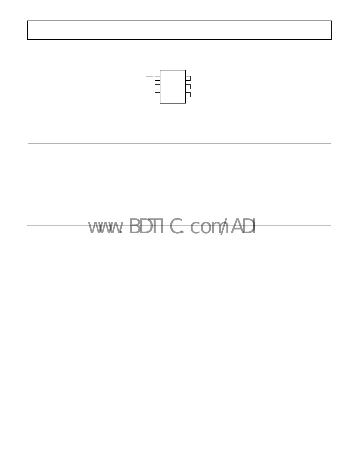
PIN CONFIGURATION AND FUNCTION DESCRIPTIONS
ADM1085/
Table 4. Pin Function Descriptions
Pin No. Mnemonic Description
1
ENIN, ENIN
Enable Input. Controls the status of the enable output. Active high for ADM1085/ADM1086. Active low for
ADM1087/ADM1088.
2 GND Ground.
3 VIN
Input for the Monitored Voltage Signal. Can be biased via a voltage divider resistor network to customize the
ective input threshold. Can precisely monitor an analog power supply output signal and detect when it has
eff
powered up. The voltage applied at this pin is compared with a 0.6 V on-chip reference. With this reference,
digital signals with various logic level thresholds can also be detected.
4
ENOUT, ENOUT
Enable Output. Asserted when the voltage at VIN is above V
that the enable input is asserted. Active high for the ADM1085/ADM1086. Active low for the
ADM1087/ADM1088.
5 CEXT
External Capacitor Pin. The capacitance on this pin determines the time dela
is seen only when the voltage at V
6 VCC Power Supply.
ENIN/ENIN
GND
V
1
ADM1086/
ADM1087/
2
ADM1088
3
TOP VIEW
IN
(Not to Scale)
Figure 2. Pin Configuration
rises past V
IN
6
5
4
V
CC
CEXT
ENOUT/ENOUT
04591-002
and the time delay has elapsed, provided
TH_RISING
, and not when it falls below V
TH_RISING
y on the enable output. The delay
.
TH_FALLING
Rev. A | Page 5 of 16
 Loading...