Super Sequencer™ with
FEATURES
Complete supervisory and sequencing solution for up to
10 supplies
10 supply fault detectors enable supervision of supplies to
better than 1% accuracy
5 selectable input attenuators allow supervision:
Supplies up to 14.4 V on VH
Supplies up to 6 V on VP1–4
5 dual-function inputs, VX1–5:
High impedance input to supply fault detector with
thresholds between 0.573 V and 1.375 V
General-purpose logic input
10 programmable output drivers (PDO1–10):
Open collector with external pull-up
Push/pull output, driven to VDDCAP or VPn
Open collector with weak pull-up to VDDCAP or VPn
Internally charge-pumped high drive for use with external
N-FET (PDO1–6 only)
Sequencing engine (SE) implements state machine control of
PDO outputs:
State changes conditional on input events
Enables complex control of boards
Power-up and power-down sequence control
Fault event handling
Interrupt generation on warnings
Watchdog function can be integrated in SE
Program software control of sequencing through SMBus
12-bit ADC for readback of all supervised voltages
2 auxiliary (single-ended) ADC inputs
Reference input, REFIN, has 2 input options:
Driven directly from 2.048V (±0.25%) REFOUT pin
More accurate external reference for improved ADC
performance
Device powered by the highest of VP1–4, VH for improved
redundancy
User EEPROM: 256 bytes
Industry-standard 2-wire bus interface (SMBus)
Guaranteed PDO low with VH, VPn = 1.2 V
40-lead 6 mm × 6 mm LFCSP and
48-lead 7 mm × 7 mm TQFP packages
Voltage Readback ADC
ADM1064
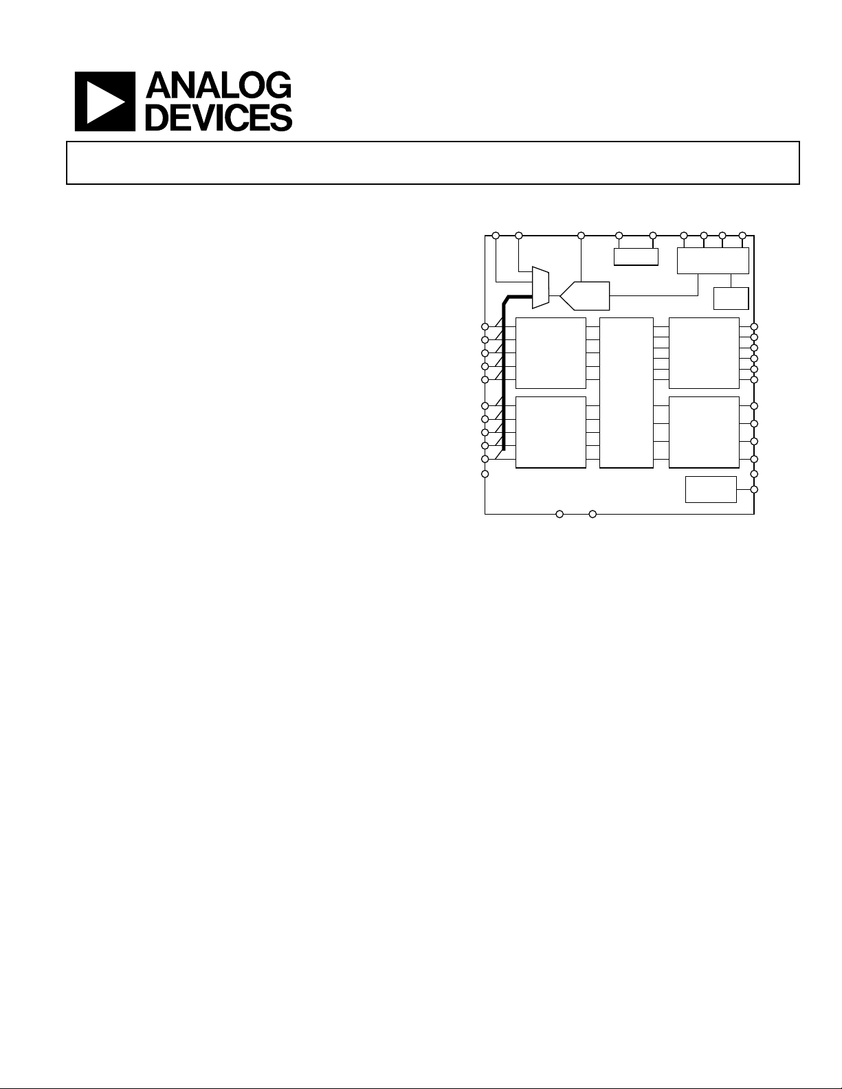
FUNCTIONAL BLOCK DIAGRAM
REFOUTREFINAUX2AUX1 REFGND
VX1
VX2
VX3
VX4
VX5
VP1
VP2
VP3
VP4
AGND
ADM1064
12-BIT
MUX
SAR ADC
DUAL-
FUNCTION
INPUTS
(LOGIC INPUTS
OR
SFDs)
PROGRAMMABLE
RESET
GENERATORS
VH
(SFDs)
GNDVCCP
VREF
SEQUENCING
ENGINE
Figure 1.
APPLICATIONS
Central office systems
Servers/routers
Multivoltage system line cards
DSP/FPGA supply sequencing
In-circuit testing of margined supplies
GENERAL DESCRIPTION
The ADM1064 is a configurable supervisory/sequencing device
that offers a single-chip solution for supply monitoring and
sequencing in multiple supply systems. In addition to these
functions, the ADM1064 integrates a 12-bit ADC which can be
used to accurately read back up to 12 separate voltages.
SDA SCL A1 A0
SMBus
INTERFACE
EEPROM
CONFIGURABLE
OUTPUT
DRIVERS
(HV CAPABLE
OF DRIVING
GATES OF
N-CHANNEL FET)
CONFIGURABLE
OUTPUT
DRIVERS
(LV CAPABLE
OF DRIVING
LOGIC SIGNALS)
VDD
ARBITRATOR
PDO1
PDO2
PDO3
PDO4
PDO5
PDO6
PDO7
PDO8
PDO9
PDO10
PDOGND
VDDCAP
(continued on Page 3)
04633-001
Rev. A
Information furnished by Analog Devices is believed to be accurate and reliable.
However, no responsibility is assumed by Analog Devices for its use, nor for any
infringements of patents or other rights of third parties that may result from its use.
Specifications subject to change without notice. No license is granted by implication
or otherwise under any patent or patent rights of Analog Devices. Trademarks and
registered trademarks are the property of their respective owners.
One Technology Way, P.O. Box 9106, Norwood, MA 02062-9106, U.S.A.
Tel: 781.329.4700
Fax: 781.326.8703 © 2005 Analog Devices, Inc. All rights reserved.
www.analog.com

ADM1064
TABLE OF CONTENTS
General Description......................................................................... 3
Sequencing Engine Application Example ............................... 18
Specifications..................................................................................... 4
Pin Configurations and Function Descriptions ........................... 7
Absolute Maximum Ratings............................................................ 8
Thermal Characteristics .............................................................. 8
ESD Caution.................................................................................. 8
Typical Performance Characteristics............................................. 9
Powering the ADM1064................................................................ 12
Inputs................................................................................................ 13
Supply Supervision .....................................................................13
Programming the Supply Fault Detectors............................... 13
Input Comparator Hysteresis.................................................... 14
Input Glitch Filtering ................................................................. 14
Supply Supervision with VXn Inputs....................................... 14
VXn Pins as Digital Inputs........................................................ 15
Outputs ............................................................................................ 16
Sequence Detector...................................................................... 19
Monitoring Fault Detector ........................................................ 19
Timeout Detector ....................................................................... 19
Fault Reporting ........................................................................... 19
Volt a ge R e ad b ac k ............................................................................ 20
Supply Supervision with the ADC ........................................... 20
Applications Diagram .................................................................... 21
Communicating with the ADM1064........................................... 22
Configuration Download at Power-Up................................... 22
Updating the Configuration ..................................................... 22
Updating the Sequencing Engine............................................. 23
Internal Registers........................................................................ 23
EEPROM ..................................................................................... 23
Serial Bus Interface..................................................................... 23
SMBus Protocols for RAM and EEPROM.............................. 25
Supply Sequencing through Configurable Output Drivers .. 16
Sequencing Engine......................................................................... 17
Overview...................................................................................... 17
Wa r ni n g s ...................................................................................... 17
SMBus Jump/Unconditional Jump .......................................... 17
REVISION HISTORY
1/05—Rev. 0 to Rev A
Changes to Figure 1.......................................................................... 1
Changes to Absolute Maximum Ratings Section ......................... 8
Change to Supply Sequencing through Configurable
Output Drivers Section............................................................... 16
Changes to Figure 33...................................................................... 21
Change to Table 9 ........................................................................... 24
10/04—Revision 0: Initial Version
Write Operations........................................................................ 25
Read Operations......................................................................... 27
Outline Dimensions....................................................................... 29
Ordering Guide .......................................................................... 29
Rev. A | Page 2 of 32
ADM1064
GENERAL DESCRIPTION
(continued from Page 1)
The device also provides up to ten programmable inputs for
monitoring under, over, or out-of-window faults on up to ten
supplies. In addition, ten programmable outputs can be use d as
logic enables. Six of them can also provide up to a 12 V output
for driving the gate of an N-channel FET, which can be placed
in the path of a supply.
The logical core of the device is a sequencing engine. This statemachine-based construction provides up to 63 different states.
REFOUTREFINAUX1AUX2 REFGND
This design enables very flexible sequencing of the outputs,
based on the condition of the inputs.
The device is controlled via configuration data that can be
programmed into an EEPROM. The whole configuration can
be programmed using an intuitive GUI-based software package
provided by ADI.
SDA SCL A1 A0
VX1
VX2
VX3
VX4
VX5
VP1
VP2
VP3
VP4
VH
AGND
VDDCAP
SELECTABLE
ATTENUATOR
SELECTABLE
ATTENUATOR
VDD
ARBITRATOR
ADM1064
SAR ADC
GPI SIGNAL
CONDITIONING
GPI SIGNAL
CONDITIONING
REG 5.25V
CHARGE PUMP
12-BIT
SFD
SFD
SFD
SFD
VREF
INTERFACE
CONTROLLER
SEQUENCING
ENGINE
SMBus
DEVICE
OSC
EEPROM
CONFIGURABLE
O/P DRIVER
(HV)
CONFIGURABLE
O/P DRIVER
(HV)
CONFIGURABLE
O/P DRIVER
(LV)
CONFIGURABLE
O/P DRIVER
(LV)
PDO1
PDO2
PDO3
PDO4
PDO5
PDO6
PDO7
PDO8
PDO9
PDO10
PDOGND
VCCPGND
04633-002
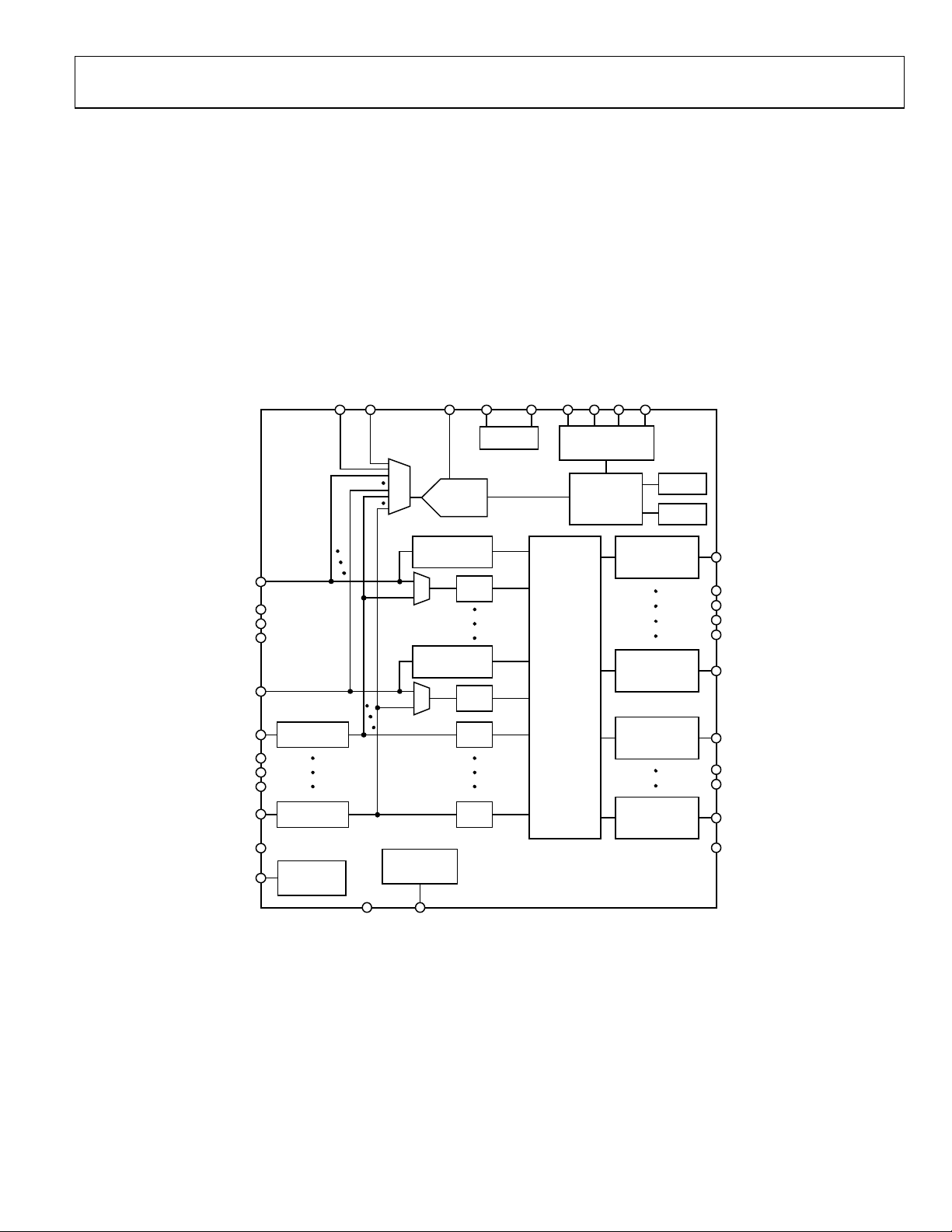
Figure 2. Detailed Block Diagram
Rev. A | Page 3 of 32

ADM1064
SPECIFICATIONS
VH = 3.0 V to 14.4 V1, VPn = 3.0 V to 6.0 V1, TA = −40°C to +85°C, unless otherwise noted.
Table 1.
Parameter Min Typ Max Unit Test Conditions/Comments
POWER SUPPLY ARBITRATION
VH, VPn 3.0 V Minimum supply required on one of VPn, VH
VP 6.0 V Maximum VDDCAP = 5.1 V, typical
VH 14.4 V VDDCAP = 4.75 V
VDDCAP 2.7 4.75 5.4 V Regulated LDO output
C
VDDCAP
POWER SUPPLY
Supply Current, IVH, I
Additional Currents
All PDO FET Drivers On 1 mA
Current Available from VDDCAP 2 mA
DACs Supply Current 2.2 mA 6 DACs on with 100 µA maximum load on each
ADC Supply Current 1 mA Running round-robin loop
EEPROM Erase Current 10 mA 1 ms duration only, VDDCAP = 3 V
SUPPLY FAULT DETECTORS
VH Pin
Input Attenuator Error ±0.05 % Midrange and high range
Detection Ranges
High Range 6 14.4 V
Midrange 2.5 6 V
VPn Pins
Input Attenuator Error ±0.05 % Low range and midrange
Detection Ranges
Midrange 2.5 6 V
Low Range 1.25 3 V
Ultralow Range 0.573 1.375 V No input attenuation error
VX Pins
Input Impedance 1 MΩ
Detection Ranges
Ultralow Range 0.573 1.375 V No input attenuation error
Absolute Accuracy ±1 %
Threshold Resolution 8 Bits
Digital Glitch Filter 0 µs Minimum programmable filter length
100 µs Maximum programmable filter length
ANALOG-TO-DIGITAL CONVERTER
Signal Range 0 V
VPn
10 µF Minimum recommended decoupling capacitance
4.2 6 mA VDDCAP = 4.75 V, PDO1–10 off, DACs off, ADC off
VDDCAP = 4.75 V, PDO1-6 loaded with 1 µA each,
PDO7–10 off
Maximum additional load that can be drawn from
all PDO pull-ups to VDDCAP
VREF error + DAC nonlinearity + comparator offset
error + input attenuation error
REFIN
V
The ADC can convert signals presented to the VH,
VPn, and VX_GPIn pins. VPn and VH input signals
are attenuated depending on selected range. A
signal at the pin corresponding to the selected
range is from 0.573 V to 1.375 V at the ADC input.
Rev. A | Page 4 of 32

ADM1064
Parameter Min Typ Max Unit Test Conditions/Comments
Input Reference Voltage on REFIN Pin,
V
REFIN
Resolution 12 Bits
INL ±2.5 LSB Endpoint corrected, V
Gain Error ±0.05 % V
Conversion Time 0.44 ms One conversion on one channel
84 ms All 12 channels selected, 16x averaging enabled
Offset Error ±2 LSB V
Input Noise 0.25 LSB
REFERENCE OUTPUT
Reference Output Voltage 2.043 2.048 2.053 V No load
Load Regulation −0.25 mV Sourcing current, I
0.25 mV Sinking current, I
Minimum Load Capacitance 1 µF Capacitor required for decoupling, stability
Load Regulation 2 mV Per 100 µA
PSRR 60 dB DC
PROGRAMMABLE DRIVER OUTPUTS
High Voltage (Charge Pump) Mode
(PDO1–6)
Output Impedance 500 kΩ
V
OH
10.5 12 13.5 V IOH = 1 µA
I
OUTAVG
Standard (Digital Output) Mode (PDO1–10)
V
OH
4.5 V VPU to Vpn = 6.0 V, IOH = 0 mA
V
V
OL
I
OL2
2
I
60 mA Maximum total sink for all PDOs
SINK
R
PULL-UP
I
(VPn)2 2 mA
SOURCE
Three-State Output Leakage Current 10 µA V
Oscillator Frequency 90 100 110 kHz All on-chip time delays derived from this clock
DIGITAL INPUTS (VXn, A0, A1)
Input High Voltage, V
Input Low Voltage, V
Input High Current, I
Input Low Current, I
IH
IL
IH
IL
Input Capacitance 5 pF
Programmable Pull-Down Current,
I
PULL-DOWN
SERIAL BUS DIGITAL INPUTS (SDA, SCL)
Input High Voltage, V
Input Low Voltage, V
Output Low Voltage, V
IH
IL
2
0.4 V I
OL
2.048 V
= 2.048 V
REFIN
= 2.048 V
REFIN
= 2.048 V
REFIN
Direct input (no attenuator)
rms
= −100 µA
DACnMAX
= 100 µA
DACnMAX
11 12.5 14 V IOH = 0
20 µA 2 V < V
OH
< 7 V
2.4 V VPU (pull-up to VDDCAP or VPN) = 2.7 V, IOH = 0.5 mA
− 0.3 V VPU ≤ 2.7 V, IOH = 0.5 mA
PU
0 0.50 V IOL = 20 mA
20 mA Maximum sink current per PDO pin
20 kΩ Internal pull-up
Current load on any VPn pull-ups, that is, total
source current available through any number of
PDO pull-up switches configured onto any one
= 14.4 V
PDO
2.0 V Maximum VIN = 5.5 V
0.8 V Maximum VIN = 5.5 V
−1 µA VIN = 5.5 V
1 µA VIN = 0
20 µA
VDDCAP = 4.75, T
= 25°C, if known logic state is
A
required
2.0 V
0.8 V
= −3.0 mA
OUT
Rev. A | Page 5 of 32

ADM1064
Parameter Min Typ Max Unit Test Conditions/Comments
SERIAL BUS TIMING
Clock Frequency, f
Bus Free Time, t
Start Setup Time, t
Start Hold Time, t
SCL Low Time, t
SCL High Time, t
SCL, SDA Rise Time, t
SCL, SDA Fall Time, t
Data Setup Time, t
Data Hold Time, t
Input Low Current, I
SCLK
BUF
SU;STA
HD;STA
LOW
HIGH
r
f
SU;DAT
HD;DAT
IL
SEQUENCING ENGINE TIMING
State Change Time 10 µs
1
At least one of the VH, VP1-4 pins must be ≥ 3.0 V to maintain the device supply on VDDCAP.
2
Specification is not production tested, but is supported by characterization data at initial product release.
400 kHz
4.7 µs
4.7 µs
4 µs
4.7 µs
4 µs
1000 µs
300 µs
250 ns
5 ns
1 µA VIN = 0
Rev. A | Page 6 of 32
ADM1064
V
V
V
V
V
V
V
V
V
V
V
V
V
V
V
V
V
V
PIN CONFIGURATIONS AND FUNCTION DESCRIPTIONS
GND40VDDCAP39AUX138AUX237SDA36SCL35A134A033VCCP32PDOGND
X1
1
PIN 1
INDICATOR
2
X2
3
X3
X4
4
X5
5
P1
6
7
P2
8
P3
P4
9
VH
10
11
12
AGND
NC = NO CONNECT
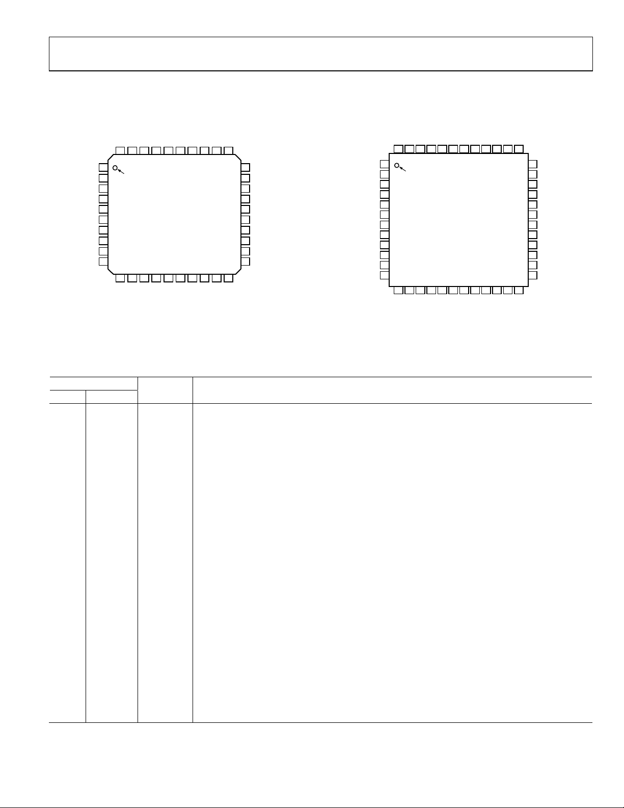
Figure 3. LFCSP Pin Configuration
ADM1064
TOP VIEW
(Not to Scale)
13
14NC15NC16NC17NC18NC19NC20
REFIN
REFOUT
REFGND
31
30
29
28
27
26
25
24
23
22
21
PDO1
PDO2
PDO3
PDO4
PDO5
PDO6
PDO7
PDO8
PDO9
PDO10
04633-003
NC
X1
X2
X3
X4
X5
P1
P2
P3
P4
VH
NC
NC = NO CONNECT
NC48GND47VDDCAP46AUX145AUX244SDA43SCL42A141A040VCCP39PDOGND38NC
1
PIN 1
2
INDICATOR
3
4
5
6
7
8
9
10
11
12
13
14
NC
ADM1064
TOP VIEW
(Not to Scale)
15
16
17NC18NC19NC20NC21NC22NC23NC24
AGND
REFIN
REFOUT
REFGND
Figure 4. TQFP Pin Configuration
37
NC
36
PDO1
35
PDO2
34
PDO3
33
32
PDO4
31
PDO5
30
PDO6
29
PDO7
28
PDO8
27
PDO9
26
PDO10
NC
25
04633-004
Table 2. Pin Function Descriptions
Pin No.
LFCSP TQFP
15-20
1, 12–13,
Mnemonic Description
NC No Connection.
18–25,
36–37, 48
1–5 2–6 VX1–5
High Impedance Inputs to Supply Fault Detectors. Fault thresholds can be set from 0.573 V to 1.375 V.
Alternatively, these pins can be used as general-purpose digital inputs.
6–9 7–10 VP1–4
Low Voltage Inputs to Supply Fault Detectors. Three input ranges can be set by altering the input
attenuation on a potential divider connected to these pins, the output of which connects to a supply
fault detector. These pins allow thresholds from 2.5 V to 6.0 V, 1.25 V to 3.00 V, and 0.573 V to 1.375 V.
10 11 VH
High Voltage Input to Supply Fault Detectors. Three input ranges can be set by altering the input
attenuation on a potential divider connected to this pin, the output of which connects to a supply
fault detector. This pin allows thresholds from 6.0 V to 14.4 V and 2.5 V to 6.0 V.
11 14 AGND Ground Return for Input Attenuators.
12 15 REFGND Ground Return for On-Chip Reference Circuits.
13 16 REFIN Reference Input for ADC. Nominally, 2.048 V.
14 17 REFOUT 2.048 V Reference Output.
21–30 26–35 PDO10–1 Programmable Output Drivers.
31 38 PDOGND Ground Return for Output Drivers.
32 39 VCCP
Central Charge-Pump Voltage of 5.25 V. A reservoir capacitor must be connected between this pin
and GND.
33 40 A0 Logic Input. This pin sets the seventh bit of the SMBus interface address.
34 41 A1 Logic Input. This pin sets the sixth bit of the SMBus interface address.
35 42 SCL SMBus Clock Pin. Open-drain output requires external resistive pull-up.
36 43 SDA SMBus Data I/O Pin. Open-drain output requires external resistive pull-up.
37 44 AUX2 Auxiliary, Single-Ended ADC Input.
38 45 AUX1 Auxiliary, Single-Ended ADC Input.
39 46 VDDCAP Device Supply Voltage. Linearly regulated from the highest of the VP1–4, VH pins to a typical of 4.75 V.
40 47 GND Supply Ground.
Rev. A | Page 7 of 32

ADM1064
ABSOLUTE MAXIMUM RATINGS
Table 3.
Parameter Rating
Voltage on VH Pin 16 V
Voltage on VP Pins 7 V
Voltage on VX Pins −0.3 V to +6.5 V
Voltage on AUX1, AUX2, REFIN Pins −0.3 V to +5 V
Input Current at Any Pin ±5 mA
Package Input Current ±20 mA
Maximum Junction Temperature (TJ max) 150°C
Storage Temperature Range −65°C to +150°C
Lead Temperature, Soldering
Vapor Phase, 60 sec 215°C
ESD Rating 2000 V
ESD CAUTION
ESD (electrostatic discharge) sensitive device. Electrostatic charges as high as 4000 V readily accumulate on
the human body and test equipment and can discharge without detection. Although this product features
proprietary ESD protection circuitry, permanent damage may occur on devices subjected to high energy
electrostatic discharges. Therefore, proper ESD precautions are recommended to avoid performance
degradation or loss of functionality.
Stresses above those listed under Absolute Maximum Ratings
may cause permanent damage to the device. This is a stress
rating only; functional operation of the device at these or any
other conditions above those indicated in the operational
section of this specification is not implied. Exposure to absolute
maximum rating conditions for extended periods may affect
device reliability.
THERMAL CHARACTERISTICS
40-lead LFCSP package: θJA = 25°C/W.
48-lead TQFP package: θ
= 14.8°C/W.
JA
Rev. A | Page 8 of 32
ADM1064
TYPICAL PERFORMANCE CHARACTERISTICS
6
5
4
(V)
3
VDDCAP
V
2
1
0
0654321
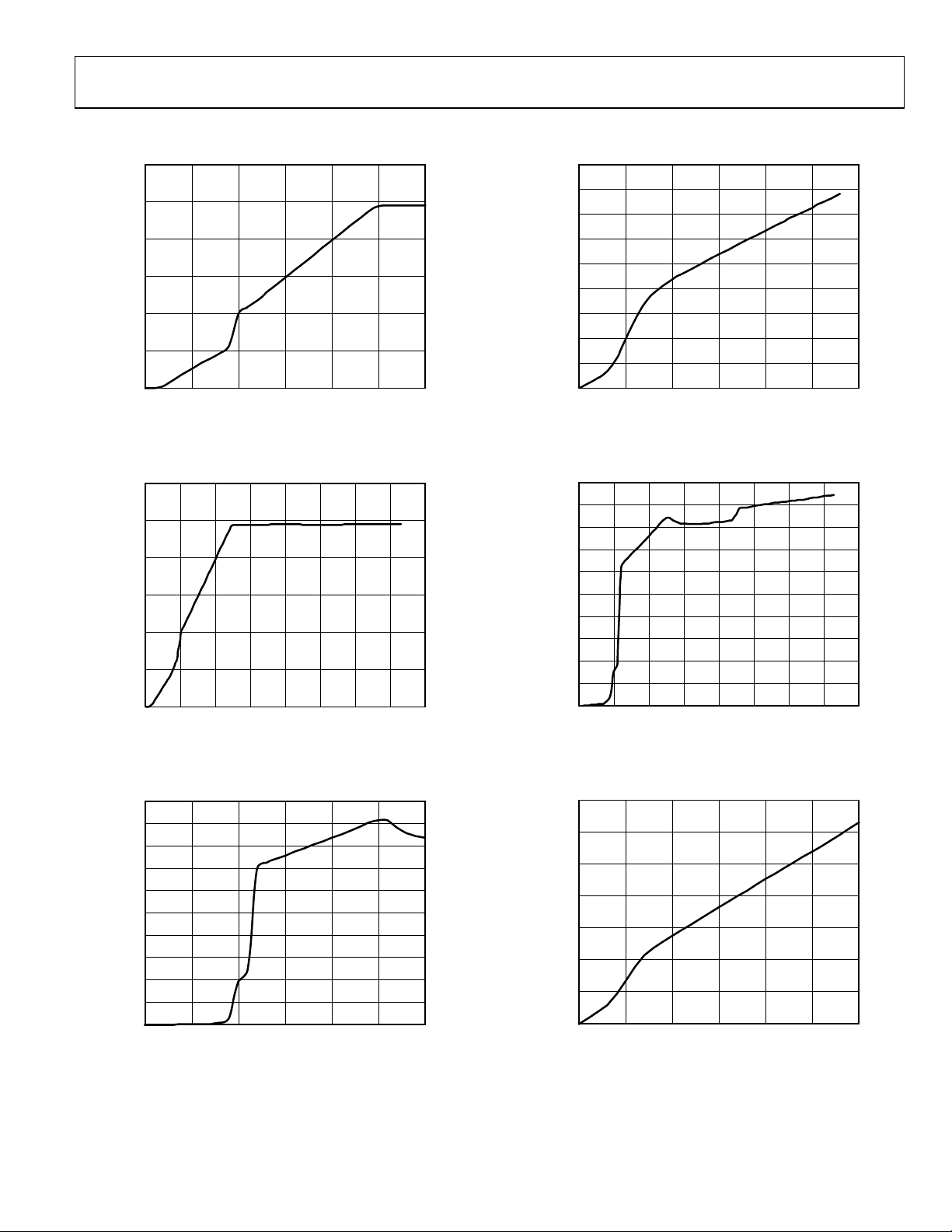
Figure 5. V
V
VP1
VDDCAP
(V)
vs. V
VP1
6
5
4
(V)
3
VDDCAP
V
2
1
0
0161412108642
Figure 6. V
VVH (V)
VDDCAP
vs. V
VH
5.0
4.5
4.0
3.5
3.0
2.5
(mA)
VP1
I
2.0
1.5
1.0
0.5
0
0123456
Figure 7. I
V
(V)
VP1
vs. V
VP1
(VP1 as Supply)
VP1
04633-050
04633-051
04633-052
180
160
140
120
100
A)
µ
(
80
VP1
I
60
40
20
0
0123456
Figure 8. I
V
(V)
VP1
vs. V
VP1
(VP1 Not as Supply)
VP1
5.0
4.5
4.0
3.5
3.0
2.5
(mA)
VH
I
2.0
1.5
1.0
0.5
0
0161412108642
Figure 9. I
VVH (V)
vs. VVH (VH as Supply)
VH
350
300
250
200
(µA)
VH
150
I
100
50
0
0654321
Figure 10. I
VH
vs. V
VH
VVH (V)
(VH Not as Supply)
04633-053
04633-054
04633-055
Rev. A | Page 9 of 32
ADM1064
CHARGE PUMPED
PDO1
V
5.0
4.5
4.0
3.5
3.0
(V)
2.5
PDO1
V
2.0
1.5
1.0
0.5
4.5
4.0
3.5
3.0
2.5
(V)
2.0
PDO1
V
1.5
1.0
0.5
14
12
10
8
6
4
2
0
0 15.012.510.07.55.02.5
0
0654321
0
0605040302010
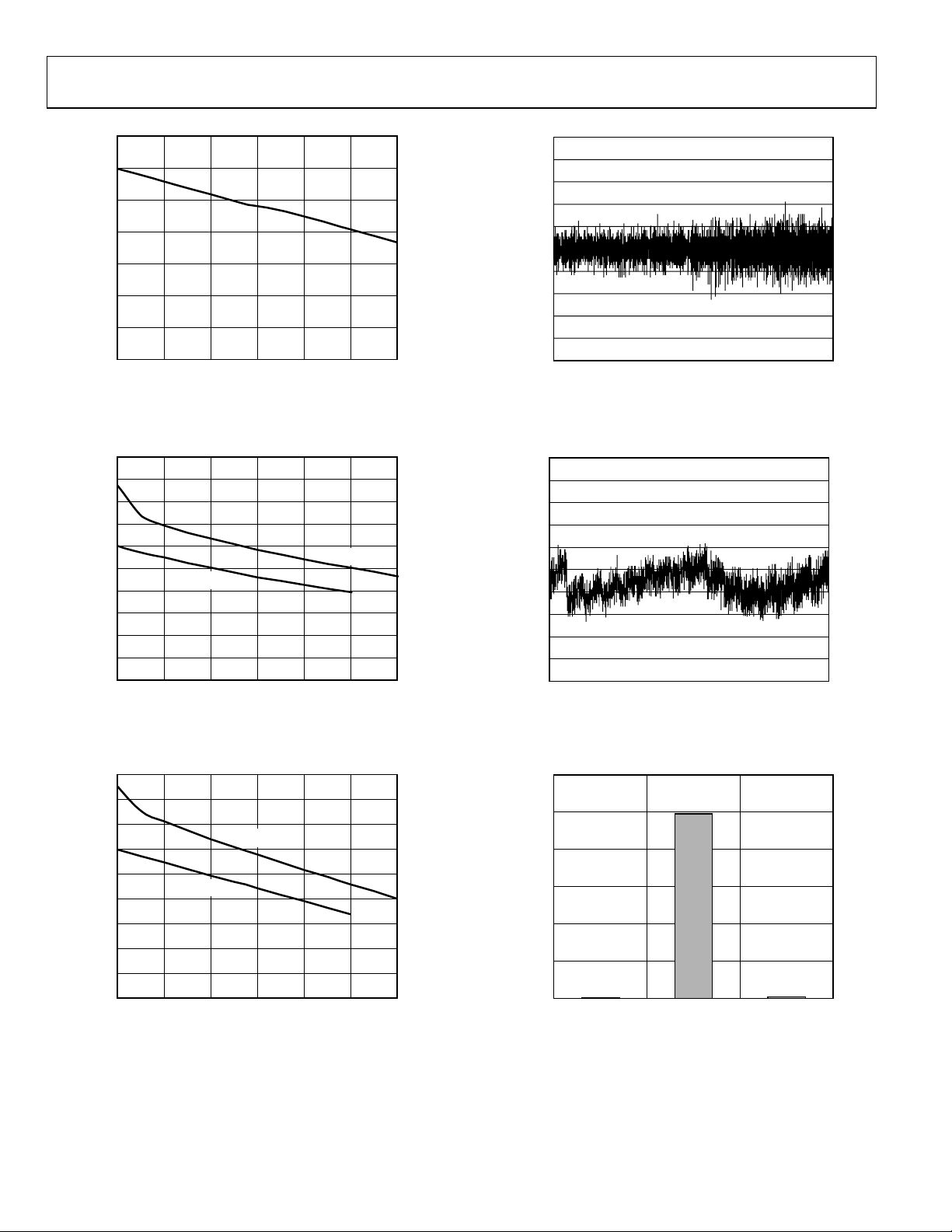
Figure 11. V
Figure 12. V
Figure 13. V
I
CURRENT (µA)
LOAD
(FET Drive Mode) vs. I
PDO1
VP1 = 3V
I
(mA)
LOAD
(Strong Pull-Up VP) vs. I
PDO1
VP1 = 5V
VP1 = 3V
I
(µA)
LOAD
(Weak Pull-Up to VP) vs. I
PDO1
04633-056
LOAD
VP1 = 5V
04633-057
LOAD
04633-058
LOAD
1.0
0.8
0.6
0.4
0.2
0
–0.2
DNL (LSB)
–0.4
–0.6
–0.8
–1.0
CODE
Figure 14. DNL for ADC
1.0
0.8
0.6
0.4
0.2
0
INL (LSB)
–0.2
–0.4
–0.6
–0.8
–1.0
0 4000300020001000
CODE
Figure 15. INL for ADC
12000
10000
8000
6000
HITS PER CODE
4000
2000
0
25
9894
CODE
Figure 16. ADC Noise, Midcode Input, 10,000 Reads
04633-066
40001000 2000 30000
04633-063
81
204920482047
04633-064
Rev. A | Page 10 of 32
 Loading...