Multisupply Supervisor/Sequencer with Margining
Control and Temperature Monitoring
Preliminary Technical Data
FEATURES
10 supply fault detectors enabling supervision of supplies to
better than 1% accuracy
5 selectable input attenuators allow supervision:
Supplies up to 14.4 V on VH
Supplies up to 6 V on VP1-4
5 dual function inputs VX1-5:
High impedance input to supply fault detector with
thresholds between 0.573 V and 1.375 V
General-purpose logic input
Device powered by the highest of VP1–4, VH
2.048 V reference (±0.25%) on REFOUT pin
12-bit ADC for read-back of all supervised voltages
Reference input, REFIN—2 input options:
Driven directly from REFOUT
More accurate external reference for improved ADC
performance
6 voltage output 8-bit DACs (0.300 V to 1.551 V)
Internal temperature sensor
Remote temperature sensor
10 programmable output drivers (PDO1-10)
Open collector with external pull-up
Push-pull output, driven to VDDCAP or VPn
Open collector with weak pull-up to VDDCAP or VPn
Internally charge pumped high drive for use with external
N-FET (PDO1–6 only)
Sequencing Engine (SE) implements State Machine control
of PDO outputs:
State changes conditional on input events
Can enable complex control of boards
Power up and power down sequence control
Fault event handling
Interrupt generation on warnings
Watchdog function can be integrated in SE
Program software control of sequencing through SMBus
User EEPROM—256 Bytes
Industry standard 2-wire bus interface (SMBus)
Guaranteed PDO low with VH, VPn = 1.2V
40-lead LFCSP and 48-lead TQFP packages
ADM1062
APPLICATIONS
Central office systems
Servers/routers
Multivoltage system line cards
DSP/FPGA supply sequencing
In circuit testing of margined supplies
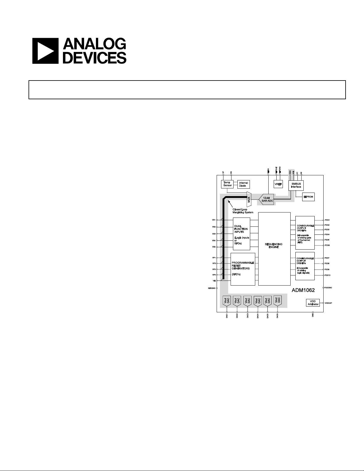
FUNCTIONAL BLOCK DIAGRAM
Figure 1.
GENERAL DESCRIPTION
The ADM1062 is a configurable supervisory/sequencing device
which offers a single chip solution for supply monitoring and
sequencing in multiple supply systems.
(continued on Page 3)
Rev. PrJ
Information furnished by Analog Devices is believed to be accurate and reliable.
However, no responsibility is assumed by Analog Devices for its use, nor for any
infringements of patents or other rights of third parties that may result from its use.
Specifications subject to change without notice. No license is granted by implication
or otherwise under any patent or patent rights of Analog Devices. Trademarks and
registered trademarks are the property of their respective owners.
One Technology Way, P.O. Box 9106, Norwood, MA 02062-9106, U.S.A.
Tel: 781.329.4700
Fax: 781.326.8703 © 2003 Analog Devices, Inc. All rights reserved.
www.analog.com

ADM1062 Preliminary Technical Data
TABLE OF CONTENTS
General Description......................................................................... 3
Timeout Detector ....................................................................... 21
ADM1062 Specifications................................................................. 5
Pin Configurations and Functional Descriptions ........................ 8
Absolute Maximum Ratings............................................................ 9
Thermal Characteristics .............................................................. 9
ESD Caution.................................................................................. 9
Typical Performance Characteristics........................................... 10
ADM1062 Inputs............................................................................ 13
Powering the ADM1062............................................................ 13
Supply Supervision .....................................................................14
Input Comparator Hysteresis.................................................... 14
Input Glitch Filtering ................................................................. 14
Supply Supervision with VXN Inputs...................................... 15
Supply Supervision Using the ADC .........................................15
VXN Pins as Digital Inputs....................................................... 16
ADM1062 Outputs......................................................................... 17
Closed Loop Supply Margining................................................ 21
Writ i ng to t he DACs .................................................................. 22
Choosing the Size of the Feedback Resistor ........................... 22
DAC Limiting/Other Safety Features ...................................... 22
Temperature Measurement System.............................................. 23
Remote Temperature Measurement ........................................ 23
Communicating with the ADM1062........................................... 25
Configuration Download at Power-Up................................... 25
Updating the Configuration of the ADM1062....................... 25
Updating the Sequencing Engine of the ADM1062.............. 26
Internal Registers of the ADM1062......................................... 26
ADM1062 EEPROM.................................................................. 26
Serial Bus Interface..................................................................... 27
Identifying the ADM1062 on the SMBUS.............................. 27
General SMBUS Timing............................................................ 27
ADM1062 Sequencing Engine...................................................... 19
Wa r ni n g s ...................................................................................... 19
SW Flow-Unconditional Jump ................................................. 19
End of Step Detector .................................................................. 20
Monitoring Fault Detector ........................................................ 20
REVISION HISTORY
Revision PrJ: Preliminary Version
SMbus Protocols for RAM and EEPROM .............................. 27
ADM1062 WRITE Operations................................................. 29
ADM1062 READ Operations................................................... 30
Outline Dimensions....................................................................... 32
Ordering Guide .......................................................................... 32
Rev. PrJ | Page 2 of 32

Preliminary Technical Data ADM1062
GENERAL DESCRIPTION
(continued from Page 1)
In addition to these functions the ADM1062 integrates a 12-bit
ADC and six 8-bit voltage output DACs. These circuits can be
used to implement a closed loop margining system. This
enables supply adjustment by altering either the feedback node
or reference of a DC/DC Converter using the DAC outputs. The
supply margining can be performed, with a minimum of
external components, to an accuracy of 0.5%. The margining
loop can be used at In Circuit Testing of a board during
production (to verify the board’s functionality at say −5% of
nominal supplies), or can be used dynamically to accurately
control the output voltage of a DC/DC converter.
up to a +12V output for driving the gate of an N- Channel FET
which may be placed in the path of a supply.
Temperature measurement is possible with the ADM1062. The
device contains one internal temperature sensor and a
differential input for a remote thermal diode. These are
measured using the 12- bit ADC.
The logical core of the device is a Sequencing Engine. This is a
state machine based construction, providing up to 63 different
states. This enables very flexible sequencing of the outputs,
based on the condition of the inputs.
The device also provides up to ten programmable inputs for
monitoring Under, Over, or out-of-window faults on up to ten
supplies. In addition, ten programmable outputs are provided.
These can be used as logic enables. Six of them can also provide
The device is controlled via configuration data which can
programmed into an EEPROM. All of this configuration can be
programmed using an intuitive GUI based software package
provided by ADI.
Rev. PrJ | Page 3 of 32

ADM1062 Preliminary Technical Data
Figure 2. Detailed Block Diagram
Rev. PrJ | Page 4 of 32

Preliminary Technical Data ADM1062
ADM1062 SPECIFICATIONS
VH = 3.0 V to 14.4 V, VPn = 3.0 V to 6.0 V2, TA = −40°C to 85°C, unless otherwise noted.
Table 1.
Parameter Min Typ Max Unit Test Conditions/Comments
POWER SUPPLY ARBITRATION
VH, VPn 3.0 V Min. of VDDCAP=2.7V required
VP 6.0 V Max VDDCAP= 5.1V, Typical
VH 14.4 V VDDCAP = 4.75V
POWER SUPPLY
Supply Current, IVH, I
Temp Sensor and ADC off) 6 mA
Additional Currents
All PDO FET Drivers on 4 mA VDDCAP=4.75V, (loaded with 1µA), no PDO pullups to VDDCAP.
Current available from
VDDCAP
DAC’s Supply Current 2 mA 6 DAC’s on with 100µA max load on each
ADC Supply Current 1 mA Running Round Robin loop
EEPROM Erase Current 10 mA 1ms duration only
SUPPLY FAULT DETECTORS VH
Pin
Input Impedance 26.7 kΩ From VH to GND
Input attenuator error 0.25 % Low, Mid and High ranges on VH, VPn
Detection Ranges
High Range 6 14.4 V
Mid Range 2.5 6 V
VPn Pins
Input Impedance 80 kΩ From VPn to GND
Detection Ranges
Mid Range 2.5 6 V
Low Range 1.25 3 V
Ultra Low Range 0.573 1.375 V
VX Pins
Input Impedance 1 MΩ
Detection Ranges
Ultra Low Range 0.573 1.375 V
Absolute Accuracy 1 % Input attenuator error +
Vref Error + DAC Non Linearity +
Comparator Offset Error
Threshold Resolution 8 bits
Digital Glitch Filter 0 100 µs See Figure x. 8 filter length options
Temperature Sensor
Local Sensor Accuracy ±2 °C
Remote Sensor Accuracy ±2 °C 0°C <= T
Remote Sensor Source Current 200 µA High Level
12 µA Low Level
Temperature for 800h code out 0 °C
Temperature for C00h code out 128 °C
(DAC’s,
VPn
1
VDDCAP=4.75V, no PDO FET Drivers on, no loaded PDO pullups
to VDDCAP
2 mA
Max. additional load that can be drawn from PDO pullups to
VDDCAP
Die temp higher than ambient due to ADM1062 power
consumption
DIODE
<=120°C
Rev. PrJ | Page 5 of 32

ADM1062 Preliminary Technical Data
Parameter Min Typ Max Unit Test Conditions/Comments
Analog to Digital Converter
Signal Range 0 V
Input reference voltage on
2.048 TBD V VDDCAP=2.7V
REFIN
REFIN pin, VREFIN
TBD V VDDCAP=4.75V
Resolution 12 bits
INL ±1.5 lsb End-point corrected, V
DNL ±1 lsb V
Gain Error ±2 lsb V
Offset Error ±2 lsb V
Input Noise 0.25 lsb
Buffered voltage output DACs
Resolution 8 bits
Code 80h output voltage
Range 1 0.6 V
Range 2 0.8 V
Range 3 1 V
Range 4 1.25 V
Output voltage range 601.25 mV Same range independent of centre point
lsb step size 2.36 mV
INL 0.25 lsb
DNL 0.2 lsb
Mid code error 0.5 lsb
Gain Error 0.4 %
Max Load Current (source) 100 µA
Max Load Current(sink) 100 C
Max load Capacitance 50 pF
Settling time into 50pF load
3
2 µs
Load regulation 2.5 mV per mA
PSRR3 80 dB DC
40 dB 100mV step in 20ns with 50pF load
Absolute Accuracy on any code 3 mV
Reference Output
Reference Output 2.044 2.048 2.052 V No Load
Max load current (source) 200 µA
Max load current (sink) 100 µA
Min load capacitance 100 nF Cap required for decoupling, stability
Load regulation 20 mA per mA
PSRR3 75 dB DC
Programmable Driver Outputs
High Voltage (Charge Pump)
Mode (PDO1-6)
Output Impedance 500 kΩ
V
OH
11 12.5 14 V IOH =0
10.5 12 V IOH =1µA
I
outavg
Standard (Digital Output Mode
20 µA 2V < VOH< 7V
(PDO1-10)
V
OH
2.4 V VPU(Pullup to VDDCAP or VPN) = 2.7V, IOH = 0.5mA
V
The ADC can convert signals presented to the VH, VPn and
VX_GPIn pins.VPn and VH input signals are attenuated
depending on selected range. A signal at the pin corresponding
to the selected range will be between 0.573V and 1.375V at the
ADC input.
=2.048V
REFIN
= 2.048V
REFIN
= 2.048V
REFIN
= 2.048V
REFIN
Direct input (no attenuator)
rms
6 DAC’s are individually selectable to be centered on one of four
output voltage ranges
Rev. PrJ | Page 6 of 32

Preliminary Technical Data ADM1062
Parameter Min Typ Max Unit Test Conditions/Comments
4.5 V V
V
V
OL
−0.3 V VPU< = 2.7V, IOH = 1mA
PU
0.1 V IOL = 4mA
0.25 V IOL = 10mA
0.5 V IOL = 20mA
I
OL
I
SINK
R
PULLUP
I
(VPn) 2 mA
SOURCE
Tristate Output Leakage
20 mA Max sink current per PDO pin
60 mA Max total sink for all PDOs
20 kΩ Internal pullup
10 µA V
Current
DIGITAL INPUTS (VXn,A0,A1)
Input High Voltage, V
Input Low Voltage, V
Input High Current, I
Input Low Current, I
IH
IL
IH
IL
2.0 V Max. VIN=5.5V
0.8 V Max. VIN=5.5V
−1 µA VIN= 5.5V
1 µA VIN= 0
Input Capacitance TBD pF
Programmable Pulldown
Current, I
PULLDOWN
10 µA If known logic state required
SERIAL BUS DIGITAL INPUTS
(SDA,SCL)
Input High Voltage, V
Input Low Voltage, V
Output Low Voltage, V
IH
IL
OL
2.0 V
0.8 V
0.4 V I
SERIAL BUS TIMING
Clock Frequency, f
Bus Free Time, t
Start Setup Time, t
Start Hold Time, t
SCL Low Time, t
SCL High Time, t
SCLK
BUF
SU;STA
HD;STA
LOW
HIGH
SCL, SDA Rise Time, t
SCL, SDA Fall Time, t
Data Setup Time, t
Data Hold Time, t
SU;DAT
HD;DAT
r
f
400 KHz
4.7 µs
4.7 µs
4 µs
4.7 µs
4 µs
1000 µs
300 µs
250 ns
300 ns
1
These are target specifications and subject to change.
2
At least one of the VH, VP1-4 pins must be ≥ 3.0V to maintain device supply on VDDCAP.
3
Guaranteed by Characterization.
4
Guaranteed by Design.
to Vpn = 6.0V, IOH = 0mA
PU
Current Load on any VPn pull- ups (ie) total source current
available through any number of PDO pull-up switches
configured on to any one
= 14.4V
PDO
= -3.0mA
OUT
Rev. PrJ | Page 7 of 32

ADM1062 Preliminary Technical Data
PIN CONFIGURATIONS AND FUNCTIONAL DESCRIPTIONS
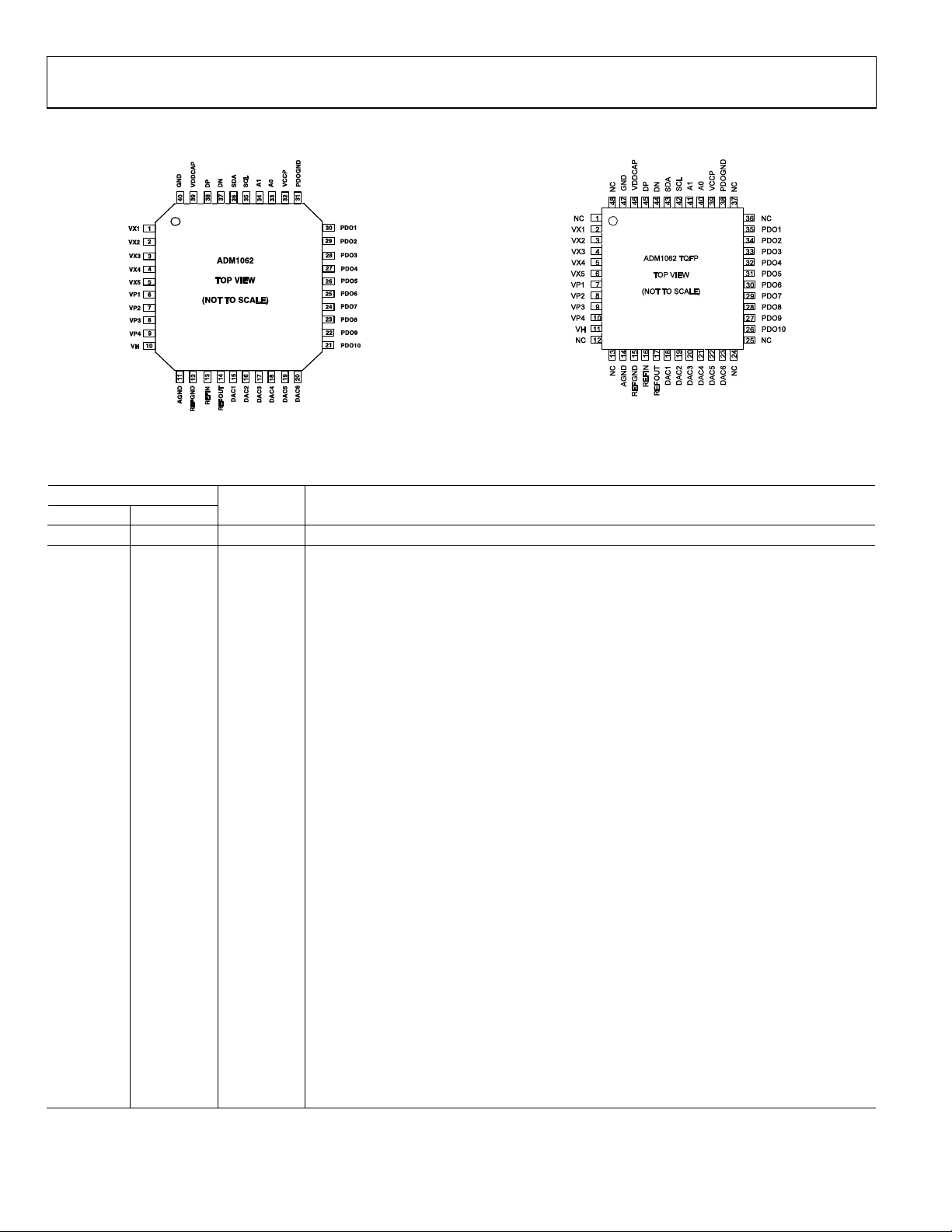
Figure 3. LFCSP Pin Configuration
Table 2. Pin Functional Descriptions
Pin Number
LFCSP TQFP
1 NC No connection.
1–5 2-6 VX1–5
6–9 7-10 VP1–4
10 11 VH
12-13 NC No connection.
11 14 AGND Ground return for input attenuators.
12 15 REFGND Ground return for on-chip reference circuits.
13 16 REFIN Reference input for ADC, nominally 2.048V.
14 17 REFOUT 2.048V reference output.
15–20 18-23 DAC1–6 Voltage output DACs. Default to high impedance at power-up.
24-25 NC No connection.
21–30 26-35 PDO10–1 Programmable output drivers.
36-37 NC No connection.
31 38 PDOGND Ground return for output drivers
32 39 VCCP
33 40 A0 Logic input which sets the 7th bit of the SMBus interface address.
34 41 A1 Logic input which sets the 6th bit of the SMBus interface address.
35 42 SCL SMBus clock pin. Open drain output requiring external resistive pull-up.
36 43 SDA SMBus data i/o pin. Open drain output requiring external resistive pull-up.
37 44 DN External Thermal Diode Cathode Connection
38 45 DP External Thermal Diode Anode Connection
39 46 VDDCAP
40 47 GND Supply ground.
48 NC No connection.
Mnemonic Description
High impedance inputs to supply fault detectors. Fault thresholds can be set at between
0.573V and 1.375V. Alternatively these pins can be used as general purpose digital inputs.
Low voltage inputs to supply fault detectors. Three input ranges can be set by altering the
input attenuation on a potential divider connected to these pins, the output of which connects
to a supply fault detector; these allow thresholds between 2.5V-6V, 1.25V-3V and 0.573V-
1.375V.
High voltage input to supply fault detectors. Three input ranges can be set by altering the
input attenuation on a potential divider connected to this pin, the output of which connects to
a supply fault detector; these allow thresholds between 6V-14.4V,2.5V-6V and 1.25V-3V.
Central charge pump voltage of 5.25V. A reservoir capacitor must be connected between this
pin and GND.
Device supply voltage. Linearly regulated from the highest of the VP1-4,VH pins and clamped
to a maximum of 4.75V
Figure 4. TQFP Pin Configuration
Rev. PrJ | Page 8 of 32

Preliminary Technical Data ADM1062
ABSOLUTE MAXIMUM RATINGS
Table 3.
Parameter Rating
Voltage on VH Pin 17 V
Voltage on VP Pins 7 V
Voltage on Any Other Input −0.3 V to +6.5 V
Input Current at any pin ±5 mA
Package Input Current ±20 mA
Maximum Junction Temperature (T
Storage Temperature Range −65°C to +150°C
Lead Temperature, Soldering
Vapor Phase, 60 s 215°C
ESD Rating all pins 2000 V
) 150°C
Jmax
ESD CAUTION
ESD (electrostatic discharge) sensitive device. Electrostatic charges as high as 4000 V readily accumulate on the
human body and test equipment and can discharge without detection. Although this product features
proprietary ESD protection circuitry, permanent damage may occur on devices subjected to high energy
electrostatic discharges. Therefore, proper ESD precautions are recommended to avoid performance
degradation or loss of functionality.
Stresses above those listed under Absolute Maximum Ratings
may cause permanent damage to the device. This is a stress
rating only; functional operation of the device at these or any
other conditions above those indicated in the operational
section of this specification is not implied. Exposure to absolute
maximum rating conditions for extended periods may affect
device reliability.
THERMAL CHARACTERISTICS
40-pin LFCSP Package:
= TBD°C/W
θ
JA
Rev. PrJ | Page 9 of 32

ADM1062 Preliminary Technical Data
TYPICAL PERFORMANCE CHARACTERISTICS
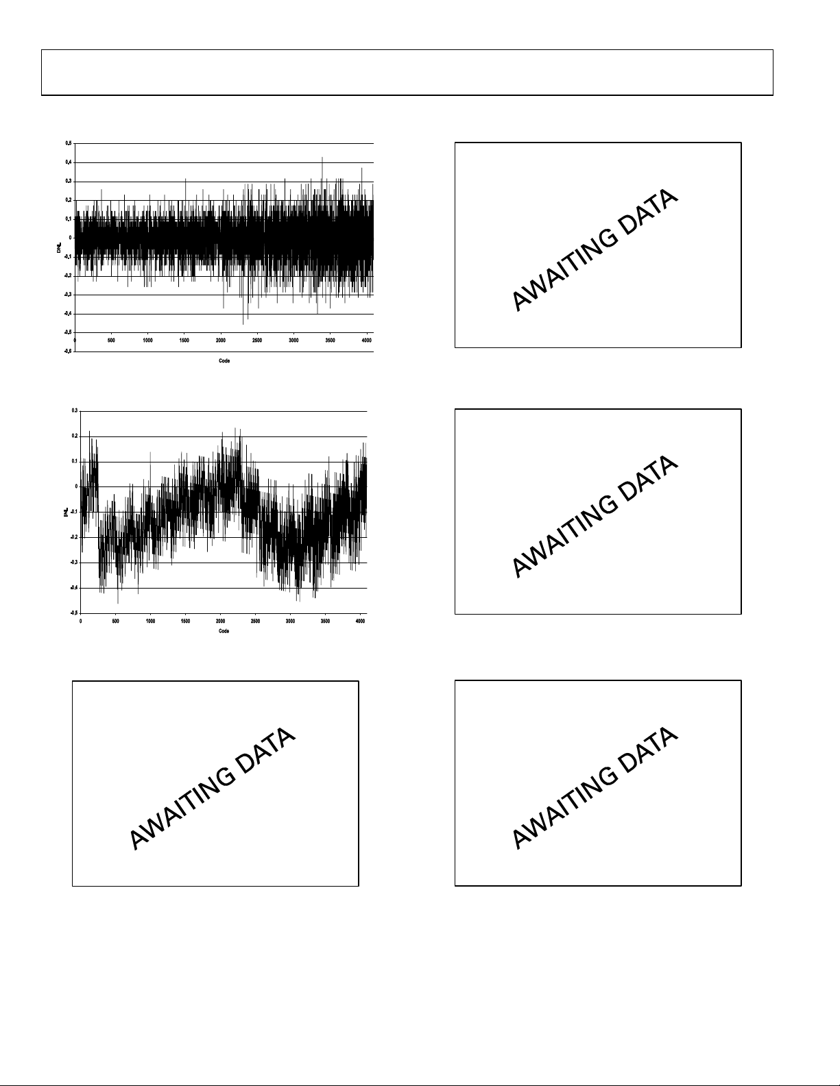
Figure 5. DNL for on- chip 12- bit ADC
Figure 6. INL for on- chip 12- bit ADC
Figure 8. IDD vs. VVP1 (Supply)
Figure 9. IVP1 vs. VVP1 (Not Supply)
Figure 7. VVDDCAP vs. VVH and VVP1
Rev. PrJ | Page 10 of 32
Figure 10. IDD vs. VVH
 Loading...