Analog Devices ADM1051 Datasheet

Precision Dual Voltage
a
FEATURES
Two Independent Controllers on One Chip
1.515 V and 1.818 V Outputs
Shutdown Inputs to Control Each Channel
Compatible with PC Motherboard TYPEDET Signal
ⴞ2.5% Accuracy Over, Line, Load, and Temperature
Low Quiescent Current
Low Shutdown Current
Works with External N-Channel MOSFETs for Low Cost
“Hiccup Mode” Fault Protection
No External Voltage or Current Setting Resistors
1.8 V/3.3 V ICH Sequenced Power-Up on ADM1051A
Small, 8-Lead SOIC Package
APPLICATIONS
Desktop Computers
Servers
Workstations
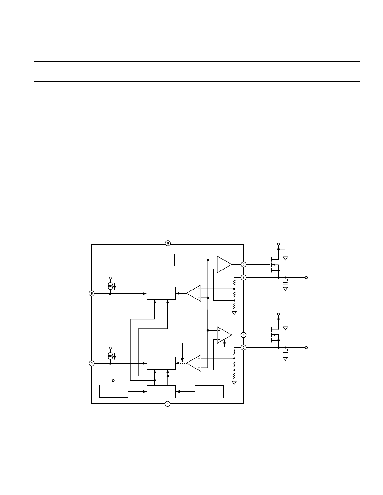
FUNCTIONAL BLOCK DIAGRAM
V
CC
ADM1051/ADM1051A
BANDGAP
REFERENCE
Regulator Controllers
ADM1051/ADM1051A
GENERAL DESCRIPTION
The ADM1051/ADM1051A are dual, precision, voltage regulator controllers intended for power rail generation and active bus
termination on personal computer motherboards. They contain a
precision 1.2 V bandgap reference and two channels consisting of
control amplifiers driving external power devices. Each channel
has a shutdown input to turn off amplifier output and Hiccup
Mode protection circuitry for the external power device. The
shutdown input on the 1.5 V channel can also be used with the
TYPEDET signal on a PC motherboard to select the output voltage.
The ADM1051/ADM1051A operate from a 12 V supply, which
gives sufficient headroom for the amplifiers to drive external
N-channel MOSFETs, operating as source-followers, as the
external series pass devices. This has the advantage that Nchannel devices are cheaper than P-channel devices of similar
performance, and the circuit is easier to stabilize than one using
P-channel devices in a common-source configuration.
V
IN
3.3V
CONTROL
AMPLIFIER
FORCE 1
100F
V
CC
SHDN1
SHDN2
50A
V
CC
50A
V
CC
POWER-ON
RESET
SHUTDOWN
CONTROL
NO CONNECTION
SHUTDOWN
CONTROL
CLK/DELAY
GENERATOR
GND
HICCUP
COMPARATOR
ON ADM1051A
HICCUP
COMPARATOR
REV. 0
Information furnished by Analog Devices is believed to be accurate and
reliable. However, no responsibility is assumed by Analog Devices for its
use, nor for any infringements of patents or other rights of third parties
which may result from its use. No license is granted by implication or
otherwise under any patent or patent rights of Analog Devices.
SENSE 1
2ⴛ100F
V
IN
3.3V
CONTROL
AMPLIFIER
FORCE 2
SENSE 2
CLOCK
OSCILLATOR
One Technology Way, P.O. Box 9106, Norwood, MA 02062-9106, U.S.A.
Tel: 781/329-4700 World Wide Web Site: http://www.analog.com
Fax: 781/326-8703 © Analog Devices, Inc., 2000
100F
2ⴛ100F
V
V
OUT1
OUT2

(VCC = 12 V ⴞ 6%, VIN = 3.3 V, TA = 0ⴗC to 70ⴗC, both
ADM1051/ADM1051A–SPECIFICATIONS
channels, unless otherwise noted. See Test Circuit.)
Parameter Min Typ Max Unit Test Conditions/Comments
OUTPUT VOLTAGE
Channel 1 1.515 V SHDN1 Floating
Channel 2 1.818 V
OUTPUT VOLTAGE ACCURACY –2.5 +2.5 % V
Load Regulation –5 +5 mV V
Line Regulation –5 +5 mV V
= 3.0 V to 3.6 V, I
IN
= 3.3 V, I
IN
= 3.0 V to 3.6 V, I
IN
= 10 mA to 1 A
OUT
5 VSB Supply Voltage Required for 4.6 V Test Circuit as Figure 7.2I
= 10 mA to 1 A
OUT
= 1 A
OUT
LOAD
Channel 2 Regulation
CONTROL AMPLIFIER
Control Amplifier Open-Loop Gain 100 dB
Control Amplifier Slew Rate 3 V/µs
Closed-Loop Settling Time 5 µsI
Turn-On Time 5 µs To 90% of Force High Output Level (C
Sense Input Impedance
Force Output Voltage Swing, V
1
(High) 10 V RL = 10 kΩ to GND
F
50 kΩ
Force Output Voltage Swing, VF (Low) 2 V RL = 10 kΩ to V
= 10 mA to 2 A
O
CC
HICCUP MODE
Hiccup Mode Hold-Off Time 30 60 90 ms See Figure 4
Hiccup Mode Threshold 0.8 × V
OUT
V
Hiccup Comparator Glitch Immunity 100 µs
Hiccup Mode On-Time 0.5 1.0 1.5 ms
Hiccup Mode Off-Time 20 40 60 ms
Power-On Reset Threshold 6 9 V
SHUTDOWN, SHDN1
Mode 1 (Shutdown) 0.8 V
Mode 2 (1.5 V Out) 2 3.9 V
Mode 3 (3.3 V Out) 4.3 5.3 V
Mode 4 (1.5 V Out) 6.2 12 V
SHUTDOWN, SHDN2
Shutdown Input Low Voltage, V
Shutdown Input High Voltage, V
IL
IH
2.0 V
0.8 V
Supply Current, Normal Operation 2.4 4.0 mA Shutdown Inputs Floating
Supply Current, Shutdown Mode 600 1000 µA Both Channels Shut Down
NOTES
1
Guaranteed by design.
2
5 VSB Supply is connected to, and measured at anode of Schottky Diode.
Specifications subject to change without notice.
1
1
= 500 mA
= 470 pF)
L
–2–
REV. 0

ADM1051/ADM1051A
WARNING!
ESD SENSITIVE DEVICE
ABSOLUTE MAXIMUM RATINGS*
(TA = 25°C unless otherwise noted)
VCC to GND . . . . . . . . . . . . . . . . . . . . . . . . . . . . . . . . . . 14 V
SHDN1, SHDN2 to GND . . . . . . . . –0.3 V to (V
+ 0.3 V)
CC
SENSE 1, SENSE 2 to GND . . . . . . . . . . . –0.3 V to +5.5 V
FORCE 1, FORCE 2 . . . . . . . Short-Circuit to GND or V
CC
Continuous Power Dissipation (TA = 70°C) . . . . . . . 650 mW
8-Lead SOIC (Derate 8.3 mW/°C Above 70°C)
Operating Temperature Range
Commercial (J Version) . . . . . . . . . . . . . . . . . . 0°C to 70°C
Storage Temperature Range . . . . . . . . . . . –65°C to +150°C
Lead Temperature (Soldering, 10 sec) . . . . . . . . . . . . 300°C
*This is a stress rating only; functional operation of the device at these or any other
conditions above those indicated in the operation sections of this specification is
not implied. Exposure to absolute maximum rating conditions for extended
periods of time may affect reliability.
THERMAL CHARACTERISTICS
8-Lead Small Outline Package:
θ
= 150°C/W
JA
ORDERING GUIDE
Temperature Package Package
Model Range Description Option
ADM1051JR 0°C to 70°C 8-Lead SOIC R-8
ADM1051AJR 0°C to 70°C 8-Lead SOIC R-8
PIN FUNCTION DESCRIPTIONS
Pin
No. Mnemonic Function
1 FORCE 2 Output of Channel 2 control amplifier
to gate of external N-channel MOSFET.
2 SENSE 2 Input from source of external MOSFET
to inverting input of Channel 2 control
amplifier, via output voltage-setting
feedback resistor network.
3 SHDN2 Digital Input. Active-low shutdown
control with 50 µA internal pull-up. The
output of Channel 2 control amplifier goes
to ground when SHDN2 is taken low.
4 GND Device Ground Pin.
5 SHDN1 Digital Input. Active-low shutdown con-
trol with 50 µA internal pull-up. See text for
more details of SHDN1 functionality.
6 SENSE 1 Input from source of external MOSFET to
inverting input of Channel 1 control amplifier, via output voltage-setting feedback
resistor network.
7 FORCE 1 Output of Channel 1 control amplifier to
gate of external N-channel MOSFET.
8V
CC
12 V Supply.
LEAVE OPEN OR
CONNECT TO
LOGIC SIGNALS
IF SHUTDOWN
REQUIRED
SHDN1
SHDN2
12V
V
CC
ADM1051/
ADM1051A
1F
FORCE 1
SENSE 1
FORCE 2
SENSE 2
PHD55N03LT
MTD3055VL
V
3.3V
V
3.3V
IN
IN
100F
2ⴛ100F
100F
2ⴛ100F
V
V
OUT1
OUT2
PIN CONFIGURATION
FORCE 2
SENSE 2
SHDN2
GND
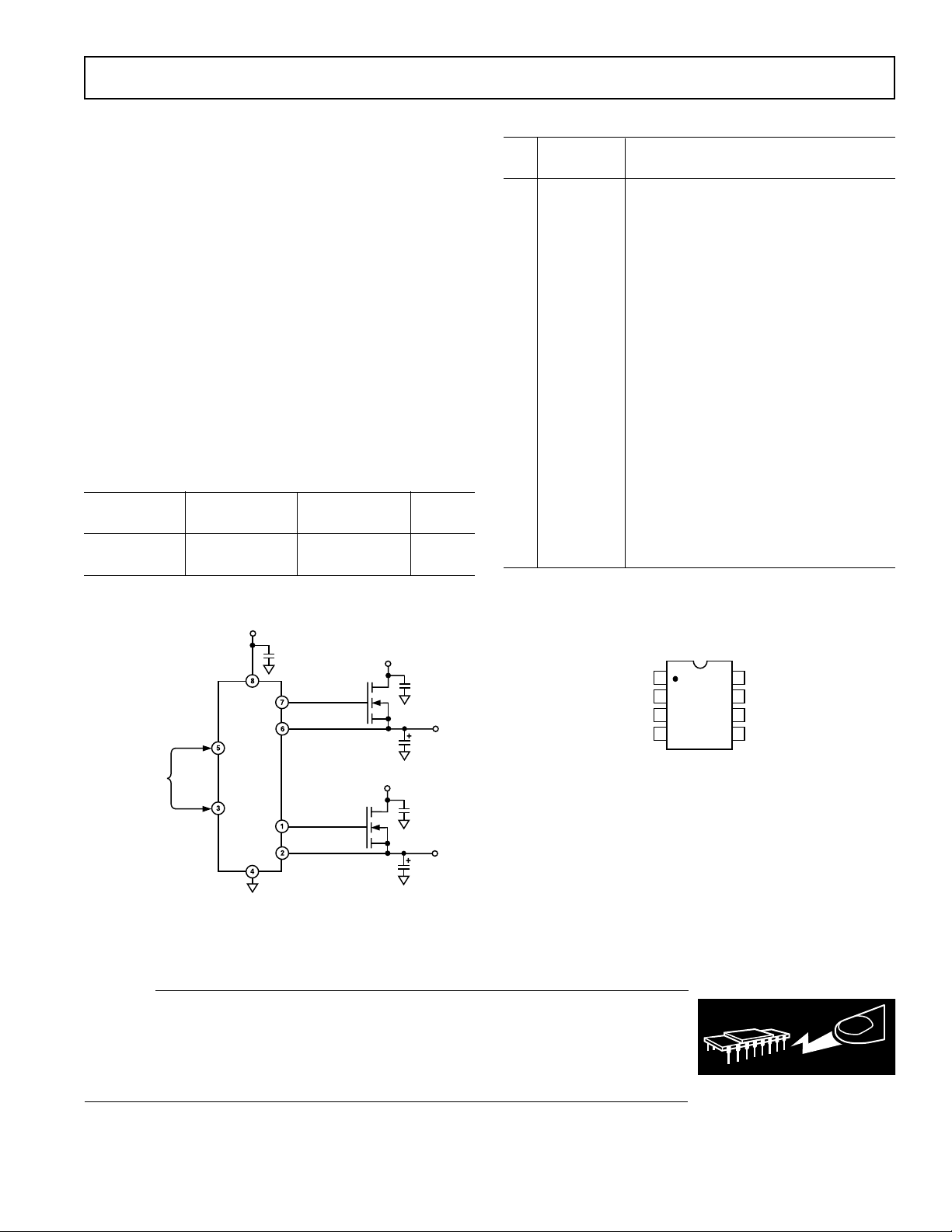
Figure 1. Test Circuit
CAUTION
ESD (electrostatic discharge) sensitive device. Electrostatic charges as high as 4000 V readily
accumulate on the human body a
nd test equipment and can discharge without detection.
Although the ADM1051/ADM1051A features proprietary ESD protection circuitry, permanent
damage may occur on devices subjected to high-energy electrostatic discharges. Therefore,
proper ESD precautions are recommended to avoid performance degradation or loss of
functionality.
1
2
ADM1051/
ADM1051A
3
TOP VIEW
(Not to Scale)
4
8
V
7
FORCE 1
6
SENSE 1
5
SHDN1
CC
REV. 0
–3–
 Loading...