

Page 1
Secondary-Side Controller with
FEATURES
Digital calibration via internal EEPROM
Supports SSI specification
Comprehensive fault detection
Reduced component count on secondary side
Standalone or microcontroller control
SECONDARY-SIDE FEATURES
Generates error signal for primary-side PWM
Output voltage adjustment and margining
Current sharing
Current-limit adjustment
OrFET control
Programmable soft-start slew rate
Standalone or microcontroller operation
Differential load voltage sense
AC mains undervoltage detection (ac sense)
Overvoltage protection
Current Share and Housekeeping
ADM1041A
INTERFACE AND INTERNAL FEATURES
SMBus interface (I2C-compatible)
Voltage-error amplifier
Differential current sense
Sense resistor or current transformer option
Overvoltage protection
Undervoltage protection
Overcurrent protection
Overtemperature protection
Start-up undervoltage blanking
Programmable digital debounce and delays
352-byte EEPROM available for field data
160-byte EEPROM for calibration
Ground continuity monitoring
APPLICATIONS
Network servers
Web servers
Power supply control
RS
V
OTP
DD
BIAS
THERMISTOR
PWM
CONTROLLER
V
DD
ISOLATION BARRIER
V
DD
V
DD
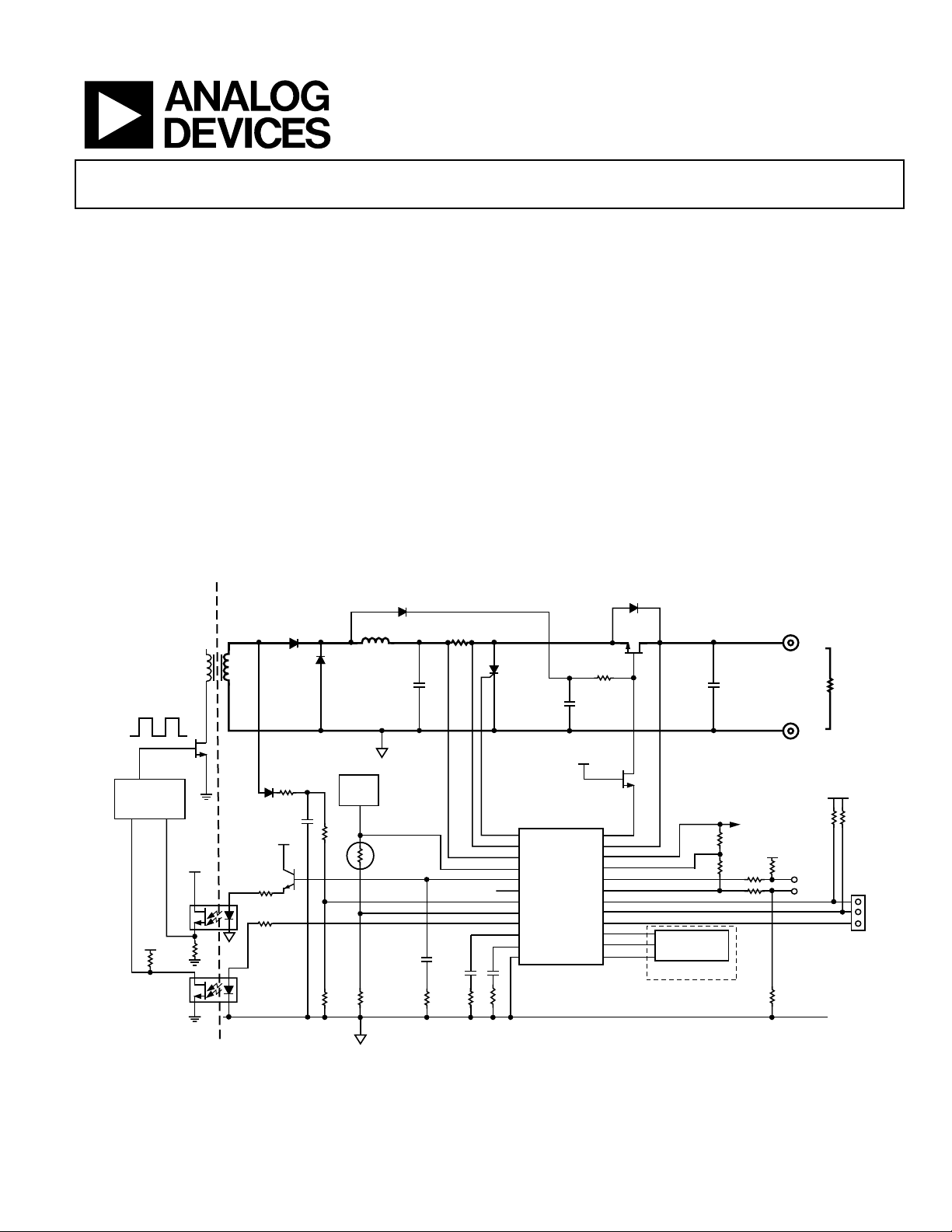
Figure 1. Typical Application Circuit
Rev. 0
Information furnished by Analog Devices is believed to be accurate and reliable.
However, no responsibility is assumed by Analog Devices for its use, nor for any
infringements of patents or other rights of third parties that may result from its use.
Specifications subject to change without notice. No license is granted by implication
or otherwise under any patent or patent rights of Analog Devices. Trademarks and
registered trademarks are the property of their respective owners.
OrFET
R
V
DD
ADM1041A
CBD
CS–/V
LS
C
+
S
V
DD
V
CMP
ICT
PULSE
AC_OK
DC_OK
MON2
PEN
C
CMP
SCMP
GND
SHRO
SHRS
V
V
PSON
ADD0
SCL
SDA
F
G
F
D
+
S
–
S
SHARE BUS
MICRO-
CONTROLLER
OPTIONAL
V
OUT
One Technology Way, P.O. Box 9106, Norwood, MA 02062-9106, U.S.A.
Tel: 781.329.4700 www.analog.com
Fax: 781.326.8703 © 2005 Analog Devices, Inc. All rights reserved.
V
OUT
LOAD
GND
VS+
V
S
V
DD
–
05405-001
Page 2

ADM1041A
TABLE OF CONTENTS
General Description ......................................................................... 3
I
Error Amplifier................................................................. 22
SHARE
Sample Application Circuit Description ................................... 3
Specifications..................................................................................... 6
Absolute Maximum Ratings.......................................................... 13
Thermal Characteristics ............................................................13
ESD Caution................................................................................ 13
Pin Configuration and Function Descriptions........................... 14
Terminology ................................................................................ 16
Theory of Operation ...................................................................... 18
Power Management.................................................................... 18
Gain Trimming and Configuration ......................................... 18
Differential Remote Sense Amplifier....................................... 19
Set Load Voltage ......................................................................... 19
Load Overvoltage (OV) ............................................................. 19
Local Voltage Sense .................................................................... 19
Local Overvoltage Protection (OVP) ...................................... 19
I
Clamp ................................................................................ 22
SHARE
SHARE_OK Detector ................................................................ 23
Pulse/AC
2............................................................................. 24
SENSE
Pulse ............................................................................................. 24
AC
.......................................................................................... 24
SENSE
OrFET Gate Drive...................................................................... 25
Oscillator and Timing Generators............................................... 27
Logic I/O and Monitor Pins...................................................... 27
SMBus Serial Port....................................................................... 30
Microprocessor Support............................................................ 30
Broadcasting................................................................................ 30
SMBus Serial Interface............................................................... 30
General SMBus Timing............................................................. 31
SMBus Protocols for RAM and EEPROM.............................. 33
SMBus Read Operations ........................................................... 35
Local Undervoltage Protection (UVP).................................... 19
False UV Clamp.......................................................................... 19
Voltage Error Amplifier............................................................. 20
Main Voltage Reference............................................................. 20
Current-Sense Amplifier ........................................................... 20
Current Sensing.......................................................................... 21
Current-Transformer Input ...................................................... 21
Current-Sense Calibration ........................................................ 21
Current-Limit Error Amplifier................................................. 21
Overcurrent Protection ............................................................. 22
Current Share.............................................................................. 22
Current-Share Offset.................................................................. 22
I
Drive Amplifier ................................................................ 22
SHARE
Differential Sense Amplifier ..................................................... 22
REVISION HISTORY
7/05—Revision 0: Initial Version
SMBus Alert Response Address (ARA) .................................. 36
Support for SMBus 1.1............................................................... 36
Layout Considerations............................................................... 36
Power-Up Auto-Configuration ................................................ 36
Extended SMBus Addressing.................................................... 37
Backdoor Access......................................................................... 37
Register Listing ............................................................................... 38
Detailed Register Descriptions ..................................................... 39
Manufacturing Data................................................................... 48
Microprocessor Support ................................................................ 49
Test Name Table.............................................................................. 51
Outline Dimensions....................................................................... 53
Ordering Guide .......................................................................... 53
Rev. 0 | Page 2 of 56
Page 3
ADM1041A
GENERAL DESCRIPTION
The ADM1041A is a secondary-side and management IC specifically designed to minimize external component counts and to
eliminate the need for manual calibration or adjustment on the
secondary-side controller. The principle application of this IC is
to provide voltage control, current share, and housekeeping
functions for single output in N+1 server power supplies.
The ADM1041A is manufactured with a 5 V CMOS process
and combines digital and analog circuitry. An internal
EEPROM provides added flexibility for trimming timing and
voltage and selecting various functions. Programming is done
via an SMBus serial port that also allows communication
capability with a microprocessor or microcontroller.
The usual configuration using this IC is on a one-per-output
voltage rail. Output from the IC can be wire-OR’ed together or
bused in parallel and read by a microprocessor. A key feature on
this IC is support for an OrFET circuit when higher efficiency
or power density is required.
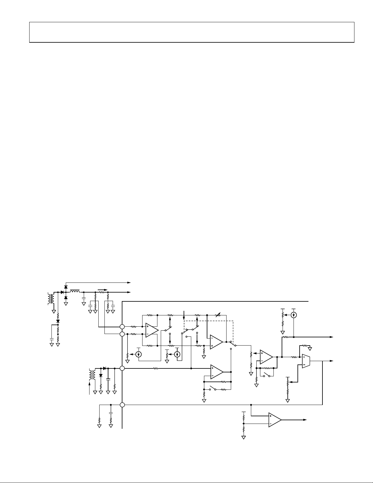
SAMPLE APPLICATION CIRCUIT DESCRIPTION
Figure 1 shows a sample application circuit using the
ADM1041A. The primary side is not detailed and the focus is
on the secondary side of the power supply.
The ADM1041A controls the output voltage from the power
supply to the designed programmed value. This programmed
value is determined during power supply design and is digitally
adjusted via the serial interface. Digital adjustment of the
current sense and current limit is also calibrated via the serial
interface, as are all of the internal timing specifications.
The control loop consists of a number of elements, notably the
inputs to the loop and the output of the loop. The ADM1041A
takes the loop inputs and determines what, if any, adjustments
are needed to maintain a stable output. To maintain a stable
loop, the ADM1041A uses three main inputs:
• Remote voltage sense
• Load current sense
• Current sharing information
In this example, a resistor divider senses the output current as a
voltage drop across a sense resistor (RS) and feeds a portion
into the ADM1041A. Remote local voltage sense is monitored
+ and VS− pins. Finally, current sharing information is fed
via V
S
back via the share bus. These three elements are summed
together to generate a control signal (V
loop via an optocoupler to the primary side PWM controller.
), which closes the
CMP
Another key feature of the ADM1041A is its control of an
OrFET. The OrFET causes lower power dissipation across the
OR'ing diode. The main function of the OrFET is to disconnect
the power supply from the load in the event of a fault occurring
during steady state operation, for example, if a filter capacitor or
rectifier fails and causes a short. This eliminates the risk of
bringing down the load voltage that is supplied by the redundant configuration of other power supplies. In the case of a
short, a reverse voltage is generated across the OrFET. This
reverse voltage is detected by the ADM1041A and the OrFET is
shut down via the F
pin. This intervention prevents any
G
interruption on the power supply bus. The ADM1041A can
then be interrogated via the serial interface to determine why
the power supply has shut down.
This application circuit also demonstrates how temperature can
be monitored within a power supply. A thermistor is connected
between the VDD and MON2 pins. The thermistor’s voltage
varies with temperature. The MON2 input can be programmed
to trip a flag at a voltage corresponding to an overheating power
supply. The resulting action may be to turn on an additional
cooling fan to help regulate the temperature within the power
supply.
PWM +
PRIMARY
DRIVER
OPTO-
COUPLER
AC PULSE
SENSE
ERROR
AMP
VOLT, TEMP MONITOR
AND FAULT DETECTION
ADM1041A
Figure 2. Application Block Diagram
DIFF CURRENT
SOFT
START
EEPROM AND
RAM AND TRIM
SENSE
SENSE
OrFET
CONTROL
CURRENT
SHARE
DIFF LOAD AND LOCAL
VOLTAGE SENSE
SMBus
LOAD
SHARE
BUS
(μC OR STANDALONE
OPERATION)
μC
R
Differences Between the ADM1041A and ADM1041
For all new designs, it is recommended to use the ADM1041A.
The parts differ as follows:
• The ADM1041 allows the internal VREF voltage reference to
be accessed at Pin 18. This is not accessible using the
ADM1041A.
• The ADM1041A has longer V
OK debounce and VDDOV
DD
debounce than the ADM1041.
• The GND_OK Disable bit (Register 11h) does not disable
when using the ADM1041. It does disable when using the
ADM1041A.
05405-002
Rev. 0 | Page 3 of 56
Page 4
ADM1041A
OUT
V
DRAINSOURCE
GATE
+ 10V
OUT
V = V
R1
R2
23
SHRS+
50kΩ
/SHRS–
S–
V
REMOTE
20
50kΩ
50kΩ
–VE SENSE
GAIN = (R1 + R2)/R2
50kΩ
50mV 50mV
SHARE BUS
1N4148
12V
DD
V
G
F
19
POLARITY
ORFET CONTROL
OrFET OK
REVERSEOK
ERROR
AMPLIFIER
SHARE
I
SCMP
22
SHARE
I
CLAMP
DRIVE
SHARE
I
SHRO
24
60μA
AMPLIFIER
SENSE
DIFFERENTIAL
CURRENT
REF
R
Q
CLK
1 mSec
R
V
AC SENSE
PENOK
LOADVOK
D
F
63
LS
/V
2
–/FS
S
C
+
S
C
PULSEOK
SQ
R
Q
CLK
1 Sec
REVERSE
VOLTAGE
DETECTOR
AC_OK
SQ
R
TO VOLTAGE ERROR AMP
DD
V
REF
V
,
SHARE
SHARE
OFFSET
(V
IOUT = 0)
CURRENT
REG 17h b7
9R
IRS/
R
SET
CURRENT
ICT
SHARE
ERROR AMP
CURRENT-LIMIT
V
SHAREOK
REF
LIMIT LEVEL
SET CURRENT-
CURRENT SHARE
SET GAIN
0.525V
1
SENSE
PULSE
AC
1.5V
SENSE
SELECT
AC
5.3kΩ
9
5.3kΩ
2
SENSE
AC
10
TRIM
HYSTERESIS
GAIN = 10
40kΩ
8
ICT
SENSE
CURRENT-
TRANSFORMER
CONFIGURATON
4
CMP
C
CURRENT
TRANSFORMER
CURRENT SENSE
05405-003
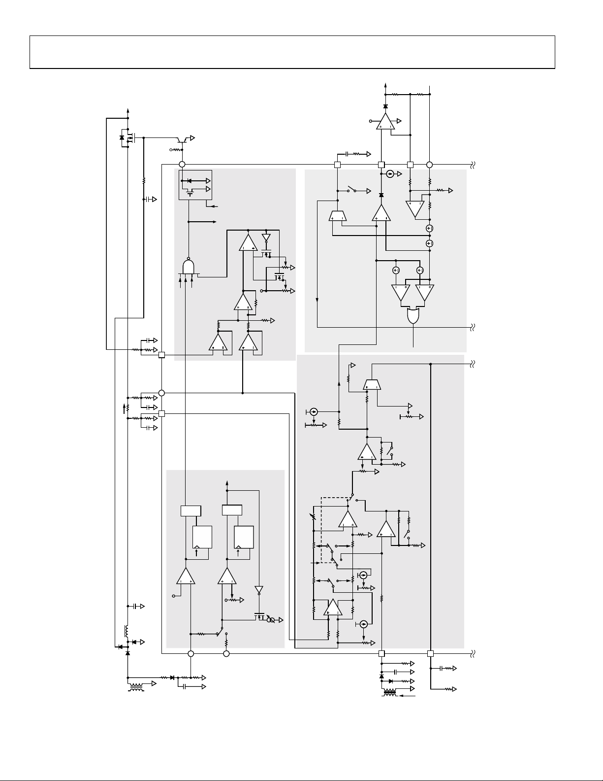
Figure 3. ADM1041A Diagram, Part 1
Rev. 0 | Page 4 of 56
Page 5
ADM1041A
LINK
CMP
V
5
VOLTAGE
ERROR AMP
OTP/
MON5
18
MON1
MON2
MON3
MON4
9
16
10
PSON
16
AC_OK
DC_OK
171718
CBD/ALERT
11
PEN
12
70μA
ON
SCL/
AC_OKLink
ADD0
SDA/
PS
151413
CS
SCL
PEN
SERIAL
INTERFACE
LINES
CONTROL
LOGIC AND GPIO
1V 3V
CURRENT LIMIT
DIFF. VOLTAGE SENSE
CURRENT SHARE CAPTURE
REF
1.5V
V
RAMP UP
SOFT-START
2.5V
VOLTAGE ERROR AMP
MON5
OCP
1.25V
AC_OK
OK
DD
V
DC_OK
OV
DD
V
CBD
CONFIGURE
CONTROL
REGISTERS
PWRON
STATUS
CONFIGURE
(READ
REGISTERS)
(WRITE
REGISTERS)
LOGIC
PENOK
MON4
AC_OK
ORFETOK
PSON
CLOCK
SHAREOK
RESET
MON1
MON2
MON3
GENERAL
OVP
UVP
I/Os
PEN
OCP
1.25V
AC_OK
PENOK
ORFETOK
SHAREOK
OCPF
OV
OK
DD
DD
V
V
LOADVOK
REF
V
1.25V
UVP
OVP
2.5V
1.25V
POWER MANAGEMENT
INTERNAL
REFERENCE
SET LOAD
OVERVOLTAGE
CLAMP
FALSE UV
1.5V
EXTREFOK
REFERENCE
MONITOR
INTREFOK
SQ
S
RQ
RQ
SET
LOAD
VOLTAGE
35kΩ
35kΩ
1.3
35kΩ
×
35kΩ
SET UV CLAMP
SET OVP
THRESHOLD
SET UVP
THRESHOLD
AUXILIARY
THRESHOLD
MAIN
BAND GAP
REFERENCE
POR
UVLLO
UVLHI
10μs–20μs
OVP
GNDOK
GROUND
MONITOR
gndok_dis
0.2V
21
+
S
V
REMOTE
FROM
SENSE
LOAD
20
–
S
V
2
LS
V
VOLTAGE SENSE
1
DD
V
ANALOG I/O PIN
HIGH VOLTAGE
NOTES:
1.
2.0V
6.0V–6.5V
XX
XX
ARE DIGITALLY
PROGRAMMBALE
STANDARD I/O PIN
2.
ALL POTENTIOMETERS ( )
3.
THROUGH REGISTERS
7
20
–
S
V
GND
05405-004
4.4V
4.0V
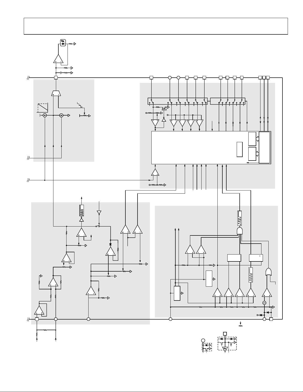
Figure 4. ADM1041A Diagram, Part 2
Rev. 0 | Page 5 of 56
Page 6

ADM1041A
SPECIFICATIONS
TA = –40 to +85°C, VDD = 5 V ± 10%, unless otherwise noted.
Table 1.
Parameter Min Typ Max Unit Test Conditions/Comments
SUPPLIES
VDD 4.5 5.0 5.5 V
IDD, Current Consumption 6 10 mA
Peak I
during EEPROM Erase Cycle
DD,
UNDERVOLTAGE LOCKOUT, VDD
1, 2
40 mA
Start-Up Threshold 4 4.3 4.5 V
Stop Threshold 3.7 4 4.2 V
Hysteresis 0.3 V
POWER BLOCK PROTECTION
VDD Overvoltage 5.8 6.2 6.5 V
VDD Overvoltage Debounce 300 500 700 μs Latching
Open Ground 0.1 0.2 0.35 V V
VDDOK Debounce 250 400 500 μs VDDOK
POWER-ON RESET
DC Level 1.5 2.2 2.75 V VDD rising
DIFFERENTIAL LOAD VOLTAGE SENSE INPUT,
−, VS+)
(V
S
VS− Input Voltage 0.5 V Voltage on Pin 20
VS+ Input Voltage VDD – 2 V Voltage on Pin 21
VS− Input Resistance 35 kΩ
VS+ Input Resistance 500 kΩ
V
Adjustment Range 1.7 to 2.3 V
NOM
Set Load Voltage Trim Step 0.10 to 0.14 % 1.7 V ≤ V
1.74 to 3.18 mV 8 bits, 255 steps
Reg 19h[7:0]. See Table 34
Set Load Overvoltage Trim Range 105 to 120 % 1.7 V ≤ V
Set Load Overvoltage Trim Step 0.09 % 8 bits, 255 step/s
1.6 mV Reg 08h[7:0]. See Table 17.
V
Recover from Load OV False to FG True 100 μs Reg 03h[1:0] = 00. See Table 12.
200 μs Reg 03h[1:0] = 01. See Table 12.
300 μs Reg 03h[1:0] = 10. See Table 12.
400 μs Reg 03h[1:0] = 11. See Table 12.
Operate Time from Load OV to FG False 2 μs
See Figure 9.
positive with respect to VS−
GND
See
Figure 6. V
= (VS+ – VS−); V
NOM
is typically 2 V
≤ 2.3 V typ
NOM
≤ 2.3 V min
NOM
+ = 2.24 V
S
NOM
Rev. 0 | Page 6 of 56
Page 7

ADM1041A
Parameter Min Typ Max Unit Test Conditions/Comments
LOCAL VOLTAGE SENSE, VLS,
See
AND FALSE UV CLAMP
Input Voltage Range3 2.3 (VDD – 2) V Set by external resistor divider.
Stage Gain 1.3 At VLS = 1.8 V
False UV Clamp, VLS, Input Voltage Nominal,
1.3 1.85 2.1 V
and Trim Range
Clamp Trim Step 0.2 % V
Clamp Trim Step 3.1 mV
Local Overvoltage 1.9 2.4 2.85 V
Nominal and Trim Range
OV Trim Step 0.15 % V
OV Trim Step 3.7 mV
Noise Filter, for OVP Function Only 5 25 μs
Local Undervoltage 1.3 1.7 2.1 V
Nominal and Trim Range
UV Trim Step 0.18 % V
UV Trim Step 3.1 mV
Noise Filter, for UVP Function Only 300 600 μs
VOLTAGE ERROR AMPLIFIER, V
Reference Voltage V
REF_SOFT_START
See Figure 15.
CMP
1.49 1.51 V TA = 25°C
Temperature Stability2 ±100 μV/°C −40°C ≤ TA ≤ 85°C
Long-Term Voltage Stability2 ±0.2 % Over 1,000 hr, TJ = 125°C
Soft-Start Period Range 0 40 ms Ramp is 7 bit, 127 steps
Set Soft-Start Period 300 μs Reg 10h[3:2] = 00. See Table 25.
10 ms Reg 10h[3:2] = 01. See Table 25.
20 ms Reg 10h[3:2] = 10. See Table 25.
40 ms Reg 10h[3:2] = 11. See Table 25.
Unity Gain Bandwidth, GBW 1 MHz See Figure 11.
Transconductance 1.9 2.7 3.5 mA/V At I
Source Current 250 μA At V
Sink Current 250 μA At V
DIFFERENTIAL CURRENT SENSE INPUT,
−, CS+
C
S
Reg 17h[7] = 0. See
Common-Mode Range 0 (VDD – 2) V Set by external divider
External Divider Tolerance Trim Range
−5 mV Reg 16h[5:3] = 000. See
(With Respect to Input)
−10 mV Reg 16h[5:3] = 001. See Table 31.
−20 mV Reg 16h[5:3] = 010. See Table 31.
5 mV Reg 16h[5:3] = 100. See Table 31.
10 mV Reg 16h[5:3] = 101. See Table 31.
20 mV Reg 16h[5:3] = 110. See Table 31.
External Divider Tolerance Trim Step Size 20 μV VCM = 2.0 V
(With Respect to Input) 39 μV 8 bits, 255 steps
78 μV Reg 14h[7:0]. See Table 29.
Figure 9.
RANGE
8 bits, 255 steps, Reg 18h[7:0].
Table 33.
See
RANGE
8 bits, 255 steps Reg 0Ah[7:0].
Table 19.
See
RANGE
8 bits, 255 steps, Reg 09h[7:0]. See
Table 18.
= ±180 μA
VCMP
> 1 V
VCMP
< VDD − 1 V
VCMP
Table 18.
I
mode. See Figure 13.
SENSE
Table 31.
Rev. 0 | Page 7 of 56
Page 8

ADM1041A
Parameter Min Typ Max Unit Test Conditions/Comments
DC Offset Trim Range (with Respect to Input) −8 mV Reg 17h[2:0] = 000. See Table 32 .
−15 mV Reg 17h[2:0] = 001. See Table 32.
−30 mV Reg 17h[2:0] = 010. See Table 32.
8 mV Reg 17h[2:0] = 100. See Table 32.
15 mV Reg 17h[2:0] = 101. See Table 32.
30 mV Reg 17h[2:0] = 110. See Table 32.
DC Offset Trim Step Size 30 μV VCM = 2.0 V, V
(with respect to input) 50 μV 8 bits, 255 steps
120 μV Reg 15h[7:0]. See Table 30.
CURRENT SENSE CALIBRATION
Total Current Sense Error2
(Gain and Offset)
= 2.0V, 0°C ≤ TA ≤ 85°C,
V
CSCM
SHRS = SHRO = 2 V. Gain = 230x.
±3 % Chopper on
±6 % Chopper off
Gain Range (I
) Max input voltage range at CS+, CS−
SENSE
Gain Setting 1 (Reg 16h[2:0] = 000) 65 V/V 34 mV – 44.5 mV. Gain = 65×.
Gain Setting 2 (Reg 16h[2:0] = 001) 85 V/V 26 mV – 34 mV. Gain = 85×.
Gain Setting 3 (Reg 16h[2:0] = 010) 110 V/V 20 mV – 26 mV. Gain = 110×.
Gain Setting 4 (Reg 16h[2:0] = 100) 135 V/V 16 mV – 20 mV. Gain = 135×.
Gain Setting 5 (Reg 16h[2:0] = 101) 175 V/V 12 mV – 16 mV. Gain = 175×.
Gain Setting 6 (Reg 16h[2:0] = 110) 230 V/V 9.5 mV – 12 mV. Gain = 230×
Full Scale (No Offset) 2.0 V VZO = 0
Attenuation Range 65 to 99 % Reg 06h[7:1]. See Table 15.
Current Share Trim Step (at SHRO) 0.4 % SHRS = SHRO = 1 V
8 mV 7 bits, 127 steps I
Gain Accuracy
Gain Accuracy
2, 4
, 40 mV at CS+, CS− −5 +5 %
2, 4
, 20 mV at CS+, CS− −5 ±1 +5 %
0 V ≤ V
CSCM
V
= input common mode.
CSCM
= 2.0 V, 0°C ≤ TA ≤ 85°C.
V
CSCM
Gain = 135×
Gain Accuracy
2, 4
, 40 mV at CS+, CS– −2.5 ±0.5 +2.5 %
= 2.0 V, 0°C ≤ TA ≤ 85°C.
V
CSCM
Gain = 65×
SHARE BUS OFFSET See Figure 13.
Current Share Offset Range 1.25 V
Reg 17h[7] = 1. See
Reg 17h[5] = 1. See
Zero Current Offset Trim Step 0 ≤ V
TRIM
0.4 % 8 bits, 255 steps, VCT = 1.0 V
5.5 mV Reg 05h[7:0]. See Table 14.
CURRENT TRANSFORMER SENSE INPUT, ICT
Reg 17h[7] = 1. See
Reg 06h = FEh. See
Gain Setting 0 4.5 V/V
Reg 17h[5] = 0, V
See Table 31
Gain Setting 1 2.57 V/V
Reg 17h[5] = 1. See
Reg 15h = 05h, approx 1 μA.
See Table 30. V
CT Input Sensitivity 0.45 0.5 0.68 V Gain setting = 4.5
CT Input Sensitivity 0.79 1.0 1.20 V Gain setting = 2.57
Input Impedance2 20 50 kΩ
Source Current 2.0 μA
Current-Transformer Input
See
Section.
Source Current Step Size 170 nA 15 steps Reg 15h[3:0]. See Table 30.
Reverse Current for Extended SMBus
Addressing (Source Current)
5
3.5 5 7 mA
Figure 38 and the Absolute
See
Maximum Ratings section.
= 0 V
DIFF
slope
SHARE
≤ 0.3 V. Gain = 65×.
Table 32.
Table 32.
≤ 1.25 V
Table 32.
Table 15.
= 2 V.
SHARE
Table 32.
= 2 V.
SHARE
Rev. 0 | Page 8 of 56
Page 9

ADM1041A
Parameter Min Typ Max Unit Test Conditions/Comments
CURRENT LIMIT ERROR AMPLIFIER See Figure 13
Current Limit Trim Range2 105 130 % After I
Current Limit Trim Step 1.1 %
Current Limit Trim Step 26.5 mV
2.0 ≤ V
Reg 04h[7:3]. See
Transconductance 100 200 300 μA/V I
Output Source Current 40 μA V
Output Sink Current 40 μA V
CCMP
CCMP
CCMP
CURRENT SHARE DRIVER See Figure 15
Output Voltage6 (VDD – 0.4) V RL = 1 kΩ, V
Short Circuit Source Current 55 mA
Source Current 15 mA
Current at which V
by more than 5%
Sink Current 60 100 μA V
CURRENT SHARE DIFFERENTIAL SENSE
See
SHARE
AMPLIFIER
VS– Input Voltage 0.5 V Voltage on Pin 20
V
Input Voltage VDD – 2 V Voltage on Pin 23
SHRS
Input Impedance2 65 100 kΩ V
SHRS
Gain 1.0 V/V
CURRENT SHARE ERROR AMPLIFIER
Transconductance, SHRS to SCMP 100 200 300 μA/V I
Output Source Current 40 μA V
Output Sink Current 40 μA V
SCMP
SCMP
SCMP
Input Offset Voltage 40 50 60 mV Master/slave arbitration
Share OK Window Comparator Threshold SHRS = 2 V ± SHR
(Share Drive Error) ±100 mV Reg 04h[1:0] = 00. See Table 13.
±200 mV Reg 04h[1:0] = 01. See Table 13.
±300 mV Reg 04h[1:0] = 10. See Table 13.
±400 mV Reg 04h[1:0] = 11. See Table 13.
CURRENT LIMIT Figure 10
Current Limit Control Lower Threshold 1.3 V V
CCMP
Current Limit Control Upper Threshold 3.5 V VS+ = 0 V, V
CURRENT SHARE CAPTURE V
SCMP
Current Share Capture Range 0.7 1 1.3 % Reg 10h[5:4] = 00. See Table 25.
1.4 2 2.6 % Reg 10h[5:4] = 01. See Table 25.
2.1 3 3.9 % Reg 10h[5:4] = 10. See Table 25.
2.8 4 5.2 % Reg 10h[5:4] = 11. See Table 25.
Capture Threshold 0.6 1.0 1.4 V
FET OR GATE DRIVE Open-drain N-channel FET
Output Low Level (On) 0.4 V IIO = 5 mA
0.8 V IIO = 10 mA
Output Leakage Current −5 +5 μA
REVERSE VOLTAGE COMPARATOR, FS, FD V
Common-Mode Range 0.25 2.0 (VDD – 2) V
CS−
Voltage set by C
Voltage on C
calibration
SHARE
≤ 2.8 V typ, 5 bits, 31 steps.
SHARE
Table 13.
= ±20 μA. See Figure 12.
= >1 V
= <VDD – 1 V
≤ VDD – 2 V
SHRS
does not drop
OUT
= 2.0 V
Figure 15
= 0.5 V, VS− = 0.5 V
= ±20 μA
> 1 V
< VDD – 1 V
THRESH
= 0.7 V, VS+ = 1.5 V
= 0 V
SCMP
= 3.5 V.
= FS
resistor divider.
S
− pin, TA = 25°C.
S
Rev. 0 | Page 9 of 56
Page 10

ADM1041A
Parameter Min Typ Max Unit Test Conditions/Comments
Reverse Voltage Detector Turn-Off Threshold VCS− = 2 V for threshold specs
100 mV Reg 03h[7:6] = 00. See Table 12.
150 mV Reg 03h[7:6] = 01. See Table 12.
200 mV Reg 03h[7:6] = 10. See Table 12.
250 mV Reg 03h[7:6] = 11. See Table 12.
Reverse Voltage Detector Turn-On Threshold VCS− = 2 V for threshold specs
20 mV Reg 03h[5:4] = 00. See Table 12.
30 mV Reg 03h[5:4] = 01. See Table 12.
40 mV Reg 03h[5:4] = 10. See Table 12.
50 mV Reg 03h[5:4] = 11. See Table 12.
FD Input Impedance 500 kΩ
FS Input Impedance 20 kΩ
AC
1/AC
SENSE
AC or Bulk Sense
Threshold Voltage 1.25 V
Threshold Adjust Range 1.10 1.40 V
Threshold Trim Step 0.8 % 1.10 ≤ V
10 mV
Hysteresis Adjust Range 200−550 mV V
Hysteresis Trim Step 50 mV
Noise Filter 0.6 1 1.2 ms
PULSE-IN
Threshold Voltage 0.525 V
PULSE_OK On Delay 1 μs
PULSE_OK Off Delay 0.8 1 1.2 s
OSCILLATOR −5 +5 % Unless otherwise specified
OCP
OCP Threshold Voltage2 0.3 0.5 0.7 V Force C
Reg 11h[2] = 0. See Table 26.
OCP Shutdown Delay Time (Continuous
Period in Current Limit)
2 s Reg 12h[4:3] = 01. See Table 27.
3 s Reg 12h[4:3] = 10. See Table 27.
4 s Reg 12h[4:3] = 11. See Table 27.
OCP Fast Shutdown Delay Time 0 100 ms
MON1, MON2, MON3, MON4
Sense Voltage 1.21 1.25 1.29 V
Hysteresis 0.1 V
OVP Noise Filter 5 25 μs
UVP Noise Filter 300 600 μs
OTP (MON5) Reg 0Fh[4:2] = 01x or 10x. See Table 24.
Sense Voltage Range 2.2 2.45 V
OTP Trim Step 24 mV 2.1 ≤ V
Hysteresis 100 130 160 μA V
2 COMPARATOR
SENSE
1 s Reg 12h[4:3] = 00. See
Reg 12h[2] = 0
Reg 0Dh[3:2] = 00. See
Table 22 .
Reg 12h[2] = 1
Reg 0Eh[7:6] = 00. See
Table 23.
Min: DAC = 0
Max: DAC = Full Scale
≤ 1.4 V
TRIM
5 bits, 31 steps
Reg 0Ch[7:3]. See
> 1 V, R
ACSENSE
200 ≤ V
TRIM
Reg 0Ch[2:0]. See
CMP
Table 21.
= 909R
THEVENIN
≤ 550 mV. 7 steps
Table 21.
for drop in V
CMP
Table 27.
Reg 11h[2] = 1. See
= 1.5 V
VC
CMP
≤ 2.45 V
TRIM
Table 26.
4 bits, 15 steps, Reg 0Bh[7:4].
Table 20.
See
= 2 V
OTP
Rev. 0 | Page 10 of 56
Page 11

ADM1041A
Parameter Min Typ Max Unit Test Conditions/Comments
OVP Noise Filter 5 25 μs
UVP Noise Filter 300 600 μs
PSON7 Reg 0Eh[4:2] = 00x. See Table 23.
Input Low Level8 0.8 V
Input High Level8 2.0 V
Debounce 80 ms Reg 0Fh[1:0] = 00. See Table 24.
0 ms Reg 0Fh[1:0] = 01. See Table 24.
40 ms Reg 0Fh[1:0] = 10. See Table 24.
160 ms Reg 0Fh[1:0] = 11. See Table 24.
PEN7, DC_OK7, CBD, AC_OK
Open-Drain N-Channel Option
Output Low Level = On8 0.4 V I
Open-Drain P-Channel V
Output High Level = On8 2.4 V I
Leakage Current −5 +5 μA
DC_OK7 Reg 0Fh[7:5] = 00x. See Table 24.
DC_OK, On Delay (Power-On and OK Delay) 400 ms Reg 0Eh[1:0] = 00. See Table 23.
200 ms Reg 0Eh[1:0] = 01. See Table 23.
800 ms Reg 0Eh[1:0] = 10. See Table 23.
1600 ms Reg 0Eh[1:0] = 11. See Table 23.
DC_OK, Off Delay (Power-Off Early Warning) 2 ms Reg 10h[7:6] = 00. See Table 25.
0 ms Reg 10h[7:6] = 01. See Table 25.
1 ms Reg 10h[7:6] = 10. See Table 25.
4 ms Reg 10h[7:6] = 11. See Table 25.
SMBus, SDL/SCL
Input Voltage Low8 0.8 V
Input Voltage High8 2.2 V
Output Voltage Low8 0.4 V VDD = 5 V, I
Pull-Up Current 100 350 μA
Leakage Current −5 +5 μA
ADD0, HARDWIRED ADDRESS BIT
ADD0 Low Level8 0.4 V
ADD0 Floating VDD/2 V Floating
ADD0 High8 VDD − 0.5 V
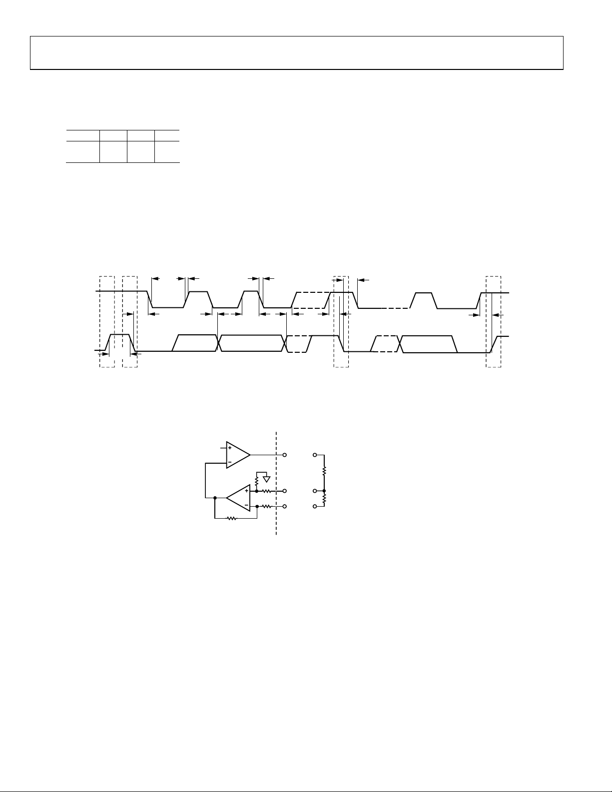
SERIAL BUS TIMING See Figure 5
Clock Frequency 400 kHz
Glitch Immunity, tSW 50 ns
Bus Free Time, t
Start Setup Time, t
Start Hold Time, t
SCL Low Time, t
SCL High Time, t
4.7 μs
BUF
4.7 μs
SU;STA
4 μs
HD;STA
4.7 μs
LOW
4 μs
HIGH
SCL, SDA Rise Time, tR 1000 ns
SCL, SDA Fall Time, tF 300 ns
Data Setup Time, t
Data Hold Time, t
250 ns
SU;DAT
300 ns
HD;DAT
EEPROM RELIABILITY
Endurance9 100 250 k cycles
Data Retention10 100 Years
Reg 0Fh[4:2] = 010 or 100.
Table 24.
See
Reg 0Fh[4:2] = 011 or 101.
See Table 24.
= 4 mA
SINK
OH_PEN
= 4 mA
SOURCE
= 4 mA
SINK
Rev. 0 | Page 11 of 56
Page 12
ADM1041A
A
1
This specification is a measure of IDD during an EEPROM page erase cycle. The current is a dynamic. Refer to Figure 29 for a typical IDD plot during an EEPROM page
erase.
2
This specification is not production tested, but is supported by characterization data at initial product release.
3
Four external divider resistors are the same ratio, which is selected to produce 2.0 V nominal at Pin 21 while at zero load current. Recommended values are
R
R
4
Chopper off.
5
The maximum specification here is the maximum source current of Pin 8 as specified by the Absolute Maximum Ratings.
6
All internal amplifiers accept inputs with common range from GND to VDD − 2 V. The output is rail-to-rail, but the input is limited to GND to VDD − 2 V. See Figure 6.
7
These pins can be configured as open-drain N-channel or P-channel, (except PSON) and as normal or inverted logic polarity.
8
A logic true or false is defined strictly according to the signal name. Low and high refer to the pin or signal voltages.
9
Endurance is qualified to 100,000 cycles as per JEDEC Std. 22, Method A117, and measured at −40°C, +25°C, and +85°C. Typical endurance at +25°C is 250,000 cycles.
10
Retention lifetime equivalent at junction temperature (TJ) = 55°C as per JEDEC Std. 22, Method A117. Retention lifetime based on an activation energy of 0.6 V.
3.3 V 5.0 V 12 V
680R 1K.5 5K1
TOP
1K 1K 1K
BOTTOM
Derates with junction temperature.
SCL
SD
t
t
BUF
PS
HD:STA
t
LOW
t
R
t
HD:DAT
t
F
t
HIGH
t
SU:DAT
S
Figure 5. Serial Bus Timing Diagram
t
SU:STA
t
HD:STA
t
SU:STO
P
05405-005
SHRO
SHRS+
SHRS–
VA = V
R1
VBVAVB = V
R1
R1 + R2 ≥ 1kΩ
Figure 6. Amplifier Inputs and Outputs
DD
DD
– 0.4V
–2V
05405-006
Rev. 0 | Page 12 of 56
Page 13

ADM1041A
ABSOLUTE MAXIMUM RATINGS
Table 2.
Parameter Rating
Supply Voltage (Continuous), VDD 6.5 V
Data Pins SDA, SCL, V
DATA
+ 0.5 V,
V
DD
GND − 0.3 V
Continuous Power at 25°C, P
Operating Temperature, T
AMB
450 mW
D-QSOP24
−40°C to +85°C
Junction Temperature, TJ 150°C
Storage Temperature, T
Lead Temperature
(Soldering, 10 Seconds), T
ESD Protection on All Pins, V
−60°C to +150°C
STG
300°C
L
2 kV
ESD
Thermal Resistance, Junction to Air, θJA 150°C/W
ICT Source Current1 7 mA
1
This is the maximum current that can be sourced out from Pin 8 (ICT pin).
ESD CAUTION
ESD (electrostatic discharge) sensitive device. Electrostatic charges as high as 4000 V readily accumulate on
the human body and test equipment and can discharge without detection. Although this product features
proprietary ESD protection circuitry, permanent damage may occur on devices subjected to high energy
electrostatic discharges. Therefore, proper ESD precautions are recommended to avoid performance
degradation or loss of functionality.
Stresses above those listed under Absolute Maximum Ratings
may cause permanent damage to the device. This is a stress
rating only; functional operation of the device at these or any
other conditions above those indicated in the operational
section of this specification is not implied. Exposure to absolute
maximum rating conditions for extended periods may affect
device reliability.
THERMAL CHARACTERISTICS
24-lead QSOP: θJA = 150°C/W
Rev. 0 | Page 13 of 56
Page 14
ADM1041A
PIN CONFIGURATION AND FUNCTION DESCRIPTIONS
PULSE/AC
AC
VLS/CS–/FS
1/MON1
SENSE
2/MON2
SENSE
CBD/ALERT
C
V
GND
PEN
V
DD
CS+
CMP
CMP
F
ICT
1
2
3
4
5
6
D
7
8
9
10
11
12
ADM1041A
TOP VIEW
(Not to Scale)
SHRO
24
23
SHRS+
22
SCMP
21
V
+
S
20
V
–/SHRS–
S
19
F
G
18
AC_OK/OTP/MON5
17
DC_OK/MON4
16
PSON/MON3
ADD0
15
SDA/PS
14
13
ON
SCL/AC_OKLink
LINK
05405-007
Figure 7. Pin Configuration
Table 3. Pin Function Descriptions
Pin No. Mnemonic Description
1 VDD Positive Supply for the ADM1041A. Normal range is 4.5 V to 5.5 V. Absolute maximum rating is 6.5 V.
2 VLS/CS–/FS
Inverting Differential Current Sense Input, Local Voltage Sense Pin, and OrFET Source. These three functions
are served by a common divider. The local voltage sense input is used for local overvoltage and undervoltage
sensing. This pin also provides an input to the false UV clamp that prevents shutdown during an external load
overvoltage condition. When supporting an OrFET circuit, this pin represents the FET source and is the
inverting input of a differential amplifier looking for the presence of a reverse voltage across the FET, which
might indicate a failure mode.
3 CS+
Noninverting Differential Current Sense Input. The differential sensitivity of C
+ and CS– is normally around 10
S
mV to 40 mV at the input to the ADM1041A. Nulling any external divider offset is achieved by injecting a
trimmable amount of current into either the inverting or noninverting input of the second stage of the
current sense amplifier. A compensation circuit is used to ensure the amount of current for zero-offset tracks
the common-mode voltage. Nulling of any amplifier offset is done in a similar manner except that it does not
track the common-mode voltage.
4 C
CMP
Current Error Amplifier Compensation. This pin is the output of the current limit transconductance error
amplifier. A series resistor and a capacitor to ground are required for loop compensation.
5 V
CMP
Voltage Error Amplifier Compensation. This is the output of a voltage error transconductance amplifier.
Compensate with a series capacitor and resistor to ground. An external emitter-follower or buffer is typically
used to drive an optocoupler. Output voltage positioning may be obtained by placing a second resistor
directly to ground. Refer to Analog Devices applications notes on voltage positioning.
6 FD
A divider from the OrFET drain is connected here. A differential amplifier is then used to detect the presence
of a reverse voltage across the FET, which indicates a fault condition and causes the OrFET gate to be pulled
low.
7 GND
Ground. This pin is double bonded for extra reliability. If the ground pin goes positive with respect to the
remote sense return (V
–) for a sustained period indicating that the negative remote sense line is
S
disconnected, PEN is disabled.
8 ICT
Input for Current Transformer. The sensitivity of this pin is suitable for the typical 0.5 V to 1 V signal that is
normally available. If this function is enabled, the C
+ amplifier is disabled. This pin is also used for extended
S
SMBus addressing, that is, pulled below ground to allow additional SMBus addresses.
9
PULSE/AC
MON1
SENSE
Pulse Present, AC/Bulk Sense 1, or Monitor 1 Input.
1/
PULSE: This tells the OrFET circuit that the voltage from the power transformer is normal. A peak hold allows
the OrFET circuit to pass through the pulse skipping that occurs with very light loads, but turns off the circuit
about one second after the last pulse is recognized.
1: This sense function also uses the peak voltage on this pin to measure the bulk capacitor voltage. If
AC
SENSE
too low, AC_OK and DC_OK can warn of an imminent loss of power. Threshold level and hysteresis can be
trimmed. When not selected, AC
1 defaults to true.
SENSE
MON1: When MON1 is selected for this pin, its input is compared against a 1.25 V comparator that could be
used for monitoring a postregulated output; includes overvoltage, undervoltage, and overtemperature
conditions.
Rev. 0 | Page 14 of 56
Page 15

ADM1041A
Pin No. Mnemonic Description
10 AC
11 CBD/ALERT
12 PEN
13 SCL/AC_OKLink SCL: SMBus Serial Clock Input.
14 SDA/PSONLINK SDA: SMBus Serial Data Input and Output.
15 ADD0
16 PSON/MON3
17 DC_OK/MON4
18
19 FG
20 VS–/SHRS–
21 VS+
22 SCMP
2/MON2 AC/Bulk Sense Input 2 or Monitor 2 Input.
SENSE
AC
2: This alternative AC
SENSE
for the OrFET. It also allows dc and optocoupled signals that are not suitable for the OrFET control.
MON2: When MON2 is selected for this pin, its input is compared against a 1.25 V comparator that could be
used for monitoring a postregulated output; includes overvoltage, undervoltage, and overtemperature
conditions.
CBD: The crowbar drive pin allows implementation of a fast shutdown in case of a load overvoltage fault. The
pin can be configured as an open-drain N-channel or P-channel and is suitable for driving a sensitive gate SCR
crowbar. An external transistor is required if a high gate current is needed. Either polarity may be selected.
ALERT: This pin can be configured to provide an ALERT function in microprocessor-supported applications
where any of several ICs in a redundant system that detects a problem can interrupt and shut down the
power supply. An alternative use is as a general-purpose logic output signal.
Power Enable. This pin can be configured as an open-drain N-channel or P-channel that typically drives the
PEN optocoupler. Providing that the PSON pin has been asserted to turn the output on, and that there are no
faults, this pin drives an optocoupler on enabling the primary PWM circuit. Either polarity may be selected.
AC_OKLink: In nonmicroprocessor applications, this pin can be programmed to give the status of AC
the ICs on the same bus. The main effect is to turn on undervoltage blanking whenever the sense circuit
monitoring ac or bulk dc detects a low voltage.
PSONLINK: In non-microprocessor applications, this pin can be programmed to provide the PSON status to
other ICs. This allows just one IC to be the PSON interface to the host system, or the PS
PSON interface.
Chip Address Pin. There are three addresses possible using this pin, which are achieved by tying ADD0 to
ground, tying to V
, or being left to float. One address bit is available via programming at the
DD
device/daughter card level, so the total number of addressable ICs can be increased to six.
PSON: In nonmicroprocessor configurations, this is power supply on. As a standard I/O, this pin is rugged
enough for direct interface with a customer’s system. Either polarity may be selected.
MON3: When MON3 is selected for this pin, its input is compared against a 1.25 V comparator that could be
used for monitoring a postregulated output; includes overvoltage, undervoltage, and overtemperature
conditions.
DC_OK: This pin is the output of a general-purpose digital I/O that can be configured as open-drain
N-channel or open-drain P-channel suitable for wire-OR'ing with other ICs and direct interfacing with a
customer’s system. Either polarity may be selected.
MON4: When MON4 is selected for this pin, its input is compared against a 1.25 V comparator that could be
used for overtemperature protection and for monitoring a postregulated output; includes overvoltage,
undervoltage, and overtemperature conditions.
AC_OK/OTP/
MON5
Buffered Output, Overtemperature Protection, or Monitor 5.
AC_OK: This option can be configured as N-channel or P-channel and as normal or inverted polarity. At
system level, a true AC_OK is used to indicate that the primary bulk voltage is high enough to support the
system and, when false, that dc output is about to fail.
MON5: A further option is to configure this as an analog input, MON5, with a flexible hysteresis and
trimmable 2.5 V reference. This makes the pin particularly suitable for overtemperature protection (OTP)
sensing. Since hysteresis uses a switched 100 μA current source, hysteresis can be adjusted via the source
impedance of the external circuit. It can also be used for OVP and UVP functions.
FET Gate Enable. When supporting an OrFET circuit, this is the gate drive pin. Because the open-drain voltage
on the chip is limited to V
DD
the OrFET. This pin is configured as an open-drain N-channel. Either output polarity, low = on or low = off,
may be selected.
This pin is used as the ground input reference for the current share and load voltage sense circuits. It should
be tied to ground at the common remote sense location. The input impedance is about 35 kΩ to ground.
This pin is the positive remote load voltage sense input and is normally divided down from the power supply
output voltage to 2.0 V at no-load using an external voltage divider. The input impedance is high.
Output of the Current Share Transconductance Error Amplifier. Compensation is a series capacitor and
resistor to ground. While V
DD
enabled (PEN true) and the clamp is released, the compensation capacitor charges, providing a slow walk-in.
The error amplifier input has a built-in bias so that all slaves in a parallel supply system do not compete with
the master for control of the share bus.
input can be used when the AC
SENSE
source must be different from that used
SENSE
LINK itself can be the
ON
SENSE
to all
, an external level shifter is required to drive the higher gate voltages suitable for
is normal and PEN is false, this pin is clamped to ground. When the converter is
Rev. 0 | Page 15 of 56
Page 16

ADM1041A
Pin No. Mnemonic Description
23 SHRS+
24 SHRO
Table 4. Default Pin States During EEPROM Download
Pin No. Mnemonic State
11 CBD High impedance (Hi-Z) at power-up and until the end of the EEPROM download (approximately 20 ms).
12 PEN High impedance (Hi-Z) at power-up and until the end of the EEPROM download (approximately 20 ms).
17 DC_OK Active low (low if DC_OK true) at power-up. This pin is reconfigured during the EEPROM download.
18 AC_OK Active low (low if DC_OK true) at power-up. This pin is reconfigured during the EEPROM download.
19 FG High impedance (Hi-Z) at power-up and until the end of the EEPROM download (approximately 20 ms).
Current Share Sense. This is the noninverting input of a differential sense amplifier looking at the voltage on
the share bus. For testing purposes, this pin is normally connected to SHRO. Calibration always expects this
pin to be at 2.0 V with respect to SHRS–/V
or an additional gain stage, must be used.
Current Share Output. This output is capable of driving the share bus of several power supplies between 0 V
– 0.4 V (10 kΩ bus pull-down in each supply). Where a higher share bus voltage is required, an
and V
DD
external amplifier is necessary. The current share output from the supply, when bused with the share output
of other power supplies working in parallel, allows each of the supplies to contribute essentially equal
currents to the load.
This pin is reconfigured at the end of the EEPROM download.
This pin is reconfigured at the end of the EEPROM download.
This pin is reconfigured at the end of the EEPROM download.
–. If a higher share voltage is required, a resistor divider from SHRO
S
TERMINOLOGY
Table 5.
Mnemonic Description
POR
UVL
CVMode
CCMode
UVP
OVP
OCP
OTP
UVB
Power-On Reset. When VDD is initially applied to the ADM1041A, the POR function clears all latches and puts
the logic into a state that allows a clean start-up.
Undervoltage Lockout. This is used on VDD to prevent spurious modes of operation that might occur if VDD
is below a specific voltage.
Constant Voltage Mode. This is the normal mode of operation of the power supply main output. The output
voltage remains constant over the whole range of current specified.
Constant Current Mode. This mode of operation occurs when the output is overloaded until or unless a
shutdown event is triggered. The output current control level remains constant down to 0 V.
Undervoltage Protection. If the output being monitored is detected as going under voltage, the UVP function
sends a fault signal. After a delay, PEN goes false, the output is disabled, and either latch-off or an autorestart
occurs, depending on the mode selected. The DC_OK output also goes false immediately to show that the
output is out of tolerance.
Overvoltage Protection. If the output being monitored is detected as going over voltage, the OVP function
latches and sends a fault signal, PEN goes false, and CBD goes true. The DC_OK output also goes false
immediately. OVP faults are always latching and require the cycling of PSON or VDD or SMBus command to
reset the latch.
Overcurrent Protection. If the output being monitored is detected as going over current for a certain time,
the OCP function sends out a fault signal that triggers a shutdown that can be latched or allowed to
autorestart, depending on the mode selected. Prior to shutting down, the DC_OK output goes false warning
the system that output is going to be lost. The latch is the same one used for OVP. For autorestart, the OCP
timeout period is configurable.
Overtemperature Protection. If the temperature being sensed is detected as going over the selected limit, the
OTP function sends out a fault signal that triggers a shutdown that can be latched or allowed to auto-restart
depending on the mode selected. Prior to shutting down, the DC_OK output goes false warning the system
that output is going to be lost. The latch is the same one used for OVP.
Undervoltage Blanking. The UVP function is blanked (disabled) during power-up or if the ACSENSE function is
false (ac line voltage is low). When in constant current mode, UVB is disabled. The status of ACSENSE must be
known to the IC, either by virtue of the on-board ACSENSE or communicated by the SMBus with the help of
an external microprocessor or by using AC_OKLink. When in constant-current mode, due to an overload, UVB
is applied for the overcurrent ride-through period.
Rev. 0 | Page 16 of 56
Page 17

ADM1041A
Mnemonic Description
DC_OK
AC_OK
DC_OK on delay The DC_OK output is kept false for typically 100 ms to 900 ms during power-up.
DC_OK off delay
Debounce Digital Noise
Filter
ACSENSE1
Pulse OK
AC Hysteresis
ACSENSE2
Soft-Start
VDD–OVP
VDD–UVL
Auto Restart Mode
VREF–MON
GND–MON
The DC_OK function advises the system on the status of the power supply. When it is false, the system is
assured of at least 1 ms of operation if ac power is lost for any reason. Other turn-off modes provide more
warning time. This pin is an open-drain output. It can be configured as a P-channel pull-up or an N-channel
pull-down. It may also be configured as positive or negative (inverted) logic.
The AC_OK function advises the system whether or not sufficient bulk voltage is present to allow reliable
operation. The system may choose to shut down if this pin is false. The power supply normally tries to
maintain normal operation as long as possible, although DC_OK goes false when only a millisecond or so of
operation time is left. This pin is an open-drain output. It can be configured as a P-channel pull-up or an Nchannel pull-down. It may also be configured as positive or negative (inverted) logic.
When the system is to be shut down in response to PSON going low, or in response to an OCP or OTP event, a
signal is first sent to the DC_OK output to go false as a warning that power is about to be lost. PEN is signaled
false typically 2 ms later (configurable).
All of the inputs to the logic core are first debounced or digitally filtered to improve noise immunity. The
debounce period for OV events is in the order of 16 μs, for UV events it is 450 μs, and for PSON it is typically
80 ms (configurable).
A voltage from the secondary of the power transformer, which can provide an analog of the bulk supply, is
rectified and lightly filtered and measured by the ac sense function. At start-up, if this voltage is adequate,
this function signals the end-user system that it is okay to start. If a brown-out occurs or ac power is removed,
this function can provide early warning that power is about to be lost and allow the system to shut down in
an orderly manner. While ACSENSE is low, UVB is enabled, which means undervoltage protection is not
initiated. If ac power is so low that the converter cannot continue to operate, other protection circuits on the
primary side normally shut down the converter. When an adequate voltage level is resumed, a power-up
cycle is initiated.
As well as providing ACSENSE, the preceding connection to the transformer is used to gate the operation of
the OrFET circuit. If the output of the transformer is good, the OrFET circuit allows gate drive to the OrFET.
ACSENSE Hysteresis. Configurable voltage on the ACSENSE input allows the ACSENSE upper and lower
threshold to be adjusted to suit different amounts of low frequency ripple present on the bulk capacitor.
An alternate form of ac sense can be accepted by the ADM1041A. This may in the form of an opto-coupled
signal from the primary side where the actual level sensing might be done. As with the above, while ac is low
and UVB is disabled, AC_OK is false and DC_OK is true. Any brownout protection that might be required on
the primary is done on the primary side.
At start-up, the voltage reference to the voltage error amplifier is brought up slowly in approximately 127
steps to provide a controlled rate of rise of the output voltage.
An OVP fault on the auxiliary supply to the ADM1041A causes a standard OVP operation (see the OVP
function in this table).
A UVL fault on the auxiliary supply to the IC causes a standard UVP operation (see the UVP function in this
table).
In this mode, the housekeeping circuit attempts to restart the supply after an undervoltage event at about 1
second intervals. No other fault can initiate auto-restart.
The internal precision reference is monitored by a separate reference for overvoltage and allows truly
redundant OVP. The externally available reference is also monitored for an undervoltage that would indicate
a short on the pin.
The internal ground is constantly monitored against the VS- pin. If the chip ground goes positive with respect
to this pin, it indicates that the chip ground is open-circuit either inside the ADM1041A or the external wiring.
The ADM1041A would be latched off, similar to an OV event.
Rev. 0 | Page 17 of 56
Page 18

ADM1041A
THEORY OF OPERATION
POWER MANAGEMENT
This block contains VDD undervoltage lockout circuitry and a
power-on/reset function. It also provides precision references
for internal use and a buffered reference voltage, V
loading, shorting to ground, or shorting to VDD do not effect
the internal references. See
During power-on, V
Figure 8.
does not come up until VDD exceeds the
REF
upper UVL threshold. Housekeeping components in this block
include reference voltage monitors, a V
overvoltage monitor,
DD
and a ground fault detector.
The ground fault detector monitors ADM1041A ground with
respect to the remote sense pin V
with respect to V
−, an on-chip signal, VDDOK, goes false.
S
V
DD
−. If GND becomes positive
S
1
BAND GAP
MAIN
. Over-
REF
V
OK is true only when all the following conditions are met:
DD
ground is negative with respect to VS−, INTREF and EXTREF
are operating normally, V
> UVLHI, and VDD < VDD OVP
DD
threshold.
GAIN TRIMMING AND CONFIGURATION
The various gain settings and configurations throughout the
ADM1041A are digitally set up via the SMBus after it has been
loaded onto its printed circuit board. There is no need for
external trim potentiometers. An initial adjustment process
should be carried out in a test system. Other adjustments such
as current sense and voltage calibration should be carried out in
the completed power supply.
INTERNAL
REFERENCE
EXTREFOK
2.5V
1.25V
REFERENCE
MONITOR
S
RQ
SQ
RQ
INTREFOK
OK
V
DD
V
OV
DD
05405-008
VS–
GND
6.0V–6.5V
20
7
2.0V
4.0V
4.4V
0.2V
AUXILIARY
REFERENCE
POR RESET
UVLLO
UVLHI
OVP
300μs ≥ 500μs ≥ 700μs
GROUND
MONITOR
GNDOK
gndok_dis
Figure 8. Block Diagram of Power Management Section
Rev. 0 | Page 18 of 56
Page 19

ADM1041A
DIFFERENTIAL REMOTE SENSE AMPLIFIER
This amplifier senses the load voltage and is the main voltage
feedback input. A differential input is used to compensate for
the voltage drop on the negative output cable of the power
supply. An external voltage divider should be designed to set the
VS+ pin to approximately 2.0 V with respect to VS–. The
amplifier gain is 1.0. See
Figure 9.
SET LOAD VOLTAGE
The load voltage may be trimmed via the SMBus by a trim stage
at the output of the differential remote sense amplifier. The
voltage at the output of the trimmer is 1.50 V when the voltage
loop is closed. See
Figure 9.
LOAD OVERVOLTAGE (OV)
A comparator at the output of the load voltage trim stage
detects load overvoltage. The load OV threshold can be
trimmed via the SMBus. The main purpose is to turn off the
OrFET when the load voltage rises to an intermediate overvoltage level that is below the local OVP level. This circuit is
nonlatching. See
Figure 9.
LOCAL VOLTAGE SENSE
This amplifier senses the output voltage of the power supply just
before the OrFET. Its input is derived from one of the pins used
for current sensing and is set to 2.0 V by an external voltage
divider. The amplifier gain is 1.3. See
Figure 9.
LOCAL OVERVOLTAGE PROTECTION (OVP)
This is the main overvoltage detection for the power supply. It is
detected locally so that only the faulty power supply shuts down
in the event of an OVP condition in an N + 1 redundant power
system. This occurs only after a load OV event. The local OVP
threshold may be trimmed via the SMBus. See
Figure 9.
LOCAL UNDERVOLTAGE PROTECTION (UVP)
This is the main undervoltage detection for the power supply. It
is also detected locally so that a faulty power supply can be
detected in an N+1 redundant power system. The local UVP
threshold may be trimmed via the SMBus. See
Figure 9.
FALSE UV CL AMP
If a faulty power supply causes an OVP condition on the system
bus, the control loop in the good power supplies is driven to
zero output. Therefore, a clamp is required to prevent the good
power supplies from indicating an undervoltage, and to ensure
they must recover quickly after the faulty power supply has shut
down. The false UV clamp achieves this by clamping the output
voltage just above the local UVP threshold. It may be trimmed
via the SMBus. The OCPF signal disables the clamp during
overcurrent faults. See
Figure 9.
–
V
S
REMOTE
SENSE
FROM
LOAD
21
35kΩ
20
V
+
S
2
V
LS
NOTE:
ALL POTENTIOMETERS ( ) ARE DIGITALLY PROGRAMMABLE THROUGH REGISTERS.
35kΩ
×1.3
35kΩ
35kΩ
SET LOAD
VOLTAGE
SET UV CLAMP
THRESHOLD
SET OVP
THRESHOLD
SET UVP
THRESHOLD
SET LOAD
OVERVOLTAGE
FALSE UV
25kΩ
1.25V
CLAMP
1.5V
Figure 9. Block Diagram of Voltage-Sense Amplifier
CURRENT LIMIT
DIFF. VOLTAGE SENSE
CURRENT SHARE
LOADVOK
OCPF
OVP
UVP
TO
GENERAL
LOGIC
TO
GENERAL
LOGIC
1V 3V
CAPTURE
V
REF
1.5V
RAMP UP
70μA
VOLTAGE
ERROR AMP
SOFT-
START
5
V
CMP
05405-009
Rev. 0 | Page 19 of 56
Page 20
ADM1041A
70
60
50
40
30
CURRENT (μA)
20
10
0
01234
2.75
2.50
2.25
2.00
1.75
1.50
1.25
GM (mA/V)
1.00
0.75
0.50
0.25
0
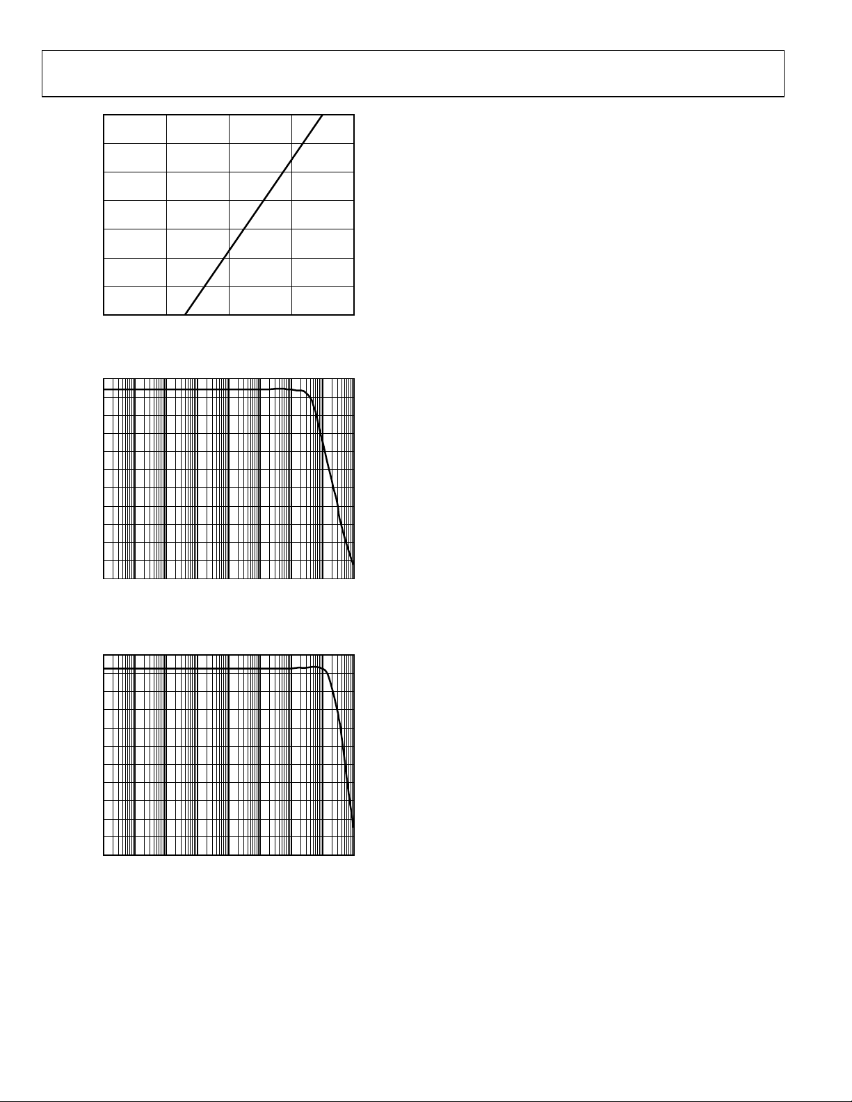
1 10 100 1k 10k 100k 1M 10M 100M
220
200
180
160
140
120
100
GM (μA/V)
80
60
40
20
0
1 10 100 1k 10k 100k 1M 10M 100M
Figure 12. C
VOLTAGE (V)
Figure 10. Current Limit
BANDWIDTH
Figure 11. V
Transconductance
CMP
BANDWIDTH
and S
CMP
Transconductance
CMP
05405-010
05405-011
05405-012
VOLTAGE ERROR AMPLIFIER
This is a high gain transconductance amplifier that takes its
input from the load voltage trim stage described previously. The
amplifier requires only the output pin for loop compensation,
which typically consists of a series RC network-to-common. A
parallel resistor may be added to common to reduce the openloop gain and thereby provide some output voltage droop as
output current increases. The output of the amplifier is typically
connected to an emitter follower that drives an optocoupler,
which in turn controls the duty of the primary side PWM. The
emitter follower should have a high gain to minimize loading
effects on the amplifier. Alternatively, an op amp voltage
follower may be used. See
Figure 11.
MAIN VOLTAGE REFERENCE
A 1.5 V reference is connected to the inverting input of the
voltage error amplifier. This 1.5 V reference is the output
voltage of the soft-start circuit. Under closed-loop conditions,
the voltage at the noninverting input is also controlled to 1.5 V.
During start-up, the output voltage should be ramped up in a
linear fashion at a rate that is independent of the load current.
This is achieved by digitally ramping up the reference voltage by
using a counter and a DAC. The ramp rate is configurable via
the SMBus. See
Figure 13.
CURRENT-SENSE AMPLIFIER
This is a two-stage differential amplifier that achieves low offset
and accuracy. The amplifier has the option to be chopped to
reduce offset or left as a linear amplifier without chopping.
Refer to the
gain can be selected from three ranges. It is followed by a trim
stage and then by a low gain buffer stage that can be configured
with a gain of 1.0 or 2.1. The result is a total of six overlapping
gain ranges (65 to 230), one of which must be selected via the
SMBus. This gives ample adjustment to compensate for the
poor initial tolerance of the resistance wires typically used for
current sensing. It also allows selecting a higher sensitivity for
better efficiency or a lower sensitivity for better accuracy (lower
offset). The amplifier offset voltage is trimmed to zero in a
once-off operation via the SMBus and uses a voltage-controlled
current source at the output of the first gain stage. A second
controlled current source is used to trim out the additional
offset due to the mismatch of the external divider resistors. This
offset trim is dynamically adjusted according to the commonmode voltage present at the top of the voltage dividers. Six
ranges are selectable according to the magnitude and polarity of
this offset component. Because the offset compensation circuit
itself has some inaccuracies, the best overall current-sense
accuracy is obtained by using more closely matched external
dividers and then selecting a low compensation range. See
Figure 13.
Register Listing for more details. The amplifier’s
Rev. 0 | Page 20 of 56
Page 21
ADM1041A
CURRENT SENSING
Current is typically sensed by a low value resistor in series with
the positive output of the power supply, positioned just before
the OrFET or diode. For high voltages (12 V and higher), this
resistor is usually placed in the negative load. A pair of closely
matched voltage dividers connected to Pins 2 and 3 divide the
common-mode voltage down to approximately 2.0 V. The
divider ratio must be the same as used in the local and remote
voltage-sense circuits. Alternatively, current may be sensed by a
current transformer (CT) connected to Pin 8. The ADM1041A
must be configured via the SMBus to select one or the other.
See
Figure 13.
CURRENT-TRANSFORMER INPUT
The ADM1041A can also be configured to sense current by
using a CT connected to Pin 8. In this case, the resistive current
sense is disabled. A separate single-ended amplifier has two
possible sensitivities that are selected via the SMBus. If the CT
option is selected, the gain of the 1.0, 2.1 buffer that follows the
gain trim stage is no longer configurable and is fixed at 1.0.
The share driver amplifier has a total of 100 mV positive offset
built into it. To use the device in CT mode, it is necessary to
compensate for this additional 100 mV offset. This is achieved
by adding in a positive offset on the CT input. This also allows
any negative amplifier offsets in the CT chain to be nulled out.
This offset cancellation is achieved by sourcing a current
through a resistance on the ICT pin. The resistor value is 40 kΩ
and so for 100 mV of offset cancellation a current of 2.5 μA is
CURRENT
OrFET GATE
OrFET SOURCE
required. It is possible to fine trim this current via Register 15h,
Bits 4–0, step size 170 nA. For example, 2.5 μA ≈ 15 × 170 nA;
so the code for Register 15h is decimal 15 or 0Fh. Refer to the
Current Transformer parameter in the Specifications table for
more details. See
Figure 13.
CURRENT-SENSE CALIBRATION
Regardless of which means is used to sense the current, the end
result of the calibration process should produce the standard
current share signal between Pins 20 and 23, that is, 2.0 V at
100% load, excluding any additional share signal offset that
might be configured.
CURRENT-LIMIT ERROR AMPLIFIER
This is a low gain transconductance amplifier that takes its
input from one of the calibrated current stages described
previously. The amplifier requires only the output pin for loop
compensation, which typically consists of a series RC networkto-common. A trimmable reference provides a wide range of
adjustment for the current limit. When the current signal
reaches the reference voltage, the output of the error amplifier
comes out of saturation and begins to drive a controlled current
source. The control threshold is nominally 1.0 V. This current
flows through a resistor in series with the trimmed voltage loop
signal and thereby attempts to increase the voltage signal above
the 1.5 V reference for that loop. The closed voltage loop reacts
by reducing the power supply’s output voltage and this results in
constant current operation. See
Figure 13.
TRANSFORMER
CURRENT-
SENSE
CONFIGURATION
CURRENT
TRANSFORMER
V
GAIN = 10
+
C
S
3
2
–/FS
C
S
ICT
8
C
CMP
4
40kΩ
REG 17h b7
IRS/ICT
SET GAIN
SET
CURRENT
SHARE
1.25V
0.5V
CURRENT-
SET CURRENT-
COMPARATOR
SHARE
OFFSET
(V
SHARE
IOUT = 0)
LIMIT LEVEL
OCP
REFVDD
,
TO CURRENTSHARE DRIVE
AMPLIFIER
9R
CURRENT
LIMIT TO
CURRENT
ERROR AMP
OCP
VOLTAGE
ERROR AMP
05405-013
R
V
REF
Figure 13. Current Sense
Rev. 0 | Page 21 of 56
Page 22

ADM1041A
V
OVERCURRENT PROTECTION
When the current limit threshold is reached, the OCP comparator detects when the current error amplifier comes out of
saturation. Its threshold is nominally 0.5 V. This starts a timer
that, when it times out, causes an OCP condition to occur and
the power supply to shut down. If the current limit disappears
before the time has expired, the timer is reset. The time period
is configurable via the SMBus. Undervoltage blanking is applied
during the timer operation. See
CURRENT SHARE
The current-share method is the master–slave type, which
means that the power supply with the highest output current
automatically becomes the master and controls the share bus
signal. All other power supplies become slaves, and the share
bus signal causes them to increase their output voltages slightly
until their output currents are almost equal to that of the
master. This scheme has two major advantages. A failed master
power supply simply allows one of the slaves to become the new
master. A short-circuited share signal disables current sharing,
but all power supplies default to their normal voltage setting,
allowing a certain degree of passive sharing. Because this chip
uses a low voltage process, an external bidirectional amplifier is
needed for most existing share bus signal levels. The voltage
between Pins 20 and 23 is always controlled to 2.0 V full scale,
ignoring any offset. By connecting Pins 20 and 23 together, the
chip can produce a 2.0 V share signal directly without any
external circuits. To improve accuracy, the share signal is
referenced to the remote voltage sense negative (VS-) pin.
3V
2V
SHARE
1V
020040 60 80 100%
Figure 14. Load Share Characteristic
CURRENT-SHARE OFFSET
To satisfy some customer specifications, the current-share
signal can be offset by a fixed amount by using a trimmable
current generator and a series resistor. The offset is added
on top of the 2.0 V full-scale, current-share output signal.
See
Figure 15.
I
DRIVE AMPLIFIER
SHARE
This amplifier is a buffer with enough current source capability
to drive the current-share circuits of several slave power
supplies. It has negligible current sink capability. Refer to the
Differential Sense Amplifier section.
Figure 15.
OFFSET
I
OUT
05405-015
DIFFERENTIAL SENSE AMPLIFIER
This amplifier has unity gain and senses the difference between
the share bus voltage and the remote voltage sense negative pin.
When the power supply is the master, it forms a closed loop
with the I
therefore it causes the share bus voltage between Pins 20 and 23
to equal the current-share signal at the noninverting input of
the I
SHARE
output of the differential-sense amplifier exceeds the internal
current share signal, which causes the I
be driven into cutoff. Because it is not possible to trim out
negative offsets in the op amps in the current-share chain, a
50 mV voltage source is used to provide a known fixed positive
offset. The share bus offset controlled current source must be
trimmed via the SMBus to take out the resulting overall offset.
Figure 15.
See
I
ERROR AMPLIFIER
SHARE
This is a low gain transconductance amplifier that measures the
difference between the internal current share voltage and the
signal voltage on the external share bus. If two power supplies
have almost identical current-share signals, a 50 mV voltage
source on the inverting input helps arbitrate which power
supply becomes the master and prevents hunting between
master and slave roles. The amplifier requires only the output
pin for loop compensation, which typically consists of a series
RC network to common. When the power supply is a slave, the
output of the error amplifier comes out of saturation and begins
to drive a controlled current sink. The control threshold is
nominally 1.0 V. This current flows from a resistor in series
with the trimmed voltage loop signal and thereby attempts to
decrease the voltage signal below the 1.5 V reference for that
loop. The closed voltage loop reacts by increasing the power
supply’s output voltage until current share is achieved. The
maximum current sink is limited so that the power supply
voltage can be increased only a small amount, which is usually
limited to be within the customer’s specified voltage regulation
limit. This small voltage increase also limits the control range of
the current-share circuit and is called the capture range. The
capture range may be set via the SMBus to one of four values,
from 1% to 4% nominal. See
I
CLAMP
SHARE
This clamp keeps the current share-loop compensation
capacitor discharged when the current share is not required to
operate. The clamp is released during power-up when the
voltage reference and therefore the output voltage of the power
supply has risen to either 75% or 88% of its final value. This is
configurable via the SMBus. When the clamp is released, the
current share loop slowly walks in the current share and helps
to avoid output voltage spikes during hot swapping. See
Figure 15.
drive amplifier described previously, and
SHARE
drive amplifier. When the power supply is a slave, the
drive amplifier to
SHARE
Figure 15.
Rev. 0 | Page 22 of 56
Page 23

ADM1041A
SHARE_OK DETECTOR
Incorrect current sharing is a useful early indicator that there is
some sort of noncatastrophic problem with one of the power
supplies in a parallel system. Two comparators are used to
detect an excessive positive or negative error voltage at the input
TO VOLTAGE ERROR AMP
V
REFVDD
,
SHARE
LIMIT LEVEL
9R
R
SHAREOK
CURRENT-
V
ERROR AMP
REF
FROM
CURRENT
SENSE
CURRENT-
SHARE
OFFSET
(V
IOUT = 0)
SET CURRENT-
of the I
share loop has lost control. One of four possible error levels
must be configured via the SMBus. See
I
ERROR
SHARE
AMPLIFIER
error amplifier, which indicates that the current
SHARE
Figure 15.
SCMP
22
I
SHARE
CLAMP
DRIVE
I
SHARE
AMPLIFIER
DIFFERENTIAL
SENSE
50mV50mV
60μA
SHRO
24
23
SHRS+
V
–/SHRS–
S
20
GAIN = (R1+R2)/R2
+12V
GAIN = (R1 + R2)/R2
SHARE BUS
1N4148
R1
R2
REMOTE
–VE SENSE
CURRENT LIMIT
DIFF. VOLTAGE SENSE
CURRENT SHARE
70μA
1V 3V
CAPTURE
V
REF
RAMP UP
ERROR AMP
SOFT-
START
VOLTAGE
V
CMP
5
05405-014
Figure 15. Current-Share Circuit and Soft Start
Rev. 0 | Page 23 of 56
Page 24
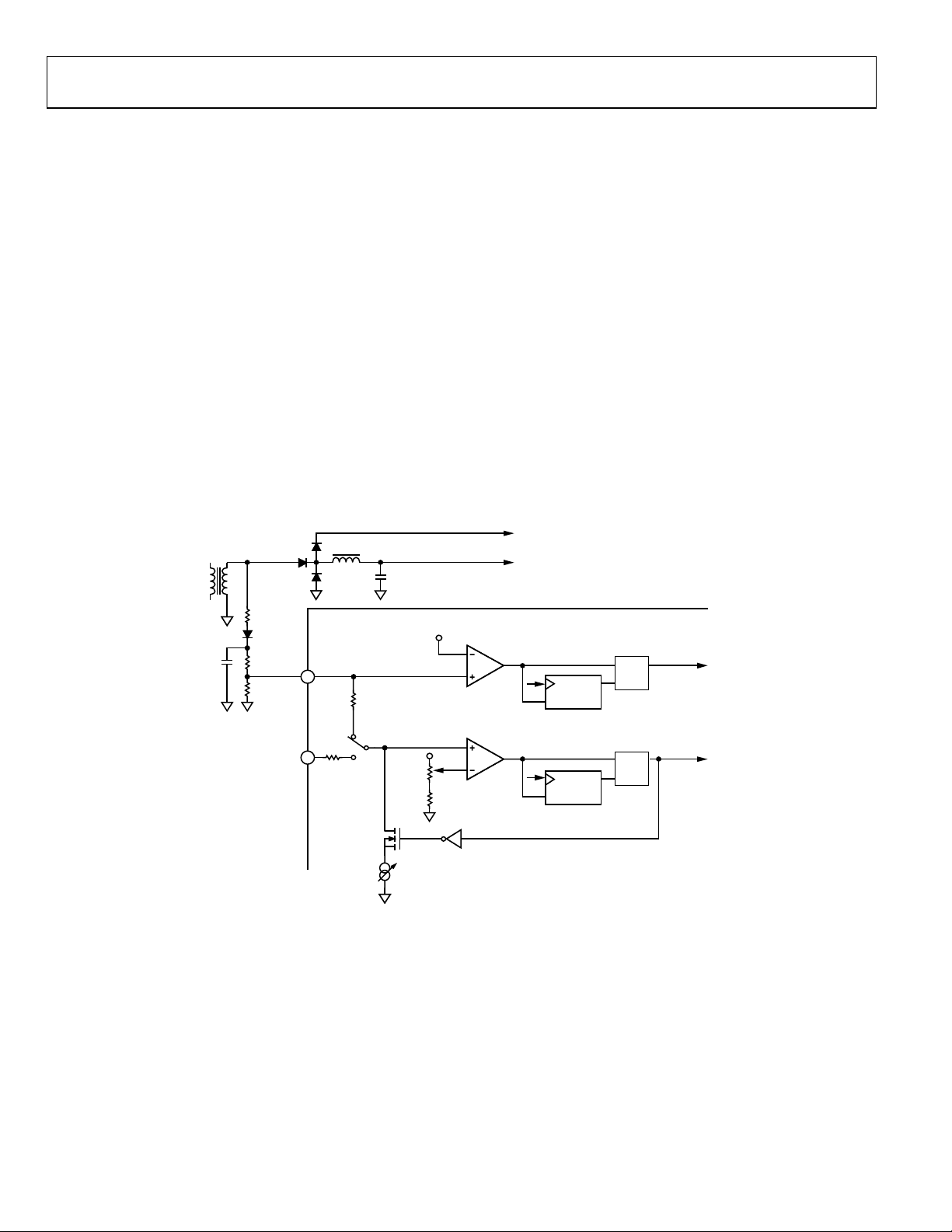
ADM1041A
PULSE/AC
When configured, PULSE and AC
the power main transformer. See
PULSE
Providing the output of the pulse function (PULSE_OK) is
high, the FET in the OR’ing circuit can be turned on. If the
pulses stop for any reason, about 1 second later the PULSE_OK
goes low and the OrFET drive is disabled. This delay allows
passage of all expected pulse skipping modes that might occur
in no load or very light load situations. See
AC
This is rarely used to measure the ac input to the supply
directly. AC
indirectly, the voltage across the bulk capacitor so that the
system can be signaled that power is normal. Also if power is
actually lost, AC
for an orderly shutdown of the power supply. See
SENSE
SENSE
SENSE
2
monitor the output of
SENSE
Figure 16.
Figure 16.
1 or AC
SENSE
2 are usually used to measure,
SENSE
represents when just enough energy is left
Figure 16.
The ac sense function monitors the amplitude of the incoming
pulse and, if sufficiently high, generates a flag to indicate that
the ac, or strictly speaking, the voltage on the bulk capacitor, is
okay. Because the envelope of the pulse has a considerable
amount of 100 Hz ripple, hysteresis is available on this input
pin. Internally there is a 20 μA to 80 μA current sink. With a
909R external Thevenin resistance, this current range translates
to a voltage hysteresis of 200 mV to 500 mV. The internal
hysteresis current is turned off when the voltage exceeds the
reference on the comparator. This form of hysteresis allows
simple scaling to be implemented by changing the source
impedance of the pulse-conditioning circuit. Some trimming
of hysteresis and threshold voltage is provided. The ac sense
function can be configured to be derived from AC
than AC
locations to be used to generate AC_OK for better flexibility
or accuracy.
TO OrFET SOURCE
1. This allows a separate dc input from various
SENSE
SENSE
2 rather
AC
AC
SENSE
PULSE
SENSE
TO CURRENT-
SENSE RESISTOR
AND OrFET GATE
0.525V
PULSEOK
S
9
5.3kΩ
5.3kΩ
SELECT
AC
SENSE
1.5V
TRIM
HYSTERESIS
Figure 16. Pulse In and AC
SENSE
1
10
2
Circuit
R
R
CLK
1 SEC
CLK
1 mS
Q
Q
Q
R
S
R
AC_OK
Q
05405-016
Rev. 0 | Page 24 of 56
Page 25

ADM1041A
OrFET GATE DRIVE
When configured, this block provides a signal to turn on/off
an OrFET used in the output of paralleled power supplies. The
gate drive voltage of one of these FETs is typically 6 V to 10 V
above the output voltage. Because the output voltage of the
ADM1041A is limited, an external transistor needs to be used.
The block diagram shows an example of this approach.
Figure 21.
See
output is an open-drain, N-channel MOSFET and is
The F
G
normally high, which holds the OrFET off. When all the startup conditions are correct, Pin 19 is pulled low, which allows the
OrFET to turn on. The logic can also be configured as inverted
if a noninverting drive circuit is used.
Figure 19 and Figure 20 show the OrFET turn-off time and
turn-on time when the F
seen, to turn off the OrFET, the V
pin polarity is inverted. As can be
G
pin now transitions from
FG
high to low. Also, its corresponding turn-on event occurs from
a low-to-high transition. The circuit in Figure 21 is used to
generate these plots.
A differential amplifier monitors the voltage across the OrFET
and has two major functions. First, during start-up, it allows the
OrFET to turn on with almost 0 V across it to avoid voltage
glitches on the bus. This applies to a hot bus or a cold bus. The
internal threshold can be configured from 20 mV to 50 mV
(negative), which is scaled up by the external voltage dividers.
Second, if a rectifier or filter capacitor fails during steady state
operation, it detects the resulting reverse voltage across the
OrFET’s on-resistance and turns off the OrFET before a voltage
dip appears on the bus. The internal threshold can be
configured from 100 mV to 250 mV (negative), which is also
scaled up by the external voltage dividers. A slightly larger filter
capacitor may be used on the voltage divider at Pin 6 to speed
up this function.
Figure 17 shows the typical response time of the ADM1041A to
such an event. In the plot, V
time of the F
pin to a reverse voltage event on the FD pin is
G
is ramped down and the response
FD
seen. This simulates the rectifier or filter capacitor failure
during steady-state operation. When the F
1.9 V (2 V minus 100 mV threshold), the F
voltage is below
D
pin reacts. As can
G
be seen, the response time is approx 330 nsecs. This extremely
fast turn-off is vital in an n+1 power supply system
configuration. It ensures that the damaged power supply
removes itself from the system quickly.
Figure 18 shows the
equivalent response time to turn on the OrFET. As can be seen,
there is a delay of approximately 500 ns before the FG pin
ramps down to turn on the OrFET, allowing the power supply
to contribute to the system. This propagation delay is due
mainly to internal amplifier response limitations. The circuit in
Figure 21 is used to generate these plots. In this case, the
resistor to V
from the FG pin is 2 kΩ.
DD
T
= 330ns
TOTAL
64%
T
= 218ns T= 112ns
DELAY
Figure 17. OrFET Turn-Off Time (Default Polarity)
T
= 506ns
TOTAL
Figure 18. OrFET Turn-On Time (Default Polarity)
05405-017
05405-018
Rev. 0 | Page 25 of 56
Page 26

ADM1041A
T
TOTAL
= 222ns
05405-019
T
= 618ns
TOTAL
T
= 506ns T = 112ns
DELAY
64%
05405-020
Figure 19. OrFET Turn- Off Time (Inverse Polarity)
CURRENT
62
FDFS
PULSEOK
LOADOK
REVERSEOK
RESET
VOLTAGE
DETECTOR
PENOK
V
REF
Figure 20. OrFET Turn-On Time (Inverse Polarity)
V
OUT
DRAINSOURCE
V = V
OrFET OK
OUT
+10V
POLARITY
GATE
V
DD
F
G
19
05405-021
Figure 21. OrFET Gate Drive Circuit
Rev. 0 | Page 26 of 56
Page 27

ADM1041A
OSCILLATOR AND TIMING GENERATORS
An on-board oscillator is used to generate timing signals. Some
trimming of the oscillator is provided to adjust for variations in
processing.
All timing generated from the oscillator is expected to meet the
same tolerances as the oscillator. Because individual delay
counters are generally two to three bits, the worst error is one
clock period into these counters, which is 25% of the nominal
delay period. None of these tolerances are extremely critical.
LOGIC I/O AND MONITOR PINS
Apart from pins required for the various key analog functions, a
number of pins are used for logic level I/O signals. If the logic
I/O function is not required, the pins may be reconfigured as
general-purpose comparators for analog level monitoring
(MON) and may be additionally configured to have typical
OVP and UVP properties, either positive-going or negativegoing, depending on whether a positive supply output or a
negative supply output is being monitored. The status of all
protection and monitoring comparators is held in registers that
can be read by a microprocessor via the SMBus. Certain control
bits may be written to via the SMBus.
CBD/ALERT
This pin can be used either as a crowbar driver or as an SMBus
alert signal to indicate that a fault has occurred. It is typically
configured to respond to a variety of status flags, as detailed in
Registers 1Ah and 1Bh. The primary function of this pin is as a
crowbar driver, and as such it should be configured to respond
to the OV fault status flag. It can be configured to respond to
any or all of a variety of fault status flags, including a microprocessor writable flag, and can be configured as latching or
nonlatching. It may also be configured as an open-drain
N-channel or P-channel MOSFET and as positive or negative
(inverted) logic. A pull-up or pull-down resistor is required.
This pin may be wire-OR’ed with the same pin on other
ADM1041A’s in the power supply.
The alternative function is an SMBus alert output that can be
used as an interrupt to a microprocessor. If a fault occurs, the
microprocessor can then query the ADM1041A(s) about the
fault status. This is intended to avoid continuously polling the
ADM1041A(s).
MON1
This is the alternative analog comparator function for the
Pulse/AC
MON1 is selected, AC
1 pin (Pin 9). The threshold is 1.25 V. When
SENSE
1 defaults to true.
SENSE
MON2
This is the alternative analog comparator function for the
2 pin (Pin 10). The threshold is 1.25 V. When MON2 is
AC
SENSE
selected, AC
2 defaults to true.
SENSE
PEN
This is the power enable pin that turns the PWM converter on
and can be configured as active high or low. This might drive an
opto-isolator back to the primary side or connect to the enable
pin of a secondary-side post regulator.
PSON
This pin is usually connected to the customer’s PSON signal
and, when asserted, causes the ADM1041A to turn on the
power output. It can be configured as active high or low.
Alternatively, a microprocessor can communicate the PSON
function to the ADM1041A using the SMBus, or the PS
LINK
ON
signal may be used. When the PSON pin is not used as such, it
can be configured as an analog input, MON3.
MON3
This is the alternative analog comparator function for the PSON
pin (Pin 16). The threshold is 1.25 V. When MON3 is selected,
PSON defaults to off.
DC_OK (POWER-OK, POWER Good, Etc.)
This output is true when all dc output voltages are within
tolerance and goes false to signify an imminent loss of power.
(Timing is programmable, see the register description). It
can be configured as an open-drain, N-channel or P-channel
MOSFET and as positive or negative (inverted) logic. A pull-up
or pull-down resistor is required. This pin may be wire-OR’ed
with the same pin on other ADM1041As in the power supply.
When the DC_OK pin is not used as such, it can be configured
as an analog input, MON4.
MON4
This is the alternative analog comparator function for the
DC_OK pin (Pin 17). The threshold is 1.25 V.
Routinely, the microprocessor needs to gather other data
from the ADM1041A(s), which can include the fault status,
so the ALERT function may not be used. Also, the simplest
microprocessors may not have an interrupt function. This
allows the CBD/ALERT pin to be used for other functions.
Rev. 0 | Page 27 of 56
Page 28
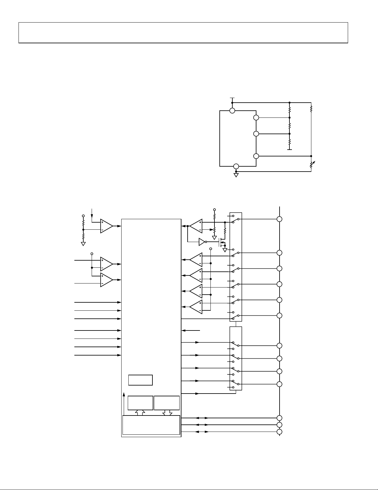
ADM1041A
S
K
AC_OK
This output is true when either AC
(configurable). It can be configured as an open-drain,
N-channel or P-channel MOSFET and as positive or negative
(inverted) logic. A pull-up or pull-down resistor is required.
This pin can be wire-OR’ed with the same pin on other
ADM1041As in the power supply. When the AC_OK pin is not
used as such, it can be configured as an analog input, MON5, or
as a voltage reference.
MON5
This is the alternative analog comparator function for the
AC_OK pin (Pin 18). The threshold is 2.5 V, and it has a
100 μA current source that allows hysteresis to be controlled by
adjusting the external source resistance. It is ideal for an OTP
sensing circuit using a thermistor as part of a voltage divider.
The OTP condition can be configured to latch off the power
supply (similar to OVP) or to allow an autorestart (soft OTP).
Figure 22.
See
OCP
2.5V
SENSE
1 or AC
OCP
SENSE
2 is true
MON5
In Figure 22, MON2 and MON3 are configured to monitor a
negative 12 V rail. MON2 is configured as negative-going OVP,
and MON3 is configured as positive-going UVP. The 5 V power
rail is used for bias voltage.
+5V
1
V
CC
7
MON2
MON3
MON5
10
16
18
–12V
THERMISTOR
05405-022
Figure 22. Example of MON Pin Configuration
2.5V
OTP/
18
MON5
OVP
UVP
ACOK
ORFETOK
HAREO
RESET
V
OK
DD
V
OV
DD
PENOK
1.5V
1.25V
OVP
UVP
ACOK
ORFETOK
SHAREOK
RESET
VDDOK
VDDOV
PENOK
CONTROL
REGISTERS
PWRON
CONFIGURE
(WRITE
REGISTERS)
CONTROL
LINES
GENERAL
LOGIC
SERIAL
INTERFACE
MON1
MON2
MON3
MON4
PSON
CLOCK
AC_OK
DC_OK
CBD
PEN
CONFIGURE
I/Os
STATUS
(READ
REGISTERS)
PEN
SCL
CS
Figure 23. Block Diagram of Protection and General Logic
9
MON1
10
MON2
16
MON3
17
MON4
16
PSON
18
AC_OK
17
DC_OK
11
CBD/ALERT
12
PEN
SDA/
14
PS
SCL/
13
AC_OKLink
15
ADD0
LINK
ON
05405-023
Rev. 0 | Page 28 of 56
Page 29

ADM1041A
(11)
CBD/
ALERT
CMP
(5)
V
GM
VOLTAGE
REF
ERROR AMP
V
set_cshare_clamp
SCL/
AC_OKLink
scl_in
error_amp
inv input
OUT
V
1.5V
SOFT-
START
SOFT-
ssr1s1, ssrs0
(13)
CMP
(22)
S
scmp_in
75%/88%
DAC
RAMP
START
300μs, 10ms, 20ms, 40ms
sda_in
SDA/
LINK
PS
clamp
m_shr_clmp
(14)
ON
sda_out
(12)
PEN
DRIVER
polpen
m_penok_r
gatepen
SQ
R
gateramp
vddok
(17)
MON4
DC_OK/
DRIVER
m_dcok_r
poldcok, mn4s0
POKTS1, POKTS0
DC_OK ON DELAY
200, 400, 800, 1600ms
FAULTB
QR
SQ
FAULT
NOT USED
selcbd2<0>
polcbd
mfg5
selcbd2<1>
DRIVER
cbdlm
m_cbd_w
selcbd2<2>
mfg4
selcbd2<3>
S
DQ
mfg3
R
m_cbd_cir
mfg2
selcbd2<4>
selcbd2<5>
por
mfg1
selcbd2<6>
vddok
selcbd2<7>
mn1s
i2cmb
m_acsns_w
SENSE
AC
acss
CONFIG
1/
SENSE
MON1
AC
acsns
(9)
acsok
mn2s
uvbm
1ms
DEBOUNCE
acsns_hyst
CONFIG
2/
SENSE
MON2
AC
psonlink
psonts1.psonts0
m_pson_w
acsns_thresh
(10)
m_pson_r
mn3s
PSON3/
up_pson_m
0, 40, 80, 160ms
mov5
CONFIG
(12)
MON3
softotp
restartb
rsm
penon
m_psonok_r
dcokoff_delay
1 SECOND
Figure 24. General Logic
QS
0, 1, 2, 4ms
DC_OK OFF DELAY
opt(mov5)
selcbd1<2>
selcbd1<1>
OR 1, 2, 3, 4SEC
128, 256, 384, 512μs,
OCP RIDETHROUGH
ocpf
ovfault
orfetok
shareok
selcbd1<0>
uvfault
uvok
R
450μs
UV BLANK
UV DEBOUNCE
muv3
muv5
muv4
muv1
muv2
localuv
ERROR AMP
OF CURRENT-
FROM OUTPUT
80ms
OCP
COMP
ocfault
OCP
OCPF
(4)
ocpts2, ocpts1, ocpts0
DISABLE
0.5V
curr_lim_dis
acsns
selcbd1<3>
mov1
mov5
softotp
ocpto
selcbd1<5>
selcbd1<4>
mov2
mov3
uvfault
selcbd1<6>
mov4
vddov
ovfault
selcbd1<7>
local ov
05405-024
Rev. 0 | Page 29 of 56
Page 30

ADM1041A
SMBus SERIAL PORT
The programming and microprocessor interface for the
ADM1041A is a standard SMBus serial port, which consists of a
clock line and a data line. The more rigorous requirements of
the SMBus standard are specified in order to give the greatest
noise immunity. The ADM1041A operates in slave mode only.
If a microprocessor is not used, these pins can be configured to
perform the PS
this port is not intended to be connected to the customer’s
SMBus (or I
bus fault interferes with the interpart communication, possibly
preventing proper operation and proper fault reporting. If the
customer needs status and control functions via the SMBus, it is
recommended that a microprocessor with a hardware SMBus
2
C) port be used for this interface. The microprocessor should
(I
access the ADM1041As via a second SMBus port, which may be
emulated in software (subset of the full protocol).
MICROPROCESSOR SUPPORT
The ADM1041A has many features that allow it to operate with
the aid of a microprocessor. There are several reasons why a
microprocessor might be used:
• To provide unusual logic and/or timing requirements,
particularly for fault conditions.
• To drive one or more LEDs, including flashing, according
to the status of the power supply.
• To replace other discrete circuits such as multiple OTP,
extra output monitoring, fan speed control, and failure
detection, and combine the status of these circuits with the
status of the ADM1041As.
• To free up some pins on the ADM1041As. This could
reduce the BOM and therefore the cost.
• To interface to an external SMBus (or I
detailed status reporting. The SMBus port in the
ADM1041A is not intended for this purpose.
• To allow EEPROM space in ADM1041A(s) or in the
microprocessor to be used for FRU (VPD) data. A simple
or complex microprocessor can be used according to the
amount of additional functionality required. Note that the
microprocessor is not intended to access or modify the
EEPROM address space that is used for the configuration
of the ADM1041A(s).
LINK and AC_OKLink functions. Note that
ON
2
C bus). Continuous SMBus activity or an external
2
C) for more
Interfacing
The microprocessor must access the ADM1041A(s) via their
2
on-board SMBus (I
C) port. Because this port is also used to
configure the ADM1041A(s), the software must include a
routine that avoids SMBus activity during configuration. The
simplest interface is for the microprocessor to have an SMBus
2
C) port implemented in hardware, but this may be more
(I
expensive. An alternative is to emulate the bus in software and
to use two general-purpose logic I/O pins. Only a simple subset
of the SMBus protocol need be emulated because the
ADM1041A always operates as a slave device.
Configuring for a Microprocessor
Except during initial configuration, all ADM1041A registers
that need to be accessed are high speed CMOS devices that do
not involve EEPROM.
Table 43, the Microprocessor Support
table describes the various registers, bits, and flags that can be
read and written to.
Note that for the microprocessor to gain control of the PSON
and AC
functions, Reg12h (Table 27) must be configured.
SENSE
A separate configuration bit is allocated to each signal. The
microprocessor can then write to the signal as though the
signal originated within the ADM1041A itself.
BROADCASTING
In a power supply with multiple outputs, it is recommended
that all outputs rise together. Because the SMBus is relatively
slow, writing sequentially to the PSON signal in each
ADM1041A, for instance, causes a significant delay in the
output rise of the last chip to be written. The ADM1041A
avoids this problem by allocating a common broadcast address
that all chips can respond to. To avoid data collisions, this
feature should be used only for commands that do not initiate a
reply.
SMBus SERIAL INTERFACE
Control of the ADM1041A is carried out via the SMBus. The
ADM1041A is connected to this bus as a slave device under the
control of a master device.
The ADM1041A has a 7-bit serial bus slave address. When the
device is powered up, it does so with a default serial bus
address. The default power-on SMBus address for the device is
1010XXX binary, the three lowest address bits (A2 to A0) being
defined by the state of the address pin, ADD0, and Bit 1 of
Configuration Register 4 (ADD1). Because ADD0 has three
possible states (tied to V
Config4 < 1 > can be high or low, there are a total of six possible
addresses, as shown in
, tied to GND, or floating) and
DD
Tabl e 6.
Rev. 0 | Page 30 of 56
Page 31

ADM1041A
S
A
GENERAL SMBus TIMING
The SMBus specification defines specific conditions for
different types of read and write operations. General SMBus
read and write operations are shown in the timing diagrams of
Figure 25, Figure 26, and Figure 27, and described in the
following sections.
If the operation is a write operation, the first data byte after the
slave address is a command byte. This tells the slave device what
to expect next. It may be an instruction, such as telling the slave
device to expect a block write, or it may be a register address
that tells the slave where subsequent data is to be written.
The general SMBus protocol operates as follows.
The master initiates data transfer by establishing a start
condition, defined as a high-to-low transition on the serial data
line, SDA, while the serial clock line, SCL, remains high. This
indicates that a data stream follows. All slave peripherals
connected to the serial bus respond to the start condition and
shift in the next 8 bits, consisting of a 7-bit slave address (MSB
first), plus an R/
W
bit, which determines the direction of the
data transfer, that is, whether data is written to or read from the
slave device (0 = write, 1 = read).
The peripheral whose address corresponds to the transmitted
address responds by pulling the data line low during the low
period before the ninth clock pulse, known as the Acknowledge
bit, and holding it low during the high period of this clock
pulse. All other devices on the bus remain idle while the
selected device waits for data to be read from or written to it. If
W
the R/
the R/
bit is a 0, then the master writes to the slave device. If
W
bit is a 1, the master reads from the slave device.
Data is sent over the serial bus in sequences of nine clock
pulses, eight bits of data, followed by an Acknowledge bit from
the slave device. Data transitions on the data line must occur
during the low period of the clock signal and remain stable
during the high period, because a low-to-high transition when
the clock is high may be interpreted as a stop signal.
Because data can flow in only one direction as defined by the
W
bit, it is not possible to send a command to a slave device
R/
during a read operation. Before doing a read operation, it might
first be necessary to perform a write operation to tell the slave
what sort of read operation to expect and/or the address from
which data is to be read.
When all data bytes have been read or written, stop conditions
are established. In write mode, the master pulls the SDA line
high during the tenth clock pulse to assert a stop condition. In
read mode, the master device releases the SDA line during the
low period before the ninth clock pulse, but the slave device
does not pull it low. This is known as No Acknowledge. The
master then takes the data line low during the low period before
the tenth clock pulse, then high during the tenth clock pulse to
assert a stop condition.
Note: If it is required to perform several read or write
operations in succession, the master can send a repeat start
condition instead of a stop condition to begin a new operation.
19 1 99
SCLK
DAT
A6
A5 A4 A3 A2 A1 A0 R/W D7
START BY
MASTER
Figure 25. Writing a Register Address to the Address Pointer Register, then Writing Data to the Selected Register
FRAME 1
SERIAL BUS ADDRESS BYTE
SCLK (CONTINUED)
SDATA (CONTINUED)
ACK. BY
ADM1041A
D7 D6 D5 D4 D3
D6 D5 D4 D3 D2 D1 D0
ADDRESS POINTER REGISTER BYTE
FRAME 2
FRAME 3
DATA BYTE
D2
D1 D0
ACK. BY
ADM1041A
ACK. BY
ADM1041A
91
STOP BY
MASTER
05405-025
Rev. 0 | Page 31 of 56
Page 32
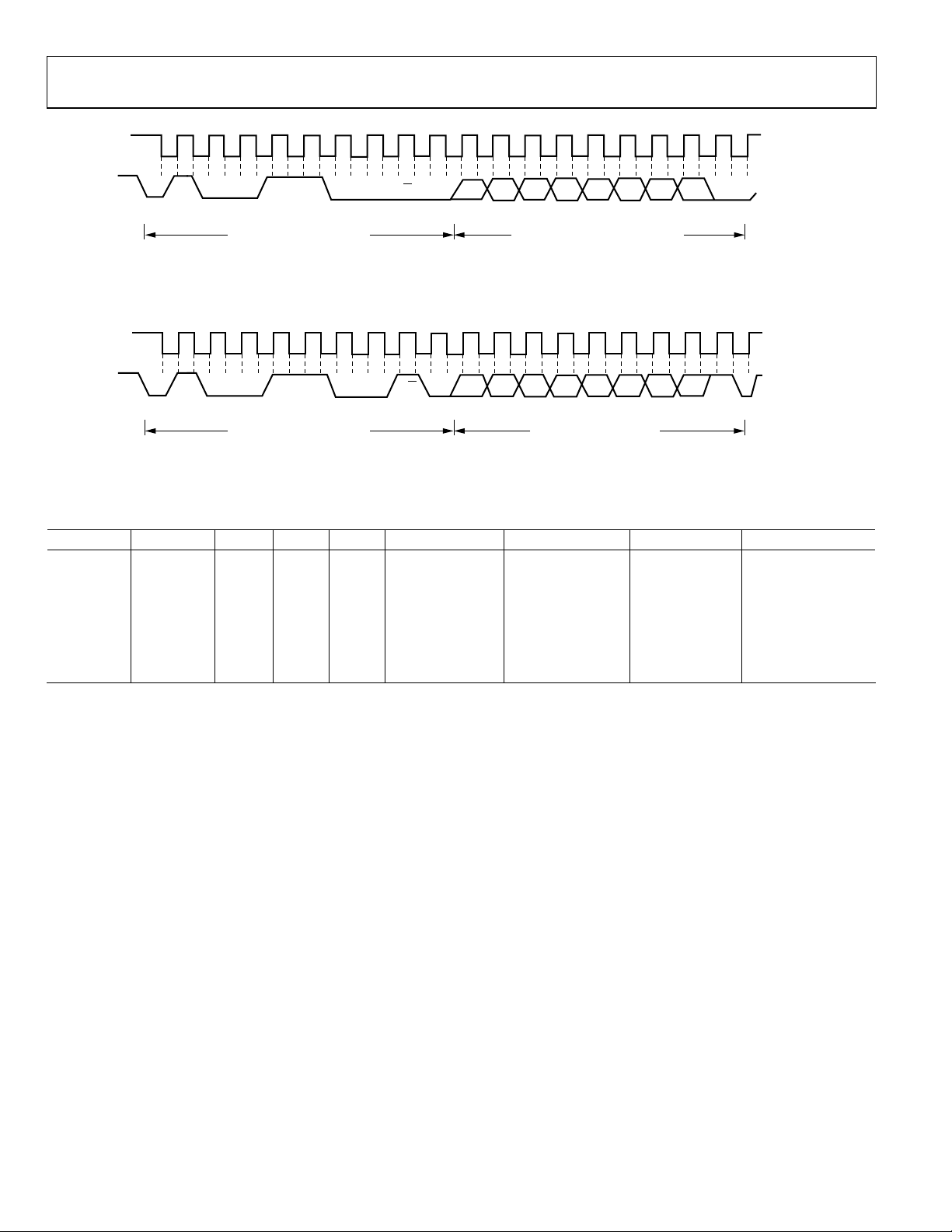
ADM1041A
A
SCLK
SDAT
START BY
MASTER
1199
A6 A5 A4 A3 A2 A1 A0 R/W D7 D6 D5 D4 D3 D2 D1 D0
ACK. BY
FRAME 1
SERIAL BUS ADDRESS BYTE
ADM1041A
ADDRESS POINTER REGISTER BYTE
FRAME 2
ACK. BY
ADM1041A
STOP BY
MASTER
05405-026
Figure 26. Writing to the Address Pointer Register Only
1199
SCLK
SDATA
START BY
MASTER
A6 A5 A4 A3 A2 A1 A0 D7 D6 D5 D4 D3 D2 D1 D0
FRAME 1
SERIAL BUS ADDRESS BYTE
R/W
ACK. BY
ADM1041A
FRAME 2
DATA BYTE FROM ADM1041
ACK. BY
ADM1041A
STOP BY
MASTER
05405-027
Figure 27. Reading Data from a Previously Selected Register
Table 6. Device SMBus Addresses
ADD1 Bit1 ADD0 Pin A2 A1 A0 Target Device ADDRESS HEX READ HEX WRITE
0 GND 0 0 0 0 1010 000X A0 A1
0 VDD 0 0 1 1 1010 001X A2 A3
0 NC 1 0 0 4 1010 100X A8 A9
1 GND 0 1 0 2 1010 010X A4 A5
1 VDD 0 1 1 3 1010 011X A6 A7
1 NC 1 0 1 5 1010 101X AA AB
X X X X X All Devices 1010 111X AE
1
ADD1 is low by default. To access the additional three addresses it is necessary to set Config 4 < 1 > high and then perform a power cycle to allow the new address to
be latched after the EEPROM download. Refer to the section on Extended SMBUS Addressing for more details.
Rev. 0 | Page 32 of 56
Page 33

ADM1041A
SMBus PROTOCOLS FOR RAM AND EEPROM
The ADM1041A contains volatile registers (RAM) and
nonvolatile EEPROM. RAM occupies the address locations
from 00h to 7Fh, while EEPROM occupies the address locations
from 8000h to 813Fh.
S
ADDRESS
SLAVE
COMMAND A2h
W A A PA A
(PAGE ERASE)
Figure 28. EEPROM Page Erase Operation
EEPROM
ADDRESS
HIGH BYTE
(80h OR 81h)
7
EEPROM
ADDRESS
LOW BYTE
(00h TO FFh)
ARBITRARY
A
10811129216435
DATA
05405-028
The SMBus specification defines several protocols for different
types of read and write operations. The protocols used in the
ADM1041A are described and illustrated in this section. The
following abbreviations are used in the diagrams:
S Start
P Stop
R Read
W Write
A Acknowledge
A
No Acknowledge
The ADM1041A uses the following SMBus write protocols.
SMBus Erase EEPROM Page Operations
EEPROM memory can be written to only if it is effectively
unprogrammed. Before writing to one or more locations that
are already programmed, the page containing those locations
must be erased. EEPROM ERASE is performed by sending a
page erase command byte (A2h) followed by the page location
of the item to be erased. (There is no need to set an erase bit in
an EEPROM control/status register.)
The EEPROM consists of 16 pages of 32 bytes each; the register
default EEPROM consists of 1 page of 32 bytes starting at
8100h.
Table 7. EEPROM Page Layout
Page No. EEPROM Location Description
1 8000h to 801Fh Available FRU
2 8020h to 803Fh Available FRU
3 8040h to 805Fh Available FRU
4 8060h to 807Fh Available FRU
5 8080h to 809Fh Available FRU
6 80A0h to 80BFh Available FRU
7 80C0h to 80DFh Available FRU
8 80E0h to 80FFh Available FRU
9 8100h to 811Fh Configuration Boot Registers
10 8120h to 813Fh ADI Registers
11 8140h to 815Fh Available FRU
12 8160h to 817Fh Available FRU
13 8180h to 819Fh Available FRU
14 81A0h to 81BFh Available FRU
15 81C0h to 81DFh Available FRU
16 81E0h to 81FFh ADI Registers
The EEPROM page address consists of the EEPROM address
high byte, 80h for FRU or 81h for register default, and the three
MSBs of the low byte. The lower five bits of the EEPROM
address of the low byte are ignored during an erase operation.
Page erasure takes approximately 20 ms. If the EEPROM is
accessed before erasure is complete, the SMBus responds with
No Acknowledge.
Figure 29 shows the peak IDD supply current during an
EEPROM page erase operation. Decoupling capacitors of 10 μF
and 100 nF are recommended on V
Figure 29. EEPROM Page Erase Peak I
DD
.
05405-029
Current
DD
SMBus Write Operations
Send Byte
In this operation, the master device sends a single command
byte to a slave device, as follows:
1. The master device asserts a start condition on SDA.
2. The master sends the 7-bit slave address followed by the
write bit (low).
3. The addressed slave device asserts ACK on SDA.
4. The master sends a command code.
5. The slave asserts ACK on SDA.
6. The master asserts a stop condition on SDA and the
transaction ends.
In the ADM1041A, the send byte protocol is used to write a
register address to RAM for a subsequent single-byte read from
the same address or block read or write starting at that address.
S
ADDRESS
Figure 30.
SLAVE
W A A P
456213
RAM
ADDRESS
(00h TO 7Fh)
05405-030
This is illustrated in
Figure 30. Setting a RAM Address for Subsequent Read
Rev. 0 | Page 33 of 56
Page 34
ADM1041A
If it is required to read data from the RAM immediately after
setting up the address, the master can assert a repeat start
condition immediately after the final ACK and carry out a
single-byte read, block read, or block write operation without
asserting an intermediate stop condition.
Write Byte/Word
In this operation, the master device sends a command byte and
one or two data bytes to the slave device, as follows:
1. The master device asserts a start condition on SDA.
2. The master sends the 7-bit slave address followed by the
write bit (low).
3. The addressed slave device asserts ACK on SDA.
4. The master sends a command code.
5. The slave asserts ACK on SDA.
6. The master sends a data byte.
7. The slave asserts ACK on SDA.
8. The master sends a data byte (or asserts stop at this point).
9. The slave asserts ACK on SDA.
10. The master asserts a stop condition on SDA to end the
transaction.
In the ADM1041A, the write byte/word protocol is used for
the following three purposes. The ADM1041A knows how to
respond by the value of the command byte.
• Write a single byte of data to RAM. Here, the command
byte is the RAM address from 00h to 7Fh and the (only)
data byte is the actual data, as shown in
4
S
ADDRESS
SLAVE
RAM
ADDRESS
(00h TO 7Fh)
Figure 31. Single-Byte Write to RAM
• Set up a 2-byte EEPROM address for a subsequent read or
block read. In this case, the command byte is the high byte
of the EEPROM address (80h). The (only) data byte is the
low byte of the EEPROM address, as shown in
EEPROM
S
ADDRESS
SLAVE
ADDRESS
W A PA A
HIGH BYTE
(80h OR 81h)
Figure 32. Setting an EEPROM Address
If it is required to read data from the EEPROM immediately after setting up the address, the master can assert a
repeat start condition immediately after the final ACK and
carry out a single-byte read or a block read without
asserting an intermediate stop condition.
Figure 31.
6785213
DATAW A A PA
67852143
EEPROM
ADDRESS
LOW BYTE
(00h TO FFh)
05405-031
Figure 32.
05405-032
• Write a single byte of data to EEPROM. In this case, the
command byte is the high byte of the EEPROM address,
80h or 81h. The first data byte is the low byte of the
EEPROM address and the second data byte is the actual
data. Bit 1 of EEPROM Register 3 must be set. This is
illustrated in
SLAVE
S
ADDRESS
Figure 33.
5
EEPROM
ADDRESS
W A A PA
HIGH BYTE
(80h OR 81h)
Figure 33. Single-Byte Write to EEPROM
691072143
EEPROM
ADDRESS
LOW BYTE
(00h TO FFh)
8
A
DATA
05405-033
If it is required to read data from the ADM1041A immediately
after setting up the address, the master can assert a repeat start
condition immediately after the final ACK and carry out a
single-byte read, block read, or block write operation without
asserting an intermediate stop condition.
Block Write
In this operation, the master device writes a block of data to a
slave device. Programming an EEPROM byte takes
approximately 350 μs, which limits the SMBus clock for
repeated or block write operations. The start address for a block
write must have been set previously. In the case of the
ADM1041A, this is done by a send byte operation to set a RAM
address or by a write byte/ word operation to set an EEPROM
address.
1. The master device asserts a start condition on SDA.
2. The master sends the 7-bit slave address followed by the
write bit (low).
3. The addressed slave device asserts ACK on SDA.
4. The master sends a command code that tells the slave
device to expect a block write. The ADM1041A command
code for a block read is A0h (10100000).
5. The slave asserts ACK on SDA.
6. The master sends a data byte that tells the slave device how
many data bytes are to be sent. The SMBus specification
allows a maximum of 32 data bytes to be sent in a block
write.
7. The slave asserts ACK on SDA.
8. The master sends N data bytes.
9. The slave asserts ACK on SDA after each data byte.
10. The master asserts a stop condition on SDA to end the
transaction.
7
8109216435
DATA 2DATA 1
A DATA N
A
S
ADDRESS
SLAVE
COMMAND A0h
W A A PA A
(BLOCK WRITE)
Figure 34. Block Write to EEPROM or RAM
BYTE
COUNT
05405-034
Rev. 0 | Page 34 of 56
Page 35
ADM1041A
When performing a block write to EEPROM, the page that
contains the location to be written should not be writeprotected (Register 03h) prior to sending the above SMBus
packet. Block writes are limited to within a 32-byte page
boundary and cannot cross into the next page.
SMBus READ OPERATIONS
The ADM1041A uses the following SMBus read protocols.
Receive Byte
In this operation, the master device receives a single byte from a
slave device, as follows:
1. The master device asserts a start condition on SDA.
2. The master sends the 7-bit slave address followed by the
read bit (high).
3. The addressed slave device asserts ACK on SDA.
4. The master receives a data byte.
5. The master asserts NO ACK on SDA.
6. The master asserts a stop condition on SDA and the
transaction ends.
In the ADM1041A, the receive byte protocol is used to read a
single byte of data from a RAM or EEPROM location whose
address has been set previously by a send byte or write byte/
word operation. This is illustrated in
SLAVE
S
ADDRESS
Figure 35. Single-Byte Read from EEPROM or RAM
Figure 35.
46213
DATAR A A5P
05405-035
Block Read
In this operation, the master device reads a block of data from a
slave device. The start address for a block read must previously
have been set. In the case of the ADM1041A, this is done by a
send byte operation to set a RAM address or by a write
byte/word operation to set an EEPROM address. The block read
operation itself consists of a send byte operation that sends a
block read command to the slave, immediately followed by a
repeat start, and a read operation that reads out multiple data
bytes, as follows:
1. The master device asserts a start condition on SDA.
2. The master sends the 7-bit slave address followed by the
write bit (low).
3. The addressed slave device asserts ACK on SDA.
4. The master sends a command code that tells the slave
device to expect a block read. The ADM1041A command
code for a block read is A1h (10100001).
5. The slave asserts ACK on SDA.
6. The master asserts a repeat start condition on SDA.
7. The master sends the 7-bit slave address followed by the
read bit (high).
8. The slave asserts ACK on SDA.
9. The master receives a byte count data byte that tells it how
many data bytes are to be received. The SMBus
specification allows a maximum of 32 data bytes to be
received in a block read.
10. The master asserts ACK on SDA.
11. The master receives N data bytes.
12. The master asserts ACK on SDA after each data byte.
13. The slave does not acknowledge after the Nth data byte.
14. The master asserts a stop condition on SDA to end the
transaction.
S
ADDRESS
71
69435
SLAVE
COMMAND A1h
W A PA A
(BLOCK READ)
Figure 36. Block Read from EEPROM or RAM
S
ADDRESS
SLAVE
10
8
BYTE
A
R
COUNT
11 14122
DATA 1
A DATA N
13
A
05405-036
Rev. 0 | Page 35 of 56
Page 36

ADM1041A
Notes on SMBus Read Operations
The SMBus interface of the ADM1041A cannot load the
SMBUS if no power is applied to the ADM1041A. This
requirement allows a power supply to be disconnected from the
ac supply while still installed in a power subsystem.
When using the SMBus interface, a write always consists of the
ADM1041A SMBus interface address byte, followed by the
internal address register byte, and then the data byte. There are
two cases for a read.
In the first case, if the internal address register is known to be at
the desired address, read the ADM1041A with the SMBus
interface address byte, followed by the data byte read from the
ADM1041A. The internal address pointer increments if a block
mode operation is in progress; data values of 0 are returned if
the register address limit of 7Fh is exceeded or if unused
registers in the address range 00h to 7Fh are accessed. If the
address register is pointing at EEPROM memory, that is 8000h,
and the address reaches its limit of 80FFh, it does not roll over
to Address 8100h on the next access.
Additional accesses do not increment the address pointer, all
reads return 00h, and all writes complete normally but do not
change any internal register or EEPROM location. If the address
register is pointing at EEPROM memory, that is 81xxh, and the
address reaches its limit of 813Fh, it does not roll over to
Address 8140h on the next access.
Additional accesses do not increment the address pointer, all
reads return 00h, and all writes complete normally but do not
change any internal register or EEPROM location. Note that for
byte reads, the internal address does not auto-increment.
In the second case, if the internal address register value is
unknown, write to the ADM1041A with the SMBus interface
address byte, followed by the internal address register byte.
Then restart the serial communication with a read consisting of
the SMBus interface address byte, followed by the data byte read
from the ADM1041A.
SMBus ALERT RESPONSE ADDRESS (ARA)
The ADM1041A CBD/ALERT pin can be configured to
respond to a variety of fault signals and can be used as an
interrupt to a microprocessor. The pins from several
ADM1041As may be wire-OR’ed. When the SMBus master
(microprocessor) detects an alert request, it normally needs to
read the alert status of each device to identify the source of the
alert.
The SMBus ARA provides an easier method to locate the source
of a such an alert. When the master receives an alert, it can send
a general call address (0001100) over the bus. The device asserting the alert responds by returning its own slave address to the
master.
If more than one device asserts an alert, all alerting devices try
to respond with their slave addresses, but an arbitration process
ensures that only the lowest slave address is received by the
master. If the slave device has its alert configured as latching, it
sends a command via the SMBus to clear the latch. The master
should then check if the alert line is still asserted, and, if so,
repeat the ARA call to service the next alert. Note that an
alerting slave does not respond to an ARA call unless it is
configured in SMBus mode (not AC_OKLink/PS
LINK) and
ON
up_pson_m is set. The ADM1041A supports the SMBus (ARA)
function.
SUPPORT FOR SMBus 1.1
SMBus 1.1 optionally adds a CRC8 frame check sequence to
check if transmissions are received correctly. This is particularly
useful for long block read/write EEPROM operations, when the
SMBus is heavily loaded or in a noisy environment. The CRC8
frame can be used to guarantee reliability of the EEPROM.
LAYOUT CONSIDERATIONS
Noise coupling into the digital lines (greater than 150 mV),
overshoot greater than V
and undershoot less than GND
CC,
may prevent successful SMBus communication with the
ADM1041A. SMBus No Acknowledge is the most common
symptom, causing unnecessary traffic on the bus. Although the
SMBus maximum frequency of communication is rather low
(400 kHz max), care still needs to be taken to ensure proper
termination within a system with multiple parts on the bus and
long printed circuit board traces. A 5.1 kΩ resistor can be added
in series with the SDA and SCL lines to help filter noise and
ringing. Minimize noise coupling by keeping digital traces out
of switching power supply areas and ensure that digital lines
containing high speed data communications cross at right
angles to the SDA and SCL lines.
POWER-UP AUTO-CONFIGURATION
After power-up or reset, the ADM1041A automatically reads
the content of a 32-byte block of EEPROM memory that starts
at 8100h and transfers the contents into the appropriate trimlevel and control registers (00h to 1Bh). In this way, the
ADM1041A can be preconfigured with the desired operating
characteristics without the host system having to download the
data over the SMBus. This does not preclude the possibility of
modifying the configuration during normal operation.
Figure 37 shows a block diagram of the EEPROM download at
power-up or power-on reset.
EEPROM
RAM
CONFIGURATION
REGISTERS
POWER UP
Figure 37. EEPROM Download
DIGITAL
TRIM
POTS
DIGITAL
TIMING
CONTROL
05405-037
Rev. 0 | Page 36 of 56
Page 37
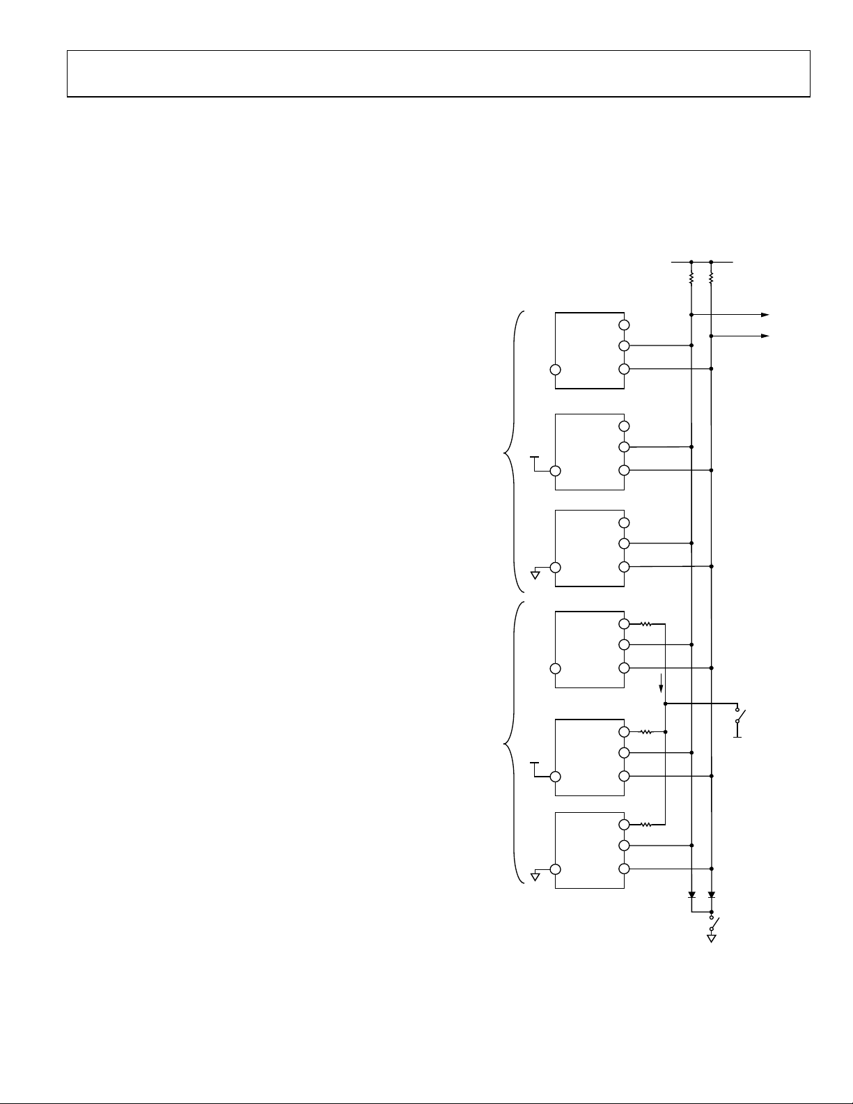
ADM1041A
EXTENDED SMBus ADDRESSING
It is possible to use more than three ADM1041As in a single
power supply. The first time the device is powered up, Bit 1 of
Configuration Register 1 (ADD1) is 0. This means that only
three device addresses are initially available as defined by
ADD0; if there are more than three devices in a system, two or
more of them have duplicate addresses. See
To overcome this, the ICT pin has additional functionality.
Taking ICT below GND temporarily disables the SMBus
function of the device. Thus, if the ICT pin of all devices in
which ADD1 is to remain 0 are taken negative, the ADD1 bits
of all other devices can be set to 1 via the SMBus. Each device
then has a unique address. Internal diodes clamp the negative
voltage to about 0.6 V, and care should be taken to limit the
current to less than approximately 5 mA on each ICT input to
prevent the possibility of damage or latch-up. The suggested
current is 3 mA. One example of a suitable circuit is given in
Figure 38. The ADM1041As can then be configured and
trimmed. If required, AC_OKLink and PS
configured last. If ICT is used for its intended purpose as a
current transformer input, care must be taken with the circuit
design to allow the extended SMBus addressing to work.
SDA/PSONLINK
The SDA pin normally carries data in and out of the
ADM1041A during programming/configuration or while
reading/writing by a microprocessor. If a microprocessor is not
used, this pin can be configured as PS
connected to the same pin on other ADM1041As in the power
supply. If a fault is detected in any ADM1041A, causing it to
shut down, it uses this pin to signal the other ADM1041As to
also shut down. If an auto-restart has been configured, it also
causes all ADM1041As to turn on together.
SCL/AC_OKLink
The SCL pin normally provides a clock signal into the
ADM1041A during programming/configuration or while
reading/writing by a microprocessor. If a microprocessor is not
used, this pin can be configured as AC_OKLink, and can be
connected to the same pin on other ADM1041As in the power
supply. This allows a single ADM1041A to be used for ac
sensing and helps to synchronize the start-up of multiple
ADM1041As.
Figure 38.
LINK must be
ON
LINK and can be
ON
BACKDOOR ACCESS
After SCL and SDA have been configured as AC_OKLink and
LINK, it may be desired to recover the SMBus access to
PS
ON
the ADM1041A. Changes may be necessary to the internal
configuration or trim bits. This is achieved by holding the SCL
and SDA pins at 0 V (ground) while cycling V
then revert to SMBus operation. See
ICT
SCL
N/C
ADD1 = 1
ADD1 = 0
15
V
DD
15
15
15
N/C
V
DD
15
15
ADD0
DEVICE 5
ADD0
DEVICE 4
ADD0
DEVICE 3
ADD0
DEVICE 2
ADD0
DEVICE 1
ADD0
SDA
ICT
SCL
SDA
ICT
SCL
SDA
ICT
SCL
SDA
ICT
SCL
SDA
ICT
SCL
SDA
8
13
14
8
13
14
8
13
14
8
13
14
8
13
14
8
13
14
Figure 38.
4kΩ
2.4mA
4kΩ
4kΩ
. SCL and SDA
DD
V
DD
AC_OKLink
PSONLINK
–12V
EXTENDED
SMBus
ADDRESSING
DEVICE 0
BACKDOOR
05405-038
Figure 38. Extended SMBus Addressing and Backdoor Access
Rev. 0 | Page 37 of 56
Page 38

ADM1041A
REGISTER LISTING
Table 8.
Register Address Name Power-On Value Factory EEPROM Value
00h/2Ah Status1/Status1 Mirror Latched
01h/2Bh Status2/Status2 Mirror Latched
02h/2Ch Status3/Status3 Mirror Latched
03h Calibration Bits From EEPROM Register 8103h 00h
04h Current Sense CC From EEPROM Register 8104h 00h
05h Current Share Offset From EEPROM Register 8105h 00h
06h Current Share Slope From EEPROM Register 8106h FEh
07h EEPROM_lock From EEPROM Register 8107h 20h
08h Load OV Fine From EEPROM Register 8108h 00h
09h Local UVP Trim From EEPROM Register 8109h 00h
0Ah Local OVP Trim From EEPROM Register 810Ah 00h
0Bh OTP Trim From EEPROM Register 810Bh 00h
0Ch ACSNS Trim From EEPROM Register 810Ch 00h
0Dh Config1 From EEPROM Register 810Dh 00h
0Eh Config2 From EEPROM Register 810Eh 00h
0Fh Config3 From EEPROM Register 810Fh 00h
10h Config4 From EEPROM Register 8110h 00h
11h Config5 From EEPROM Register 8111h 00h
12h Config6 From EEPROM Register 8112h 00h
13h Config7 From EEPROM Register 8113h 00h
14h Current Sense Divider Error Trim From EEPROM Register 8114h XXh – Factory Cal Value
15h Current Sense Amplifer Offset Trim From EEPROM Register 8115h XXh – Factory Cal Value
16h Current Sense Options 1 From EEPROM Register 8116h XXh – Factory Cal Value
17h Current Sense Options 2 From EEPROM Register 8117h XXh – Factory Cal Value
18h UV Clamp Trim From EEPROM Register 8118h 00h
19h Load VoltageTrim From EEPROM Register 8119h 00h
1Ah Sel CBD/SMBAlert1 From EEPROM Register 811Ah 00h
1Bh Sel CBD/SMBAlert2 From EEPROM Register 811Bh 00h
1Ch Manufacturer’s ID 41h—Hardwired by manufacturer
1Dh Revision Register Xh—Hardwired by Manufacturer
20h–29h Reserved for Manufacturer
2Ah Status1 Mirror Latched
2Bh Status2 Mirror Latched
2Ch Status3 Mirror Latched
2Dh–2Eh Reserved for Manufacturer
8000h–81FFh EEPROM
XXh—Depends on status of ADM1041A at
power-up.
XXh—Depends on status of ADM1041A at
power-up.
XXh—Depends on status of ADM1041A at
power-up.
XXh—Depends on status of ADM1041A at
power-up.
XXh—Depends on status of ADM1041A at
power-up.
XXh—Depends on status of ADM1041A at
power-up.
Rev. 0 | Page 38 of 56
Page 39

ADM1041A
DETAILED REGISTER DESCRIPTIONS
Table 9. Register 00h, Status1. Power-On Default XXh (refer to the logic schematic in Figure 24 and to Table 43.)
Bit No. Name R/W Description
7 OV Fault R 1= Overvoltage fault has occurred.
6 UV Fault R 1= Undervoltage fault has occurred.
5 OCP Timeout R 1= Overcurrent has occured and timed out (ocpf is in the Status3 Register).
4 Mon1 Flag R 1= MON1 flag.
3 Mon2 Flag R 1= MON2 flag.
2 Mon3 Flag R 1= MON3 flag.
1 Mon4 Flag R 1= MON4 flag.
0 Mon5 Flag R 1= MON5 flag.
Table 10. Register 01h, Status2. Power-On Default XXh (refer to the logic schematic in Figure 24 and to Table 43.)
Bit No. Name R/W Description
7 Share_OK R 1= Current share is within limits.
6 OrFET_OK R 1= OR’ing MOSFET is on.
5 REVERSE_OK R 1= Reverse OK—reverse voltage across the ORing MOSFET is within limits.
4 VDD_OK R 1= VDD is within limits.
3 GND_OK R 1= Connection of GND pin is good.
2 Intref_OK R 1= Internal voltage reference is within limits.
1 Extrefok_OK R 1= External voltage reference is within limits.
0 VDDOV R 1= VDD is above its OV threshold.
Table 11. Register 02h, Status3. Power-On Default XXh (refer to the logic schematic in Figure 24 and to Table 43.)
Bit No. Name R/W Description
7 m_acsns_r R Reflects the status on AC
6 m_pson_r R Reflects the status of PSON.
5 m_penok_r R Reflects the status of PEN.
4 m_psonok_r R Status of PSONLINK.
3 m_DC_OK_r R Status of DC_OK.
2 ocpf R 1= An overcurrent has occured, direct from comparator.
1 PULSE_OK R 1= Pulses are present at the PULSE pin.
0 fault R 1= Fault latch.
Table 12. Register 03h, Calibration Bits. Power-On Default from EEPROM Register 8103h During Power-Up
Bit No. Name R/W Description
7–6 Reverse Voltage Off Threshold
0 0 100 mV
0 1 150 mV
1 0 200 mV
1 1 250 mV
5–4 Reverse Voltage On Threshold
0 0 20 mV
0 1 30 mV
1 0 40 mV
1 1 50 mV
3 PEN_GATE
2 Gate Ramp
R/W
R/W
R/W
R/W
1/AC
SENSE
Reverse Voltage Detector Turn-Off Threshold:
b7 b6 Function
Reverse Voltage Detector Turn On Threshold:
b5 b4 Function
Gate pen option. When set, PEN is gated by AC_OK.
Gate ramp option. When set, soft start is gated by AC_OK.
SENSE
2.
Rev. 0 | Page 39 of 56
Page 40
ADM1041A
Bit No. Name R/W Description
1–0 Load OV Recover
0 0 Add 100 μs delay
0 1 Add 200 μs delay
1 0 Add 300 μs delay
1 1 Add 400 μs delay
Table 13. Register 04h, Current-Sense CC. Power-On Default from EEPROM Register 8104h During Power-Up
Bit No. Name R/W Description
7–3 Current-Limit Trim
2 Reserved
1–0 Share OK Threshold
This register contains the current-sense trim level setting at which current limiting starts. Five
R/W
R/W
R/W
0 0 ±100 mV
0 1 ±200 mV
1 0 ±300 mV
1 1 ±400 mV
Table 14. Register 05h, Current Share Offset. Power-On Default from EEPROM Register 8105h During Power-Up
Bit No. Name R/W Description
7–0 Current Share Offset
This register contains the current-share offset trim level. Writing 00h corresponds to the
R/W
Table 15. Register 06h, Current Share Slope. Power-On Default from EEPROM Register 8106h During Power-Up
Bit No. Name R/W Description
7–1 Current Share Slope
0 Reserved
This register contains current share slope trim level. Increasing this results in a steeper slope
R/W
R/W
Table 16. Register 07h, EEPROM_lock. Power-On Default from EEPROM Register 8107h During Power-Up
Bit No. Name R/W Description
7 Reserved
6 Lock6
5 Lock5
4 Lock4
3 Lock3
2 Lock2
1 Lock1
0 Lock0
R/W
R/W
R/W
R/W
R/W
R/W
R/W
R/W
Don’t Care
Locks 8140h–817Fh Available FRU.
Locks 8120h–813Fh ADI cal registers, locked by manufacturer.
Locks 8100h–811Fh ADM1041A configuration boot registers.
Locks 80C0h–80FFh Available FRU.
Locks 8080h–80BFh Available FRU.
Locks 8040h–807Fh Available FRU.
Locks 8000h–803Fh Available FRU.
Table 17. Register 08h, Load OV Fine. Power-On Default from EEPROM Register 8108h During Power-Up
Bit No. Name R/W Description
7–0 Load OV Trim
Load OV Trim. This range is programmable from 105% to 120% of the nominal load voltage. 00h
R/W
corresponds to 105%. Each LSB results in an increase of 1.6 mV.
Table 18. Register 09h, Local UVP Trim. Power-On Default from EEPROM Register 8109h During Power-Up
Bit No. Name R/W Description
7–0 local_uvp
This register contains the local undervoltage settings. This can be programmed from 1.3 V to
R/W
2.1 V when the nominal voltage is 2 V. Each LSB increases the UV clamp setting by 3.1 mV. See
the Local Overvoltage specifications in Table 1.
R/W
b1 b0 Function
bits. Setting all bits to 1 results in maximum current limit (130%).
Don’t Care. This should be set to “0” for normal operation.
b1 b0 Function
minimum offset. FFh corresponds to maximum offset. See the Current Limit Error Amplifier
section in the Table 1 for more information.
for the current share. This register is normally written to during the user calibration. It is used
with Reg15h for trimming the current share.
Don’t Care.
Rev. 0 | Page 40 of 56
Page 41

ADM1041A
Table 19. Register 0Ah, Local OVP Trim. Power-On Default from EEPROM Register 810Ah During Power-Up
Bit No. Name R/W Description
7–0 Local OVP
Table 20. Register 0Bh, OTP Trim. Power-On Default from EEPROM Register 810Bh During Power-Up
Bit No. Name R/W Description
7–4 OTP Trim
3–1 Reserved
0 Soft OTP
0 = mon5 +ve ov = ov
1 = mon5 +ve ov = softotp
Table 21. Register 0Ch, AC
SENSE
Bit No. Name R/W Description
7–3
AC SENSE
Threshold
2–0
AC SENSE
Hysteresis
Table 22. Register 0Dh, Config1. Power-On Default from EEPROM Register 810Dh During Power-Up
Bit No. Name R/W Description
7 PS ON
6 Reserved
5 Reserved
4 Undervoltage Blanking
3–1 Mon 1 / ACSENSE 1
0 i2c_mb
Local OVP Trim. This range is programmable so that the Local OVP flag can be set when 1.9 V to
R/W
2.85 V appears at the VLS pin when the nominal voltage is 2 V. Each LSB corresponds typically to
an increase of 3.7 mV. See the Local Overvoltage specifications in Table 1.
OTP Threshold Trim. Each LSB corresponds typically to an increase of 27 mV. See the OTP
R/W
Table 1.
R/W
R/W
specifications in
Don’t Care
Configure Soft OTP Option
Trim. Power-On Default from EEPROM Register 810Ch During Power-Up
R/W
AC
Threshold Trim Settings. Each LSB corresponds to 14 mV increase in the AC SENSE
SENSE
threshold. The range is 1.10 V to 1.45 V.
R/W
AC
Hysteresis Trim Settings. Each LSB corresponds to 50 mV increase in the AC SENSE
SENSE
hysteresis. The range is 200 V to 550 mV.
0 = Internal PSON.
R/W
1 = Support via SMBus. Selects PSON from config6 < 1 > = m_pson_w.
Don’t Care.
R/W
Don’t Care.
R/W
Undervoltage Blanking Mode.
R/W
1: Blanking-hold period starts from recovery of AC_OK.
0: Blanking-hold period starts following SCL = 0, while i2c_mb = 1.
R/W
b3 b2 b1 option Mon1 Flag ov uv
0 0 0 iopin = ACSNS1
0 0 1 iopin = ACSNS1
(true = high)
(true = high)
0 1 0 +ve ov iopin < 1.15 V 0 0 0
iopin > 1.25 V 1 1 0
0 1 1 +ve uv iopin < 1.25 V 0 0 1
iopin > 1.35 V 1 0 0
1 0 0 –ve ov iopin < 1.25 V 0 1 0
iopin > 1.35 V 1 0 0
1 0 1 –ve uv iopin < 1.15 V 0 0 0
iopin > 1.25 V 1 0 1
1 1 0 flag iopin < 1.15 V 0 0 0
iopin > 1.25 V 1 0 0
1 1 1 flag iopin < 1.15 V 1 0 0
iopin > 1.25 V 0 0 0
R/W
0 = Pins are configured as SDA/SCL (default).
1 = SCL pin is configured as AC_OKLink output.
SDA pin is configured as PS
LINK output.
ON
Rev. 0 | Page 41 of 56
Page 42

ADM1041A
Table 23. Register 0Eh, Config2. Power-On Default from EEPROM Register 810Eh During Power-Up
Bit No. Name R/W Description
7–5 MON 2 / ACSENSE2
4–2 MON 3 / PS ON
1–0 DC OK On Delay
R/W
b7 b6 b5 option Mon2 Flag
0 0 0 iopin = AC
0 0 1 iopin = AC
SENSE
SENSE
2
2
0 1 0 +ve ov iopin < 1.15 V 0 0 0
iopin > 1.25 V 1 1 0
0 1 1 +ve uv iopin < 1.25 V 0 0 1
iopin > 1.35 V 1 0 0
1 0 0 −ve ov iopin < 1.25 V 0 1 0
iopin > 1.35 V 1 0 0
1 0 1 −ve uv iopin < 1.15 V 0 0 0
iopin > 1.25 V 1 0 1
1 1 0 flag iopin < 1.15 V 0 0 0
iopin > 1.25 V 1 0 0
1 1 1 flag iopin > 1.25 V 1 0 0
iopin > 1.25 V 0 0 0
R/W
b4 b3 b2 option Mon3 Flag
0 0 0 iopin = PSON
0 0 1 iopin = PSON
0 1 0 +ve ov iopin < 1.15 V 0 0 0
iopin > 1.25 V 1 1 0
0 1 1 +ve uv iopin < 1.25 V 0 0 1
iopin > 1.35 V 1 0 0
1 0 0 −ve ov iopin < 1.25 V 0 1 0
iopin > 1.35 V 1 0 0
1 0 1 −ve uv iopin < 1.15 V 0 0 0
iopin > 1.25 V 1 0 1
1 1 0 flag iopin < 1.15 V 0 0 0
iopin > 1.25 V 1 0 0
1 1 1 flag iopin < 1.15 V 1 0 0
iopin > 1.25 V 0 0 0
R/W
DC_OKon_delay
b1 b0 option
0 0 400 ms
0 1 200 ms
1 0 800 ms
1 1 1600 ms
Ov uv
(true = high)
(true = high)
ov uv
(true = low)
(true = high)
Rev. 0 | Page 42 of 56
Page 43

ADM1041A
Table 24. Register 0Fh, Config3. Power-On Default from EEPROM Register 810Fh During Power-Up
Bit No. Name R/W Description
7–5 MON 4 / DC OK
4–2 MON 5 / AC OK
1–0 PS_ON TIME
R/W
R/W
R/W
b7 b6 b5 option Mon4 Flag ov
0 0 0 iopin = DC_OK
0 0 1 iopin = DC_OK
0 1 0 +ve ov iopin < 1.15 V 0 0 0
iopin > 1.25 V 1 1 0
0 1 1 +ve uv iopin < 1.25 V 0 0 1
iopin > 1.35 V 1 0 0
1 0 0 −ve ov iopin < 1.25 V 0 1 0
iopin > 1.35 V 1 0 0
1 0 1 −ve uv iopin < 1.15 V 0 0 0
iopin > 1.25 V 1 0 1
1 1 0 flag iopin < 1.15 V 0 0 0
iopin > 1.25 V 1 0 0
1 1 1 flag iopin < 1.15 V 0 0 0
b4 b3 b2 option Mon5 Flag ov uv
0 0 0 iopin = AC_OK
0 0 1 iopin = AC_OK
iopin > 1.25 V 0 0 0
0 1 0 +ve ov iopin < vdac 0 0 0
iopin > vdac 1 1 0
0 1 1 +ve uv iopin < vdac 0 0 1
iopin > vdac 1 0 0
1 0 0 −ve ov iopin < vdac 0 1 0
iopin > vdac
1 0 0
1 0 1 −ve uv iopin < vdac 0 0 0
iopin > vdac 1 0 1
1 1 0 flag iopin < vdac 0 0 0
1 1 1 Reserved
PS_ON debounce time:
b1 b0
0 0
1 0
1 0
1 1
option
80 ms
0 ms (no debounce)
40 ms
160 ms
iopin > vdac 1 0 0
Table 25. Register 10h, Config4. Power-On Default from EEPROM Register 8110h During Power-Up
Bit No. Name R/W Description
7–6 DC_OK Off Delay
DC_OK off delay (power-off warn delay)
R/W
b7 b6 option
0 0 2 ms
0 1 0 ms
1 0 1 ms
1 1 4 ms
5–4 Current SHARE Capture
R/W
b5 b4 option
0 0 1%
0 1 2%
1 0 3%
1 1 4%
uv
Rev. 0 | Page 43 of 56
Page 44

ADM1041A
Bit No. Name R/W Description
3–2 Soft Start
0 0 300 μs
0 1 10 ms
1 0 20 ms
1 1 40 ms
1 Address
0 Trim Lock
Table 26. Register 11h, Config5. Power-On Default from EEPROM Register 8111h During Power-Up
Bit No. Name R/W Description
7 Current Limit Disable
6 PEN Polarity
5 CBD Polarity
4–3 Reserved
2 OCP Ridethrough
1 GND_OK Disable
0 CBD Latch Mode
R/W
R/W
R/W
R/W
R/W
R/W
R/W
Soft-Start Step
R/W
b3 b2 Rise Time
EEPROM programmable second address bit.
R/W
When this bit is set, the trim registers including this register are not writable via SMBus. To
R/W
make registers writable again, the trim-lock bit in the EEPROM must first be erased and the
value downloaded using either power-up or test download.
Mask effect of OCP to general logic (status flag still gets asserted) when curr_lim_dis = 1.
Sets polarity of PEN output.
Sets polarity of CBD output.
Don’t Care.
Set this bit to 1 when OCP ridethrough is required. A small delay still exists. Refer to Reg 12h.
Disable GROUND_OK input to power management debounce logic.
Select CBD latch mode. 0 = nonlatching; 1 = latching.
Table 27. Register 12h, Config6. Power-On Default from EEPROM Register 8112h During Power-Up
Bit No. Name R/W Description
7 Restart Mode
Restart mode (rsm). When rsm = 1, the circuit attempts to restart the supply after an
R/W
undervoltage or overcurrent at about 1-second intervals.
Latch mode. When rsm = 0, UV and OC faults latch the output off. Cycling PSON or removing
the supply to the IC is then required to reset the latch and permit a restart.
6 Micro AC OK
R/W
Configure microprocessor to control/gate signal from AC_IN_OK to AC_S_OK. See
0 = Standalone.
1 = Microprocessor support mode.
5 Micro AC SENSE
4–3 OCP Ridethrough
R/W
R/W
Microproccessor control of AC
OCP ridethrough (Reg 11h[2] = 0) OCP ridethrough (Reg11h[2] = 1)
. See Table 43.
SENSE
b4 b3 Period b4 b3 Period
0 0 1 second 0 0 128 μs
0 1 2 seconds 0 1 256 μs
1 0 3 seconds 1 0 384 μs
1 1 4 seconds 1 1 512 μs
2 AC Sense Mode
1 Micro PS_ON
0 Current Share Clamp
R/W
R/W
R/W
AC
mode. 0 means AC_OK is derived from AC
SENSE
from AC
Microprocessor control of pson. See
SENSE
2.
Table 43.
0 = 75%. Set current share clamp release threshold.
1, whereas 1 means AC_OK is derived
SENSE
1 = 88%.
Table 28. Register 13h, Config7. Power-On Default from EEPROM Register 8113h During Power-Up
Bit No. Name R/W Description
7 PEN Polarity
6 CBD Polarity
5 DC_OK Polarity
4 AC_OK Polarity
R/W
R/W
R/W
R/W
Sets polarity of PEN output.
Sets polarity of CBD output.
Sets polarity of DC_OK output.
Sets polarity of AC_OK output.
Table 43.
Rev. 0 | Page 44 of 56
Page 45
ADM1041A
Bit No. Name R/W Description
3 FG Polarity
2 Micro Share Clamp R/W
1 Micro CBD Write
0 Micro CBD Clear
Table 29. Register 14h, Current-Sense Divider Error Trim 1. Power-On Default from EEPROM Register 8114h During Power-Up
Bit No. Name R/W Description
7–0 Current Sense Offset Trim
Table 30. Register 15h, Current Sense Amp Offset Trim 2. Power-On Default from EEPROM Register 8115h During Power-Up
Bit No. Name R/W Description
7–0 Current Sense DC offset Trim
Table 31. Register 16h, Current-Sense Options 1. Power-On Default from EEPROM Register 8116h During Power-Up
Bit No. Name R/W Description
7–6 Reserved
5–3 Divider Trim
0 0 0 −5 mV −0.25%
0 0 1 −10 mV −0.50%
0 1 0 −20 mV −1.00%
1 0 0 +5 mV +0.25%
1 0 1 +10 mV +0.50%
1 1 0 +20 mV +1.00%
2–0 Current-Sense Gain
0 0 0 65x 34.0 mV to 44.5 mV
0 0 1 85x 26.0 mV to 34.0 mV
0 1 0 110x 20.0 mV to 26.0 mV
1 0 0 135x 16.0 mV to 20.0 mV
1 0 1 175x 12.0 mV to 16.0 mV
1 1 0 230x 9.5 mV to 12.0 mV
Sets polarity of OrFET gate control (FG pin): 0 = inverted (low = on); 1 = normal (low =
R/W
off).
Allow the microprocessor to directly control the share clamp. 0 = normal share clamp
operation, that is, not clamped; 1 = assert share clamp, that is, clamped. See Table 43.
Allow the microprocessor to write directly to CBD as a possible way of adding an
R/W
additional port. This might be a blinking LED or a fail signal to the system. See
Microprocessor clear of CBD latch (if configured as latching) folowing an SMBAlert.
R/W
Table 43.
See
Trim-out offset due to external resistor divider tolerances (for common-mode
R/W
correction). This register is normally written to during the user calibration.
Trim-out current sense amplifier offset (dc offset correction). Increasing this results in
R/W
more offset for the current sense. This register is normally written to during the user
calibration. It is used with Reg06H.
Don’t Care
R/W
External Divider Tolerance Trim Range (Common-Mode Trim Range).
R/W
b5 b4 b3 Range External Resistor Tolerance
Gain Selector
R/W
b2 b1 b0 Gain Range
Table 43.
Rev. 0 | Page 45 of 56
Page 46
ADM1041A
Table 32. Register 17h, Current-Sense Option 2. Power-On Default from EEPROM Register 8117h During Power-Up
Bit No. Name R/W Description
7 Current Sense Mode
6 Chopper Enable
5 CT Range
4 Ground Offset
3 Reserved
2–0 Diff Sense Trim
R/W
R/W
R/W
R/W
R/W
R/W
Table 33. Register 18h, UV Clamp Trim. Power-On Default from EEPROM Register 8118h During Power-Up
Bit No. Name R/W Description
7–0 False UV Clamp
R/W
Table 34. Register 19h, Load Voltage Trim. Power-On Default from EEPROM Register 8119h During Power-Up
Bit No. Name R/W Description
7–0 Load Voltage Trim
R/W
Table 35. Register 1Ah, Sel CBD/SMBAlert1. Power-On Default From EEPROM Register 811Ah During Power-Up
Bit No. Name R/W Description
7 selcbd1 <7>
6 selcbd1 <6>
5 selcbd1 <5>
4 selcbd1 <4>
3 selcbd1 <3>
2 selcbd1 <2>
1 selcbd1 <1>
0 Selcbd1 <0>
R/W
R/W
R/W
R/W
R/W
R/W
R/W
R/W
0 = Current sense with external resistor.
1 = Current transformer.
When chopper = 1, current-sense amplifier is configured as a chopper amplifier.
Otherwise, current-sense amplifier is continuous time amplifier.
Gain Range
0 = 4.5 0.45 V–0.68 V
1 = 2.57 0.79 V–1.20 V
0: ground offset = 100 mV; I
1: ground offset = 0; I
Don’t Care.
Internal Sense Amp Offset Trim Range for Differential Current Sense
b2 b1 b0 Range Gain
0 0 0 −8 mV −1
0 0 1 −15 mV −2
0 1 0 −30 mV −4
1 0 0 +8 mV +1
1 0 1 +15 mV +2
1 1 0 +30 mV +4
This register contains the false UV clamp settings. This can be programmed from 1.3 V to 2.1 V
when the nominal voltage is 2 V. Each LSB increases the UV Clamp setting by 3.1 mV.
This register contains the load voltage trim settings and is normally written to during the user
to set the output voltage.
This register allows the user to set the CBD/Alert pin when certain flag conditions occur. These
bits are set up in an OR function so that any one flag can set the CBD/Alert pin. This register is
used with Register 1Bh.
Overvoltage Fault
uvfault
OCP Timeout (ridethrough timed out, ocpf flag)
acsnsb (inverted)
ocpf
otp (MON5 OV)
orfetokb (inverted)
Share_OKb (inverted)
SHARE
error amp, offset = 50 mV.
SHARE
error amp offset = 0.
Rev. 0 | Page 46 of 56
Page 47

ADM1041A
Table 36. Register 1Bh, Sel CBD/SMBAlert2. Power-On Default from EEPROM Register 811Bh During Power-Up
Bit No. Name R/W Description
7 selcbd2 <7>
6 selcbd2 <6>
5 selcbd2 <5>
4 selcbd2 <4>
3 selcbd2 <3>
2 selcbd2 <2>
1 selcbd2 <1>
0 selcbd2 <0>
R/W
R/W
R/W
R/W
R/W
R/W
R/W
R/W
Table 37. Register 1Ch, Manufacturer’s ID. Power-On Default 41h.
Bit No. Name R/W Description
7–0
Manufacturer’s ID
Code
R
Table 38. Register 1Dh, Revision Register. Power-On Default 01h.
Bit No. Name R/W Description
7–4 Major Revision Code R These 4 bits denote the generation of the device.
3–0 Minor Revision Code R
Table 39. Register 2Ah, Status1 Mirror Latched. Power-On Default 00h.
These flags are cleared by a register read, provided the fault no longer persists. See also
low-to-high transmission only. Also note that these register bits are cleared when read via the SMBus, except if the fault is still present. It
is recommended to read the register again after the faults disappear to ensure reset.
Bit No. Name R/W Description
7 OV Fault Latch R Overvoltage fault has occurred.
6 UV Fault Latch R Undervoltage fault has occurred.
5 OCP Timeout Latch R Overcurrent has occured and timed out (ocpf is in Status3 register).
4 Mon1 Flag Latch R MON1 flag.
3 Mon2 Flag Latch R MON2 flag.
2 Mon3 Flag Latch R MON3 flag.
1 Mon4 Flag Latch R MON4 flag.
0 Mon5 Flag Latch R MON5 flag.
This register allows the user to set the CBD/Alert pin when certain flag conditions occur. These
bits are set up in an OR function so that any one flag can set the CBD/Alert pin. This register is
used with Register 1Ah.
V
OK b (inverted)
DD
MON 1 flag
MON 2 flag
MON 3 flag
MON 4 flag
Micro CBD write. Microprocessor control of CBD
Mon5 flag
Not used.
This register contains the manufacturer’s ID code for the device. It is used by the manufacturer
for test purposes and should not be read from or written to in normal operation.
These 4 bits contain the manufacturer’s code for minor revisions to the device: Rev 0 = 0h,
Rev 1 = 1h, and so on.
This register is used by the manufacturer for test purposes. It should not be read from or
written to in normal operation.
Table 43. Note that latched bits are clocked on a
Rev. 0 | Page 47 of 56
Page 48

ADM1041A
Table 40. Register 2Bh, Status2 Mirror Latched. Power-On Default 00h.
These flags are cleared by a register read, provided the fault no longer persists. See also
low-to-high transmission only. Also note that these register bits are cleared when read via the SMBus, except if the fault is still present. It
is recommended to read the register again after faults disappear to ensure reset.
Bit No. Name R/W Description
7 Share_OK Latch R Share_OK fault
6 OrFET OK Latch R ORFET fault
5 Reverse OK Latch R Reverse_OK fault
4 VDDOK Latch R VDD OK fault
3 GND OK Latch R GND_OK fault
2 intrefok Latch R Internal reference fault
1 extrefok Latch R External reference fault
0 VDDOV Latch R V
OK fault
DD
Table 41. Register 2Ch, Status3 Mirror Latched. Power-On Default 00h
These flags are cleared by a register read, provided the fault no longer persists. See also
low-to-high transmission only. Also note that these register bits are cleared when read via the SMBus, except if the fault is still present. It
is recommended to read the register again after the faults disappear to ensure reset.
Bit No. Name R/W Description
7 m_acsns_r Latch R AC_OK fault
6 m_pson_r Latch R PSON fault
5 m_penok_r Latch R PEN fault
4 m_psonok_r Latch R PSONLINK fault
3 m_DC_OK_r Latch R DC_OK fault
2 OCP Latch R OCP fault
1 PULSE_OK Latch R Pulse fault
0 Fault R Fault latch
MANUFACTURING DATA
Table 42.
Register Description
Register 81F0h PROBE1_BIN
Register 81F1h PROBE2_BIN
Register 81F2h F T _ B I N
Register 81F3h PROBE1_CHKSUM
Register 81F4h PROBE2_CHKSUM
Register 81F5h FT_CHKSUM
Register 81F6h QUAL_PART_ID
Register 81F7h Probe 1 cell current data (integer)
Register 81F8h Probe 1 cell current data (two decimal places)
Register 81F9h Probe 2 cell current data (integer)
Register 81FAh Probe 2 cell current data (two decimal places)
Register 81FBh Final test cell current data (integer)
Register 81FCh Final test cell current data (two decimal places)
Register 81FDh Probe X coordinate
Register 81FEh Probe Y coordinate
Register 81FFh Wafer number
Table 43. Note that latched bits are clocked on a
Table 43. Note that latched bits are clocked on a
Rev. 0 | Page 48 of 56
Page 49

ADM1041A
MICROPROCESSOR SUPPORT
Possible ways to turn the ADM1041A on or off in response to a system request or a fault include the following:
• Daisy-chaining other ADM1041A PSON pins to the PEN pin, which is controlled by PSON on one ADM1041A.
• Use a microprocessor to control the PSON, the system interface, and any shutdowns due to faults.
• Connect all AC_OKLink pins together and connect all PS
Flags appended with _L are latched (Registers 2Ah/2Bh/2Ch). The latch is reset when the flag is read, except when the fault is still present.
It is advisable to continue reading the flag(s) until the fault(s) have cleared.
Table 43.
Mnemonic Description Register Bit Read/Write
m_pson_r
Micro PS_ON
m_acsns_r
Micro AC SENSE
Micro Share Clamp
Micro CBD Write
Micro CBD Clear
Mon5 Flag This flag indicates the status of the MON5 pin. 00h 0 Read-only
Mon4 Flag This flag indicates the status of the MON4 pin. 00h 1 Read-only
Mon3 Flag This flag indicates the status of the MON3 pin. 00h 2 Read-only
Mon2 Flag This flag indicates the status of the MON2 pin. 00h 3 Read-only
Mon1 Flag This flag indicates the status of the MON1 pin. 00h 4 Read-only
OCP Timeout If this flag is high, an overcurrent has occurred and timed out. 00h 5 Read-only
UV Fault If this flag is high, an undervoltage has been sensed 00h 6 Read-only
OV Fault If this flag is high, an overvoltage has been sensed. 00h 7 Read-only
Allows the microprocessor to read the state of PSON. This allows only one
ADM1041A to be configured as the PSON interface to the host system.
Allows the microprocessor to write to control the PSON function of each
ADM1041A. When in microprocessor support mode, the principle
configuration for controlling power-on/power-off is as follows. One
ADM1041A is configured as the interface to the host system through the
standard PSON pin. This pin is configured not to write through to the PSON
debounce block. The microprocessor polls the status of this ADM1041A by
reading m_pson_r. Debouncing is done by the microprocessor. If m_pson_r
changed state, the microprocessor writes the new state to m_pson_w in all
ADM1041As on the SMBus. If a fault occurs on any output, the SMBAlert
interrupt requests microprocessor attention. If this means turning all
ADM1041As off, this is done by writing a zero to the m_pson_w bit.
Allows the microprocessor to read the state of AC
one ADM1041A to be configured as the interface to the host power supply.
Allows the microprocessor to write to control the AC
ADM1041A. When in microprocessor support mode the principle configuration
for controlling AC_OK, undervoltage blanking, PEN gating, and RAMP/SS
gating is as follows. One ADM1041A is configured to be the interface with the
host power supply AC monitoring circuitry. This ADM1041A can be configured
so that the acsns signal is written through or would not be written through.
Regardless, the microprocessor monitors m_acsns_r and write to m_acsns_w
as appropriate. Because it is possible to sense but not to write through, it is
possible to configure a second ADM1041A to monitor a second ac or bulk
voltage.
Allows the μP to write directly to m_shr_clmp to control when the ISHARE
clamp is released. During a hot-swap insertion, there may be a need to delay
the release of the ISHARE clamp. This allows the designer an option over the
default release at 75% or 88% of the reference ramp (soft start).
Allows the microprocessor to write directly to CBD as a possible way of adding
an additional output port. This might be for blinking LEDs or as a fault signal to
the system.
Allows the microprocessor to clear the CBD latch following an SMBalert. If CBD
is configured to be latching, there may be circumstances that lead to
CBD/SMBAlert being set by, for example, one of the MON flags, but does not
lead to PSON being cycled and CBD being reset. In this case, the
microprocessor needs to write directly to CBD to reset the latch.
LINK pins together. These pins must be configured appropriately.
ON
02h 6 Read-only
12h 1 Read/Write
1/AC
SENSE
SENSE
function of each
SENSE
2. This allows
02h 7 Read-only
12h 5 Read/Write
13h 2 Read/Write
13h 1 Read/Write
13h 0 Read/Write
Rev. 0 | Page 49 of 56
Page 50

ADM1041A
Mnemonic Description Register Bit Read/Write
VDDOV If this flag is high, a VDD overvoltage has been sensed. 01h 0 Read only
Extrefok_OK If this flag is low, the externally available reference on Pin 18 is overloaded. 01h 1 Read-only
Intrefok_OK If this flag is low, the internal reference has no integrity. 01h 2 Read-only
GND_OK If this flag is low, ground (Pin 7) is open (either pin to PCB or pin to bond wires). 01h 3 Read-only
VDD_OK
If this flag is low, V
problem, a reference voltage, a ground fault, or a V
is below its UVL or the power mangement block has a
DD
overvoltage fault.
DD
REVERSE_OK If this flag is low, the OrFET has an excessive reverse voltage. 01h 5 Read-only
OrFET_OK If this flag is low, either PULSE_OK, penok, loadvok, or reverseok is false. 01h 6 Read-only
Share_OK If this flag is low, the current-share accuracy is out of limits. 01h 7 Read-only
Fault Fault latch. If this flag is high, either an ovfault, uvfault, or ocp has occured. 02h 0 Read-only
PULSE_OK Pulses are present at AC
ocpf
If this flag is high, an overcurrent has been sensed and the ocp timer has
1. 02h 1 Read-only
SENSE
started.
m_DC_OK_r This flag indicates the status of the DC_OK pin. 02h 3 Read-only
m_psonok_r This flag indicates the status of the PSONLINK pin. 02h 4 Read-only
m_penok_r This flag indicates the status of the PEN pin. 02h 5 Read-only
m_pson_r This flag indicates the status of the PSON pin. 02h 6 Read-only
m_acsns_r This flag indicates the status of the AC
SENSE
1/AC
2 pin. 02h 7 Read-only
SENSE
Mon5 Flag Latch Latched status of MON5 flag. 2Ah 0 Read-only
Mon4 Flag Latch Latched status of MON4 flag. 2Ah 1 Read-only
Mon3 Flag Latch Latched status of MON3 flag. 2Ah 2 Read-only
Mon2 Flag Latch Latched status of MON2 flag. 2Ah 3 Read-only
Mon1 Flag Latch Latched status of MON1 flag. 2Ah 4 Read-only
OCP Timeout Latch Latched OCP timeout. 2Ah 5 Read-only
UV Fault Latch Latched uvfault. 2Ah 6 Read-only
OV Fault Latch Latched ovfault. 2Ah 7 Read-only
VDDOV Latch Latched vddov fault. 2Bh 0 Read-only
extrefok Latch Latched extref fault. 2Bh 1 Read-only
intrefok Latch Latched intref fault. 2Bh 2 Read-only
GND OK Latch Latched gnd fault. 2Bh 3 Read-only
VDDOK Latch Latched VDD fault. 2Bh 4 Read-only
Reverse OK Latch Latched reverse voltage fault. 2Bh 5 Read-only
OrFET OK Latch Latched orfet fault. 2Bh 6 Read-only
Share_OK Latch Latched share fault. 2Bh 7 Read-only
Fault Latched fault. 2Ch 0 Read-only
PULSE_OK Latch Latched pulse fault. 2Ch 1 Read-only
OCP Latch Latched ocpf fault. 2Ch 2 Read-only
m_DC_OK_r Latch Latched DC_OK fault. 2Ch 3 Read-only
m_psonok_r Latch Latched PSONLINKfault. 2Ch 4 Read-only
m_penok_r Latch Latched PEN fault. 2Ch 5 Read-only
m_pson_r Latch Latched PSON fault. 2Ch 6 Read-only
m_acsns_r Latch Latched AC
fault. 2Ch 7 Read-only
SENSE
01h 4 Read-only
02h 2 Read-only
Rev. 0 | Page 50 of 56
Page 51

ADM1041A
TEST NAME TABLE
This table is an ADI internal reference. It is a cross reference for the ADI test program.
Table 44.
Specification Test Name
Supplies
VDD V
DD
IDD, Current Consumption IDD
Peak I
during EEPROM Erase Cycle
DD,
UNDERVOLTAGE LOCKOUT, VDD
Start-Up Threshold V
Stop Threshold V
Hysteresis V
DD (ON)
DD (OFF)
DDHYS
POWER BLOCK PROTECTION
VDD Overvoltage V
VDD Overvoltage Debounce T
Open Ground V
Debounce T
OVP
DFILTER
GND
DEBOUNCE
POWER-ON RESET
DC Level V
POR
DIFFERENTIAL LOAD VOLTAGE SENSE I
VS− Input Voltage V
VS+ Input Voltage V
VS− Input Resistance V
VS+ Input Resistance V
V
Adjustment Range V
NOM
Set Load Voltage Trim Step V
Minimum Set Load Overvoltage Trim
DVCM
DVIN_MAX
DVINRN
DVINRP
DVADJ
DVTRIM
V
DVLOV
Range
Set Load Overvoltage Trim Step V
Recover Load OV False to FG True T
Time from Load OV to FG False T
LOCAL VOLTAGE SENSE, V
AND
LS,
LOVTRIM
LOADOV_FALSE
LOADOV_TRUE
FALSE UNDERVOLTAGE CLAMP
Input Voltage Range V
Stage Gain A
False UV Clamp, VLS Input Voltage
LS_RANGE
CLAMP
V
CLMPTRIM
Nominal, and Trim Range
Clamp Trim Step V
LOCAL OVERVOLTAGE V
CLMPSTEP
LSOV
Nominal and Trim Range
OV Trim Step V
OV Trim Step V
Noise Filter, for OVP Function Only T
LOCAL UNDERVOLTAGE V
UV Trim Step V
UV Trim Step V
Noise Filter, for UVP Function Only T
VOLTAGE ERROR AMPLIFIER V
Reference Voltage V
LSOVSTEP
LSOVSTEP
NFOVP
LSUV
LSUVSTEP
LSUVSTEP
NFUVP
CMP
REF_VCMP
Temperature Coefficient TCV
Long-Term Voltage Stability V
Soft-Start Period Range T
STAB
SSRANGE
Specification Test Name
VOLTAGE ERROR AMPLIFIER (CONT.)
Set Soft-Start Period TSS
Unity Gain Bandwidth GBW
Transconductance G
Source Current I
Sink Current I
DIFFERENTIAL CURRENT-SENSE INPUT,
C
– Cs+
s
Common-Mode Range, V
External Divider Tolerance Trim
mVCMP
SOURCE_VCMP
SINK_VCMP
CM_RANGE
V
OS_DIV_RANGE
Range (with respect to input)
External Divider Tolerance Trim Step V
DC Offset Trim Range (os_dc_range) V
DC Offset Trim Step Size V
Total Offset Temperature Drift T
OS_DIV_STEP
OS_DC_RANGE
OS_DC_STEP
DRIFT
Gain Range (Isense_range) Isense_range
Gain Setting 1 (16h, B2–0 = 000) G
Gain Setting 2 (16h, B2–0 = 001) G
Gain Setting 3 (16h, B2–0 = 010) G
Gain Setting 4 (16h, B2–0 = 100) G
Gain Setting 5 (16h, B2–0 = 101) G
Gain Setting 6 (16h, B2–0 = 110) G
65X
85X
110X
135X
175X
230X
CURRENT-SENSE CALIBRATION
Full Scale (No Offset) V
Current Share Trim Step (At SHRO), V
Cal. Accuracy, 20 mV at CS+, CS− Tol
Cal. Accuracy, 40 mV at CS+, CS– Tol
Cal. Accuracy, 40 mV at CS+, CS− Tol
SHR
SHRSTEP
CSHR
CSHR
CSHR
SHARE BUS OFFSET
Current Share Offset Range VZO
Zero Current Offset Trim Step V
ZOSTEP
CURRENT TRANSFORMER SENSE INPUT ICT
Gain Setting 0 G
Gain Setting 1 G
CT Input Sensitivity (Gain Set 0) V
CT Input Sensitivity (Gain Set 1) V
Input Impedance R
Source Current I
Source Current Step Size I
Reverse Current for Extended SMBus I
CT_X4
CT_X2
CT_X4
CT_X2
IN_CT
SOURCE_CT
STEP_CT
REV
CURRENT-LIMIT ERROR AMPLIFIER
Current Limit Trim Range C
Current Limit Trim Step C
Current Limit Trim Step C
Transconductance G
Output Source Current I
Output Sink Current I
LIM
LIMSTEP
LIMSTEP
mCCMP
SOURCE_CCMP
SINK_CCMP
Rev. 0 | Page 51 of 56
Page 52

ADM1041A
Specification Test Name
CURRENT-SHARE DRIVER
Output Voltage V
Short-Circuit Source Current I
Source Current I
Sink Current I
SHRO_1K
SHRO_SHORT
SHRO_SOURCE
SHRO_SINK
I SHARE DIFFERENTIAL SENSE
Input Impedance R
Gain G
IN_SHR_DIFF
SHR_DIFF
CURRENT-SHARE ERROR AMPLIFIER
Transconductance, SHRS to SCM G
Output Source Current I
Output Sink Current I
Input Offset Voltage V
Share OK Window Comp Threshold V
mSCMP
SOURCE_SCMP
SINK_SCMP
IN_SHR_OFF
SHR_THRES
CURRENT LIMIT
Lower Threshold V
Upper Threshold V
CLIM_THRES_MIN
CLIM_THRES_MAX
CURRENT-SHARE CAPTURE
Current Share Capture Range SHR
Capture Threshold V
SHR_CAPT_THRES
CAPT_RANGE
FET OR GATE DRIVE
Output Low Level (On) V
Output Leakage Current I
LO_FET
OL_FET
REVERSE VOLTAGE COMPARATOR
Input Impedance RFS, RFD
Reverse Turn-Off Threshold V
Reverse Turn-On Threshold V
AC
SENSE
1/AC
2 COMPARATOR
SENSE
Threshold Voltage V
Threshold Adjust Range V
Threshold Trim Step V
Hysteresis Voltage V
Hysteresis Adjust Range V
Hysteresis Trim Step V
Noise Filter T
RVD_THRES_OFF
RVD_THRES_ON
SNSADJ_THRES
SNSADJ_RANGE
SNSADJ_STEP
SNSHST
SNSHYS_RANGE
SNSHYS_STEP
NFSNS
PULSE-IN
Threshold Voltage V
Pulseok on delay T
Pulseok off delay T
PULSEMIN
PULSEON
PULSEOFF
OCP
OCP Threshold Voltage V
OCP Shutdown Delay Time T
OCP Fast Shutdown Delay Time T
OCP_THRES
OCP_SLOW
OCP_FAST
Specification Test Name
MON1, MON2, MON3, MON4
Sense Voltage V
Hysteresis V
OVP Noise Filter T
UVP Noise Filter T
OTP (MON5)
Sense Voltage Range V
OTP Trim Step V
Hysteresis I
OVP Noise Filter T
UVP Noise Filter T
PSON
Input Low Level V
Input High Level V
Debounce T
PEN, DC_OK, CBD, AC_OK
Open-Drain N-Channel Option
Output Low Level = On V
Open-Drain P-Channel Option?
Output High Level = On V
Leakage Current I
DC_OK, Off Delay T
SMBus, SDL/SCL
Input Voltage Low VIL
Input Voltage High VIH
Output Voltage Low VOL
Pull-Up Current I
Leakage Current I
SERIAL BUS TIMING
Clock Frequency f
Glitch Immunity tSW
Bus Free Time t
Start Setup Time t
Start Hold Time t
SCL Low Time t
SCL Low Time t
SCL High Time t
SCL, SDA Rise Time tr
SCL, SDA Fall Time tf
Data Setup Time t
Data Hold Time t
MON1
MON1_HST
NFOVP_MON1
NFUVP_MON1
OTP_RANGE
OTP_STEP
OTP_HST
NFOVP_OTP
NFUVP_OTP
IL_PSON
IH_PSON
NF_PSON
OL_PEN
OH_PEN
OH_PEN
DCOK_OFF
PULLUP
LEAK
SCLK
BUF
SU;STA
HD;STA
LOW
LOW
HIGH
SU;DAT
HD;DAT
Rev. 0 | Page 52 of 56
Page 53

ADM1041A
OUTLINE DIMENSIONS
0.341
BSC
PIN 1
0.010
0.004
COPLANARITY
0.004
24 13
1
0.065
0.049
0.025
BSC
COMPLIANT TO JEDEC STANDARDS MO-137AE
0.012
0.008
0.069
0.053
12
0.154
BSC
SEATING
PLANE
0.236
BSC
0.010
0.006
8°
0°
0.050
0.016
Figure 39. 24-Lead Shrink Small Outline Package [QSOP]
(RQ-24)
Dimensions shown in inches
ORDERING GUIDE
Model Temperature Range Package Description Package Option
ADM1041AARQZ1 −40°C to +85°C 24-Lead QSOP RQ-24
ADM1041AARQZ-REEL1 −40°C to +85°C 24-Lead QSOP RQ-24
ADM1041AARQZ-REEL71 −40°C to +85°C 24-Lead QSOP RQ-24
1
Z = Pb-free part
Rev. 0 | Page 53 of 56
Page 54

ADM1041A
NOTES
Rev. 0 | Page 54 of 56
Page 55

ADM1041A
NOTES
Rev. 0 | Page 55 of 56
Page 56

ADM1041A
NOTES
Purchase of licensed I2C components of Analog Devices or one of its sublicensed Associated Companies conveys a license for the purchaser under the Philips I2C Patent
Rights to use these components in an I
2
C system, provided that the system conforms to the I2C Standard Specification as defined by Philips.
© 2005 Analog Devices, Inc. All rights reserved. Trademarks and
registered trademarks are the property of their respective owners.
D05405–0–7/05(0)
Rev. 0 | Page 56 of 56
 Loading...