Analog Devices ADM1030ARQ Datasheet
Intelligent Temperature
a
FEATURES
Optimized for Pentium® III: Allows Reduced Guardbanding
Software and Automatic Fan Speed Control
Automatic Fan Speed Control Allows Control Indepen-
dent of CPU Intervention after Initial Setup
Control Loop Minimizes Acoustic Noise and Battery
Consumption
Remote Temperature Measurement Accurate to 1ⴗC
Using Remote Diode
0.125ⴗC Resolution on Remote Temperature Channel
Local Temperature Sensor with 0.25ⴗC Resolution
Pulsewidth Modulation Fan Control (PWM)
Programmable PWM Frequency
Programmable PWM Duty Cycle
Tach Fan Speed Measurement
Analog Input To Measure Fan Speed of 2-Wire Fans
(Using Sense Resistor)
2-Wire System Management Bus (SMBus) with ARA
Support
Overtemperature THERM Output Pin
Programmable INT Output Pin
Configurable Offset for All Temperature Channels
3 V to 5.5 V Supply Range
Shutdown Mode to Minimize Power Consumption
APPLICATIONS
Notebook PCs, Network Servers and Personal Computers
Telecommunications Equipment
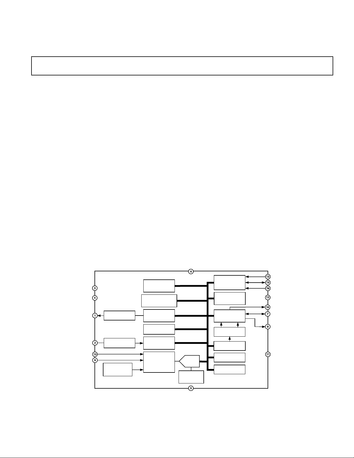
FUNCTIONAL BLOCK DIAGRAM
Monitor and PWM Fan Controller
ADM1030*
PRODUCT DESCRIPTION
The ADM1030 is an ACPI-compliant two-channel digital thermometer and under/over temperature alarm, for use in computers
and thermal management systems. Optimized for the Pentium
III, the higher 1°C accuracy offered allows systems designers to
safely reduce temperature guardbanding and increase system
performance. A Pulsewidth Modulated (PWM) Fan Control output controls the speed of a cooling fan by varying output duty
cycle. Duty cycle values between 33%–100% allow smooth
control of the fan. The speed of the fan can be monitored via a
TACH input for a fan with a tach output. The TACH input can
be programmed as an analog input, allowing the speed of a 2-wire
fan to be determined via a sense resistor. The device will also
detect a stalled fan. A dedicated Fan Speed Control Loop provides control even without the intervention of CPU software. It
also ensures that if the CPU or system locks up, the fan can still
be controlled based on temperature measurements, and the fan
speed adjusted to correct any changes in system temperature.
Fan Speed may also be controlled using existing ACPI software.
One input (two pins) is dedicated to a remote temperaturesensing diode with an accuracy of ±1°C, and a local temperature
sensor allows ambient temperature to be monitored. The device
has a programmable INT output to indicate error conditions.
There is a dedicated FAN_FAULT output to signal fan failure.
The THERM pin is a fail-safe output for over-temperature
conditions that can be used to throttle a CPU clock.
V
CC
NC
NC
PWM_OUT
TACH/AIN
D+
D–
*Patents pending.
Pentium is a registered
trademark of Intel Corporation.
ADM1030
PWM
CONTROLLER
TACH SIGNAL
CONDITIONING
BANDGAP
TEMPERATURE
SENSOR
SLAVE
ADDRESS
REGISTER
FA N
CHARACTERISTICS
REGISTER
FAN SPEED
CONFIG
REGISTER
T
MIN/TRANGE
REGISTER
FA N
SPEED
COUNTER
ANALOG
MULTIPLEXER
REV. 0
Information furnished by Analog Devices is believed to be accurate and
reliable. However, no responsibility is assumed by Analog Devices for its
use, nor for any infringements of patents or other rights of third parties
which may result from its use. No license is granted by implication or
otherwise under any patent or patent rights of Analog Devices.
SERIAL BUS
INTERFACE
ADDRESS
POINTER
REGISTER
INTERRUPT
STATUS
REGISTER
LIMIT
COMPARATOR
VALUE AND LIMIT
REGISTERS
OFFSET
ADC
2.5V
BANDGAP
REFERENCE
GND
One Technology Way, P.O. Box 9106, Norwood, MA 02062-9106, U.S.A.
Tel: 781/329-4700 www.analog.com
Fax: 781/326-8703 © Analog Devices, Inc., 2001
REGISTERS
CONFIGURATION
REGISTER
NC = NO CONNECT
ADD
SDA
SCL
NC
INT
THERM
FAN_FAULT
NC

ADM1030–SPECIFICATIONS
(TA = T
MIN
to T
, VCC = V
MAX
MIN
to V
, unless otherwise noted.)
MAX
1
Parameter Min Typ Max Unit Test Conditions/Comments
POWER SUPPLY
Supply Voltage, V
Supply Current, I
CC
CC
3.0 3.30 5.5 V
1.4 3 mA Interface Inactive, ADC Active
32 50 µA Standby Mode
TEMPERATURE-TO-DIGITAL CONVERTER
Internal Sensor Accuracy ± 1 ± 3 °C
Resolution 0.25 °C
External Diode Sensor Accuracy ± 1 °C60°C ≤ T
≤ 100°C
D
Resolution 0.125 °C
Remote Sensor Source Current 180 µA High Level
11 µA Low Level
OPEN-DRAIN DIGITAL OUTPUTS
(THERM, INT, FAN_FAULT, PWM_OUT)
Output Low Voltage, V
High-Level Output Leakage Current, I
OL
OH
0.4 V I
0.1 1 µAV
= –6.0 mA; VCC = 3 V
OUT
= VCC; VCC = 3 V
OUT
DIGITAL INPUT LEAKAGE CURRENT
Input High Current, I
Input Low Current, I
Input Capacitance, C
DIGITAL INPUT LOGIC LEVELS
IH
IL
IN
2
–1 µAV
1 µAV
5pF
IN
IN
= V
= 0
CC
(ADD, THERM, TACH)
Input High Voltage, V
Input Low Voltage, V
IL
IH
2.1 V
0.8 V
OPEN-DRAIN SERIAL DATA
BUS OUTPUT (SDA)
Output Low Voltage, V
High-Level Output Leakage Current, I
OL
OH
0.4 V I
0.1 1 µAV
= –6.0 mA; VCC = 3 V
OUT
= V
OUT
CC
SERIAL BUS DIGITAL INPUTS
(SCL, SDA)
Input High Voltage, V
Input Low Voltage, V
IL
IH
2.1 V
0.8 V
Hysteresis 500 mV
FAN RPM-TO-DIGITAL CONVERTER
Accuracy ± 6% 60°C ≤ T
≤ 100°C
A
Resolution 8 Bits
TACH Nominal Input RPM 4400 RPM Divisor N = 1, Fan Count = 153
2200 RPM Divisor N = 2, Fan Count = 153
1100 RPM Divisor N = 4, Fan Count = 153
550 RPM Divisor N = 8, Fan Count = 153
Conversion Cycle Time 637 ms
SCLK
SW
BUF
SU;STA
HD;STA
LOW
HIGH
SU;DAT
HD;DAT
3
10 100 kHz See Figure 1
50 ns See Figure 1
4.7 µs See Figure 1
4.7 µs See Figure 1
4 µs See Figure 1
SU;STO
4 µs See Figure 1
1.3 µs See Figure 1
450µs See Figure 1
R
F
1000 ns See Figure 1
300 ns See Figure 1
250 ns See Figure 1
300 ns See Figure 1
SERIAL BUS TIMING
Clock Frequency, f
Glitch Immunity, t
Bus Free Time, t
Start Setup Time, t
Start Hold Time, t
Stop Condition Setup Time t
SCL Low Time, t
SCL High Time, t
SCL, SDA Rise Time, t
SCL, SDA Fall Time, t
Data Setup Time, t
Data Hold Time, t
NOTES
1
Typicals are at TA = 25°C and represent most likely parametric norm. Shutdown current typ is measured with VCC = 3.3 V.
2
ADD is a three-state input that may be pulled high, low or left open-circuit.
3
Timing specifications are tested at logic levels of VIL = 0.8 V for a falling edge and VIH = 2.2 V for a rising edge.
Specifications subject to change without notice.
–2–
REV. 0
ADM1030
ABSOLUTE MAXIMUM RATINGS*
Positive Supply Voltage (VCC) . . . . . . . . . . . . . . . . . . . . 6.5 V
Voltage on Any Input or Output Pin . . . . . . . . –0.3 V to +6.5 V
Input Current at Any Pin . . . . . . . . . . . . . . . . . . . . . . . ± 5 mA
Package Input Current . . . . . . . . . . . . . . . . . . . . . . . ±20 mA
Maximum Junction Temperature (T
) . . . . . . . . . . 150°C
JMAX
Storage Temperature Range . . . . . . . . . . . . –65°C to +150°C
Lead Temperature, Soldering
Vapor Phase 60 sec . . . . . . . . . . . . . . . . . . . . . . . . . 215°C
Infrared 15 sec . . . . . . . . . . . . . . . . . . . . . . . . . . . . 200°C
ESD Rating All Pins . . . . . . . . . . . . . . . . . . . . . . . . . . 2000 V
*Stresses above those listed under Absolute Maximum Ratings may cause perma-
nent damage to the device. This is a stress rating only; functional operation of the
device at these or any other conditions above those indicated in the operational
section of this specification is not implied. Exposure to absolute maximum rating
conditions for extended periods may affect device reliability.
THERMAL CHARACTERISTICS
16-Lead QSOP Package
θJA = 105°C/W, θJC = 39°C/W
t
HIGH
t
F
t
SU:DAT
SCL
t
HD:STA
t
LOW
t
R
t
HD:DAT
ORDERING GUIDE
Temperature Package Package
Model Range Description Option
ADM1030ARQ 0°C to 100°C 16-Lead QSOP RQ-16
t
HD:STA
t
SU:STA
t
SU:STO
SDA
t
BUF
S
PSP
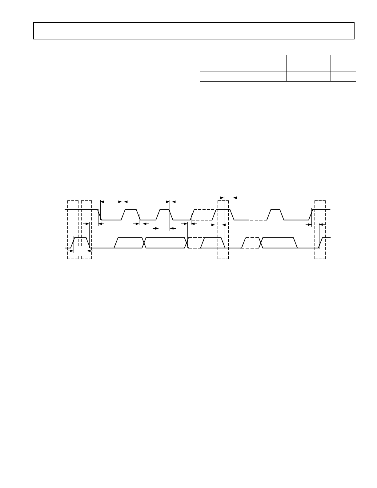
Figure 1. Diagram for Serial Bus Timing
REV. 0
–3–

ADM1030
PIN FUNCTION DESCRIPTIONS
Pin No. Mnemonic Description
1 PWM_OUT Digital Output (Open-Drain). Pulsewidth modulated output to control fan speed. Requires pull-
up resistor (10 kΩ typical).
2 TACH/AIN Digital/Analog Input. Fan tachometer input to measure fan speed. May be reprogrammed as an
analog input to measure speed of a 2-wire fan via a sense resistor (2 Ω typical)
3, 4, 11, 12 NC Not Connected.
5 GND System Ground.
6V
CC
7 THERM Digital I/O (Open-Drain). An active low thermal overload output that indicates a violation of a
8 FAN_FAULT Digital Output (Open-Drain). Can be used to signal a fan failure. Requires pull-up resistor
9 D– Analog Input. Connected to cathode of an external temperature-sensing diode. The temperature-
10 D+ Analog Input. Connected to anode of the external temperature-sensing diode.
13 ADD Three-state Logic Input. Sets two lower bits of device SMBus address.
14 INT Digital Output (Open-Drain). Can be programmed as an interrupt output for temperature/fan
15 SDA Digital I/O. Serial Bus Bidirectional Data. Open-drain output. Requires pull-up resistor
16 SCL Digital Input. Serial Bus Clock. Requires pull-up resistor (2.2 kΩ typ).
Power. Can be powered by 3.3 V Standby power if monitoring in low power states is required.
temperature set point (overtemperature). Also acts as an input to provide external fan control.
When this pin is pulled low by an external signal, a status bit is set, and the fan speed is set to
full-on. Requires pull-up resistor (10 kΩ).
(typically 10 kΩ).
sensing element is either a Pentium III substrate transistor or a general-purpose 2N3904.
speed interrupts. Requires pull-up resistor (10 kΩ typical).
(2.2 kΩ typical).
PIN CONFIGURATION
NC
NC
GND
V
THERM
CC
1
2
3
ADM1030
4
TOP VIEW
5
(Not to Scale)
6
7
8
NC = NO CONNECT
PWM_OUT
TACH/AIN
FAN_FAULT
16
SCL
SDA
15
INT
14
ADD
13
NC
12
NC
11
10
D+
D–
9
–4–
REV. 0
Typical Performance Characteristics–ADM1030
DXP – DXN CAPACITANCE – nF
–2
–10
1472.2
REMOTE TEMPERATURE ERROR – ⴗC
3.3
4.7
10 22
–3
–5
–7
–9
–6
1
–11
–12
–13
–14
–15
–16
0
–1
–4
–8
15
10
5
0
–5
–10
–15
REMOTE TEMPERATURE ERROR – ⴗC
–20
1
3.3
LEAKAGE RESISTANCE – M⍀
DXP TO GND
DXP TO VCC (3.3V)
10 30
100
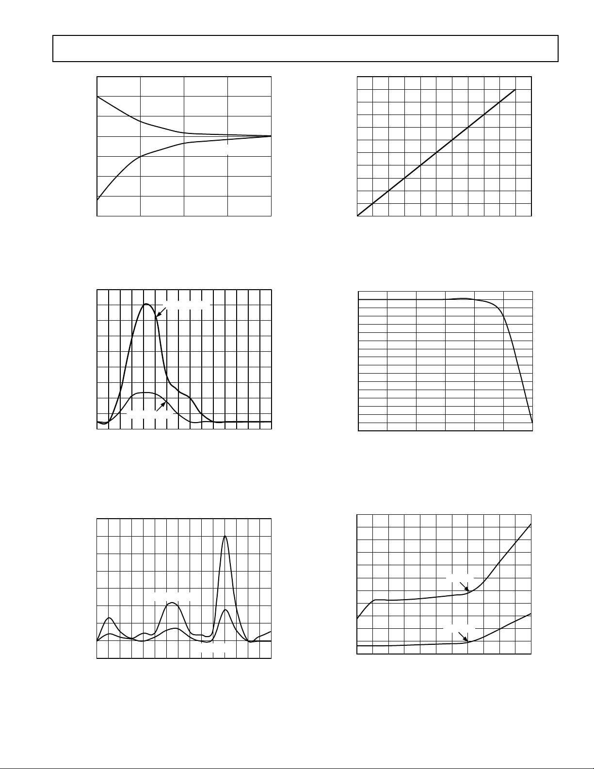
TPC 1. Temperature Error vs. PCB Track Resistance
17
15
13
11
9
7
5
3
REMOTE TEMPERATURE ERROR – ⴗC
1
–1
0
VIN = 200mV p-p
500k 2M
VIN = 100mV p-p
4M 6M 10M 100M 400M
FREQUENCY – Hz
110
100
90
80
70
60
50
READING – ⴗC
40
30
20
10
0
06010
20
40 50
30
PIII TEMPERATURE – ⴗC
70 80 90 100 110
TPC 4. Pentium III Temperature Measurement vs.
ADM1030 Reading
TPC 2. Temperature Error vs. Power Supply Noise
Frequency
7
6
C
ⴗ
5
4
3
2
1
REMOTE TEMPERATURE ERROR –
0
–1
0 400M100k 1M
VIN = 40mV p-p
200M 300M
100M
FREQUENCY – Hz
VIN = 20mV p-p
500M
TPC 3. Temperature Error vs. Common-Mode Noise
Frequency
REV. 0
TPC 5. Temperature Error vs. Capacitance between
D+ and D–
110
100
90
80
70
60
50
40
SUPPLY CURRENT – A
30
20
10
0
0751
5
25 50
10
SCLK FREQUENCY – kHz
VCC = 5V
VCC = 3.3V
100 250 500 750 1000
TPC 6. Standby Current vs. Clock Frequency
–5–
ADM1030
7
6
5
4
3
2
1
REMOTE TEMPERATURE ERROR – ⴗC
0
–1
0 400M100k
VIN = 30mV p-p
VIN = 20mV p-p
1M
100M
FREQUENCY – Hz
200M 300M
500M
C
ⴗ
ERROR –
0.08
–0.08
–0.16
–0.24
–0.32
–0.40
–0.48
–0.56
–0.64
–0.72
–0.80
0
0
20 40 60 80 85 100 105 120
TEMPERATURE – ⴗC
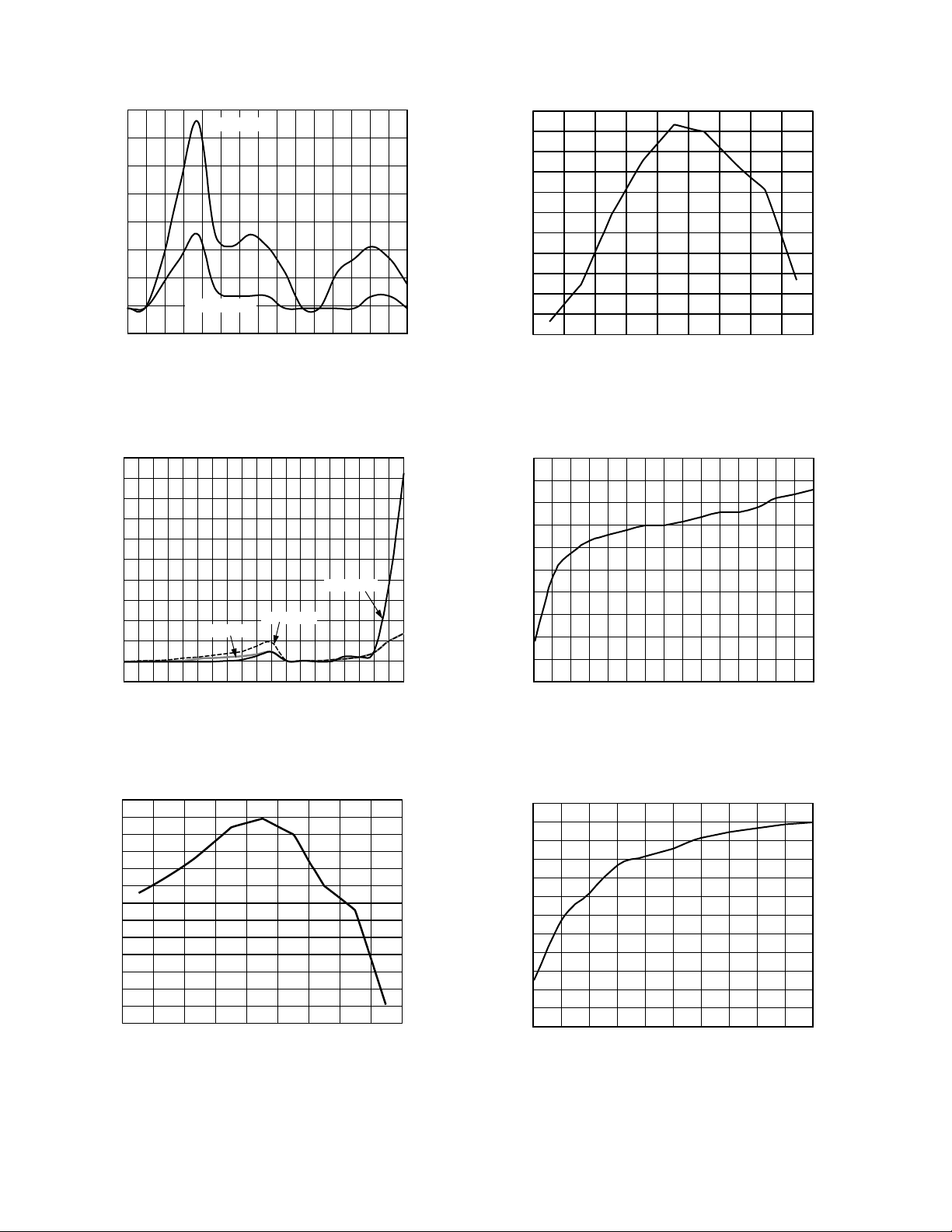
TPC 7. Temperature Error vs. Differential-Mode Noise
Frequency
200
180
160
140
120
100
80
60
SUPPLY CURRENT – A
40
20
0
–20
0 1.1 1.3 1.5 1.7 1.9 2.1
ADD = V
CC
SUPPLY VOLTAGE – V
ADD = GND
ADD = Hi-Z
2.9 4.5
2.5
TPC 8. Standby Supply Current vs. Supply Voltage
0.16
0.08
0
–0.08
–0.16
–0.24
C
ⴗ
–0.32
–0.40
ERROR –
–0.48
–0.56
–0.64
–0.72
–0.80
–0.88
20 40 60 80 85 100 105 120
0
TEMPERATURE – ⴗC
TPC 10. Remote Sensor Error
1.30
1.25
1.20
1.15
1.10
1.05
1.00
0.95
SUPPLY CURRENT – mA
0.90
0.85
0.80
2.0
2.8 3.2 3.6 4.0 4.4 4.82.2 2.6 3.0 3.4 3.8 4.2 4.6 5.0
2.4
SUPPLY VOLTAGE – V
TPC 11. Supply Current vs. Supply Voltage
120
110
100
90
80
70
60
50
40
TEMPERATURE – ⴗC
30
20
10
0
0
2
4681013579
TIME – Sec
TPC 9. Local Sensor Error
–6–
TPC 12. Response to Thermal Shock
REV. 0

ADM1030
GENERAL DESCRIPTION
The ADM1030 is a temperature monitor and PWM fan controller for microprocessor-based systems. The device communicates
with the system via a serial System Management Bus. The serial
bus controller has a hardwired address pin for device selection
(Pin 13), a serial data line for reading and writing addresses and
data (Pin 15), and an input line for the serial clock (Pin 16). All
control and programming functions of the ADM1030 are performed over the serial bus. The device also supports the SMBus
Alert Response Address (ARA) function.
INTERNAL REGISTERS OF THE ADM1030
A brief description of the ADM1030’s principal internal registers is given below. More detailed information on the function of
each register is given in Table XII to Table XXVI.
Configuration Register
Provides control and configuration of various functions on
the device.
Address Pointer Register
This register contains the address that selects one of the other
internal registers. When writing to the ADM1030, the first byte
of data is always a register address, which is written to the
Address Pointer Register.
Status Registers
These registers provide status of each limit comparison.
Value and Limit Registers
The results of temperature and fan speed measurements are
stored in these registers, along with their limit values.
Fan Speed Config Register
This register is used to program the PWM duty cycle for the fan.
Offset Registers
Allows the temperature channel readings to be offset by a 5-bit
two’s complement value written to these registers. These values
will automatically be added to the temperature values (or subtracted from if negative). This allows the systems designer to
optimize the system if required, by adding or subtracting up to
15°C from a temperature reading.
Fan Characteristics Register
This register is used to select the spin-up time, PWM frequency,
and speed range for the fan used.
THERM Limit Registers
These registers contain the temperature values at which THERM
will be asserted.
T
MIN/TRANGE
Registers
These registers are read/write registers that hold the minimum
temperature value below which the fan will not run when the
device is in Automatic Fan Speed Control Mode. These registers also hold the values defining the range over that auto fan
control will be provided, and hence determines the temperature
at which the fan will run at full speed.
SERIAL BUS INTERFACE
Control of the ADM1030 is carried out via the SMBus. The
ADM1030 is connected to this bus as a slave device, under the
control of a master device, e.g., the 810 chipset.
The ADM1030 has a 7-bit serial bus address. When the device
is powered up, it will do so with a default serial bus address.
The five MSBs of the address are set to 01011, the two LSBs
are determined by the logical state of Pin 13 (ADD). This is a
REV. 0
–7–
three-state input that can be grounded, connected to V
CC
, or
left open-circuit to give three different addresses. The state of
the ADD pin is only sampled at power-up, so changing ADD
with power on will have no effect until the device is powered off,
then on again.
Table I. ADD Pin Truth Table
ADD Pin A1 A0
GND 0 0
No Connect 1 0
V
CC
01
If ADD is left open-circuit, the default address will be 0101110.
The facility to make hardwired changes at the ADD pin allows
the user to avoid conflicts with other devices sharing the same
serial bus, for example, if more than one ADM1030 is used in
a system.
The serial bus protocol operates as follows:
1. The master initiates data transfer by establishing a START
condition, defined as a high-to-low transition on the serial
data line SDA while the serial clock line SCL remains high.
This indicates that an address/data stream will follow. All
slave peripherals connected to the serial bus respond to the
START condition, and shift in the next 8 bits, consisting of a
7-bit address (MSB first) plus an R/W bit that determines the
direction of the data transfer, i.e., whether data will be
written to or read from the slave device.
The peripheral whose address corresponds to the transmitted
address responds by pulling the data line low during the low
period before the ninth clock pulse, known as the Acknowledge Bit. All other devices on the bus now remain idle while
the selected device waits for data to be read from or written
to it. If the R/W bit is a 0, the master will write to the slave
device. If the R/W bit is a 1, the master will read from the
slave device.
2. Data is sent over the serial bus in sequences of nine clock
pulses, eight bits of data followed by an Acknowledge Bit
from the slave device. Transitions on the data line must
occur during the low period of the clock signal and remain
stable during the high period, as a low-to-high transition
when the clock is high may be interpreted as a STOP signal.
The number of data bytes that can be transmitted over the
serial bus in a single READ or WRITE operation is limited
only by what the master and slave devices can handle.
3. When all data bytes have been read or written, stop condi-
tions are established. In WRITE mode, the master will pull
the data line high during the tenth clock pulse to assert a
STOP condition. In READ mode, the master device will
override the acknowledge bit by pulling the data line high
during the low period before the ninth clock pulse. This is
known as No Acknowledge. The master will then take the
data line low during the low period before the tenth clock
pulse, then high during the tenth clock pulse to assert a
STOP condition.
Any number of bytes of data may be transferred over the serial
bus in one operation, but it is not possible to mix read and write
in one operation, because the type of operation is determined at
the beginning and cannot subsequently be changed without
starting a new operation.
ADM1030
In the case of the ADM1030, write operations contain either
one or two bytes, and read operations contain one byte, and
perform the following functions.
To write data to one of the device data registers or read data
from it, the Address Pointer Register must be set so that the
correct data register is addressed; data can then be written into
that register or read from it. The first byte of a write operation
always contains an address that is stored in the Address Pointer
Register. If data is to be written to the device, then the write
operation contains a second data byte that is written to the
register selected by the address pointer register.
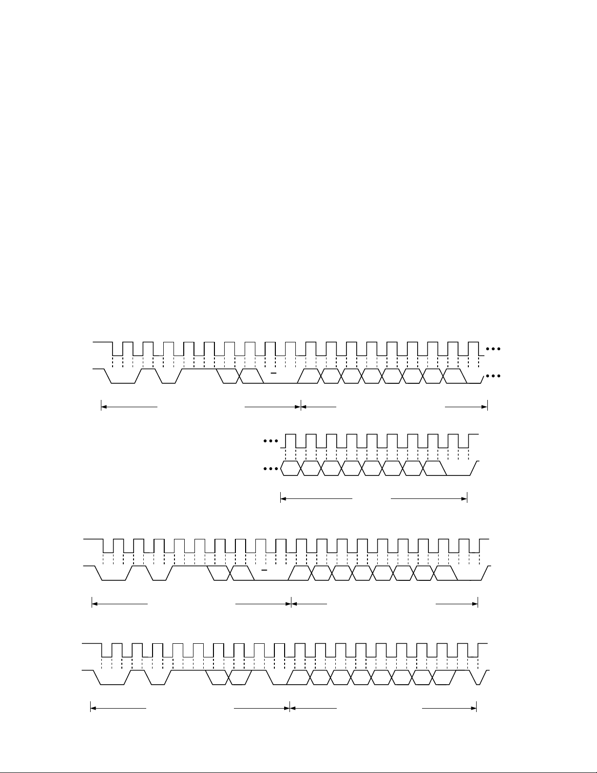
This is illustrated in Figure 2a. The device address is sent over
the bus followed by R/W set to 0. This is followed by two data
bytes. The first data byte is the address of the internal data
register to be written to, which is stored in the Address Pointer
Register. The second data byte is the data to be written to the
internal data register.
When reading data from a register there are two possibilities:
1. If the ADM1030’s Address Pointer Register value is unknown
or not the desired value, it is first necessary to set it to the
correct value before data can be read from the desired data
register. This is done by performing a write to the ADM1030
19
SCL
as before, but only the data byte containing the register address
is sent, as data is not to be written to the register. This is
shown in Figure 2b.
A read operation is then performed consisting of the serial bus
address, R/W bit set to 1, followed by the data byte read from
the data register. This is shown in Figure 2c.
2. If the Address Pointer Register is known to be already at the
desired address, data can be read from the corresponding
data register without first writing to the Address Pointer
Register, so Figure 2b can be omitted.
NOTES
1. Although it is possible to read a data byte from a data register
without first writing to the Address Pointer Register, if the
Address Pointer Register is already at the correct value, it is
not possible to write data to a register without writing to the
Address Pointer Register, because the first data byte of a
write is always written to the Address Pointer Register.
2. In Figures 2a to 2c, the serial bus address is shown as the
default value 01011(A1)(A0), where A1 and A0 are set by
the three-state ADD pin.
3. The ADM1030 also supports the Read Byte protocol, as
described in the System Management Bus specification.
1
9
SDA
START BY
MASTER
0
1011
SERIAL BUS ADDRESS BYTE
FRAME 1
SCL (CONTINUED)
SDA (CONTINUED)
A0
A1
R/W
ACK. BY
ADM1030
1
D7
D7
D6
D6
ADDRESS POINTER REGISTER BYTE
D5
D5
D4
FRAME 3
DATA BYTE
D4
FRAME 2
D3
D2
D3
D2
D1
D1
D0
D0
9
ACK. BY
ADM1030
ACK. BY
ADM1030
STOP BY
MASTER
Figure 2a. Writing a Register Address to the Address Pointer Register, then Writing Data to the Selected Register
D0
9
ACK. BY
ADM1030
STOP BY
MASTER
SCL
SDA
START BY
MASTER
19
0
1011
FRAME 1
SERIAL BUS ADDRESS BYTE
A0
A1
R/W
ADM1030
ACK. BY
1
D6
D7
ADDRESS POINTER REGISTER BYTE
D5
D4
FRAME 2
D3
D2
D1
Figure 2b. Writing to the Address Pointer Register Only
9
SCL
19
1
SDA
START BY
MASTER
0
1011
SERIAL BUS ADDRESS BYTE
FRAME 1
A0
A1
R/W
ACK. BY
ADM1030
D6
D7
D4
D5
FRAME 2
DATA BYTE FROM ADM1030
D3
D2
Figure 2c. Reading Data from a Previously Selected Register
–8–
D1
D0
NO ACK.
BY MASTER
STOP BY
MASTER
REV. 0
ADM1030
ALERT RESPONSE ADDRESS
Alert Response Address (ARA) is a feature of SMBus devices
that allows an interrupting device to identify itself to the host
when multiple devices exist on the same bus.
The INT output can be used as an interrupt output or can be used
as an SMBALERT. One or more INT outputs can be connected
to a common SMBALERT line connected to the master. If a
device’s INT line goes low, the following procedure occurs:
1. SMBALERT pulled low.
2. Master initiates a read operation and sends the Alert
Response Address (ARA = 0001 100). This is a general call
address that must not be used as a specific device address.
3. The device whose INT output is low responds to the Alert
Response Address, and the master reads its device address.
The address of the device is now known and can be interrogated in the usual way.
4. If more than one device’s INT output is low, the one with
the lowest device address will have priority, in accordance
with normal SMBus arbitration.
5. Once the ADM1030 has responded to the Alert Response
Address, it will reset its INT output; however, if the error
condition that caused the interrupt persists, INT will be
reasserted on the next monitoring cycle.
TEMPERATURE MEASUREMENT SYSTEM
Internal Temperature Measurement
The ADM1030 contains an on-chip bandgap temperature sensor. The on-chip ADC performs conversions on the output of
this sensor and outputs the temperature data in 10-bit two’s
complement format. The resolution of the local temperature
sensor is 0.25°C. The format of the temperature data is shown
in Table II.
External Temperature Measurement
The ADM1030 can measure the temperature of an external
diode sensor or diode-connected transistor, connected to Pins
9 and 10.
These pins are a dedicated temperature input channel. The
function of Pin 7 is as a THERM input/output and is used to
flag overtemperature conditions.
The forward voltage of a diode or diode-connected transistor,
operated at a constant current, exhibits a negative temperature
coefficient of about –2 mV/°C. Unfortunately, the absolute
value of V
, varies from device to device, and individual
BE
calibration is required to null this out, so the technique is
unsuitable for mass production.
The technique used in the ADM1030 is to measure the change
in V
when the device is operated at two different currents.
BE
This is given by:
∆V
= KT/q × ln (N)
BE
where:
K is Boltzmann’s constant.
q is charge on the carrier.
T is absolute temperature in Kelvins.
N is ratio of the two currents.
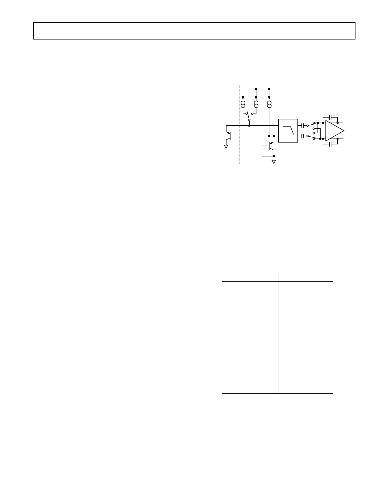
Figure 3 shows the input signal conditioning used to measure
the output of an external temperature sensor. This figure shows
the external sensor as a substrate transistor, provided for temperature monitoring on some microprocessors, but it could equally
well be a discrete transistor.
V
DD
REMOTE
SENSING
TRANSISTOR
IN ⴛ II
D+
D–
BIAS
DIODE
BIAS
LOW-PASS
f
FILTER
= 65kHz
C
V
V
OUT+
OUT–
TO
ADC
Figure 3. Signal Conditioning
If a discrete transistor is used, the collector will not be grounded,
and should be linked to the base. If a PNP transistor is used, the
base is connected to the D– input and the emitter to the D+
input. If an NPN transistor is used, the emitter is connected to
the D– input and the base to the D+ input.
One LSB of the ADC corresponds to 0.125°C, so the ADM1030
can theoretically measure temperatures from –127°C to +127.75°C,
although –127°C is outside the operating range for the device.
The extended temperature resolution data format is shown in
Tables III and IV.
Table II. Temperature Data Format (Local Temperature and
Remote Temperature High Bytes)
Temperature (ⴗC) Digital Output
–128°C 1000 0000
–125°C 1000 0011
–100°C 1001 1100
–75°C 1011 0101
–50°C 1100 1110
–25°C 1110 0111
–1°C 1111 1111
0°C 0000 0000
+1°C 0000 0001
+10°C 0000 1010
+25°C 0001 1001
+50°C 0011 0010
+75°C 0100 1011
+100°C 0110 0100
+125°C 0111 1101
+127°C 0111 1111
REV. 0
–9–
 Loading...