

Dual PWM Fan Controller and Temperature
a
FEATURES
Software Programmable and Automatic Fan Speed
Control
Automatic Fan Speed Control Allows Control
Independent of CPU Intervention after Initial Setup
Control Loop Minimizes Acoustic Noise and Power
Consumption
Remote and Local Temperature Monitoring
Dual Fan Speed Measurement
Supports Backup and Redundant Fans
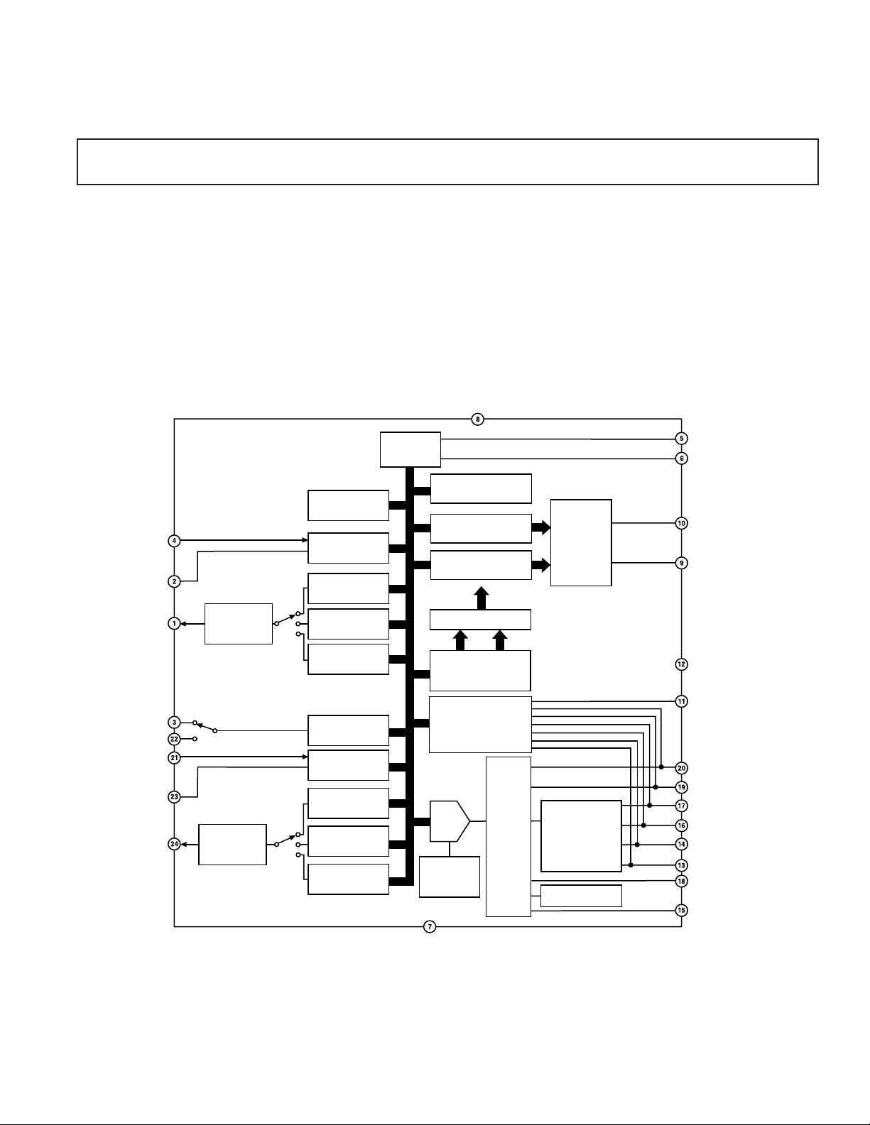
FUNCTIONAL BLOCK DIAGRAM
ADM1029
SLAVE ADDRESS
REGISTER
PRESENT1
FAULT1
FAN 1 STATUS
REGISTER
FAN 1 MIN
SPEED REGISTER
Monitor for High Availability Systems
ADM1029*
Supports Hot Swapping of Fans
Cascadable Fault Output Allows Fault Signaling
between Multiple ADM1029s
Address Pin Allows Up to Eight ADM1029s in A System
Small 24-Lead QSOP Package
APPLICATIONS
Network Servers and Personal Computers
Microprocessor-Based Office Equipment
High Availability Telecommunications Equipment
V
CC
SERIAL BUS
INTERFACE
ADDRESS POINTER
REGISTER
INTERRUPT MASK
REGISTERS
INTERRUPT STATUS
REGISTERS
INTERRUPT
MASKING
SCL
SDA
INT
CFAULT
DRIVE1
TACH1
TACH2
PRESENT2
FAULT2
DRIVE2
*Protected by U.S. Patent Numbers 6,255,973 and 6,188,189
PWM
CONTROLLER
PWM
CONTROLLER
FAN 1 ALARM
SPEED REGISTER
FAN 1 HOT-PLUG
SPEED REGISTER
FAN SPEED
COUNTER
FAN 2 STATUS
REGISTER
FAN 2 MIN
SPEED REGISTER
FAN 2 ALARM
SPEED REGISTER
FAN 2 HOT-PLUG
SPEED REGISTER
REFERENCE
GND
REV. A
Information furnished by Analog Devices is believed to be accurate and
reliable. However, no responsibility is assumed by Analog Devices for its
use, nor for any infringements of patents or other rights of third parties that
may result from its use. No license is granted by implication or otherwise
under any patent or patent rights of Analog Devices. Trademarks and
registered trademarks are the property of their respective companies.
LIMIT COMPARATOR
VALUE AND LIMIT
REGISTERS
G.P. I/O REGISTER
ADC
ANALOG
MUX
BANDGAP
One Technology Way, P.O. Box 9106, Norwood, MA 02062-9106, U.S.A.
Tel: 781/329-4700 www.analog.com
Fax: 781/326-8703 © 2003 Analog Devices, Inc. All rights reserved.
REMOTE SENSOR
SIGNAL
CONDITIONING
BANDGAP
TEMP SENSOR
RESET
GPIO2
AIN1/GPIO1
AIN0/GPIO0
D2+/GPIO6
D2–/GPIO5
D1+/GPIO4
D1–/GPIO3
TMIN/INSTALL
ADD

1, 2
ADM1029–SPECIFICATIONS
(TA = T
Parameter Min Typ Max Unit Test Conditions/Comments
POWER SUPPLY
Supply Voltage, V
Supply Current, I
CC
CC
3.0 3.30 5.5 V
TEMPERATURE-TO-DIGITAL CONVERTER
Internal Sensor Accuracy ± 1 ± 3 °C
Resolution 1 °C
External Diode Sensor Accuracy ± 3 ± 5 °C0°C ≤ T
Resolution 1 °C
Remote Sensor Source Current 90 µA High Level
ANALOG-TO-DIGITAL CONVERTER
Total Unadjusted Error, TUE ± 1%Note 3
Differential Nonlinearity, DNL ± 1 LSB
Power Supply Sensitivity ± 1 %/ V
Conversion Time
Analog Input or Internal Temperature 11.6 ms
External Temperature 185.6 ms
FAN RPM-TO-DIGITAL CONVERTER
Accuracy ± 6%60°C ≤ TA ≤ 100°C: VCC = 3.3 V
Full-Scale Count 255
FAN 1 and FAN 2 Nominal Input RPM
4
Internal Clock Frequency 56.4 60.0 63.6 kHz
OPEN-DRAIN DIGITAL OUTPUTS (INT, CFAULT)
Output Low Voltage, V
High Level Output Current, I
OL
OH
OPEN-DRAIN SERIAL DATA BUS OUTPUT (SDA)
Output Low Voltage, V
High Level Output Leakage Current, I
OL
OH
SERIAL BUS DIGITAL INPUTS (SCL, SDA)
Input High Voltage, V
Input Low Voltage, V
IL
IH
2.1 V
Hysteresis 500 mV
DIGITAL INPUT LOGIC LEVELS RESET,
GPIO1-6, FAULT1/2, TACH1/2, PRESENT1/2
Input High Voltage, V
Input Low Voltage, V
IL
IH
2.1 V
DIGITAL INPUT CURRENT
Input High Current, I
Input Low Current, I
Input Capacitance, C
SERIAL BUS TIMING
Clock Frequency, f
Glitch Immunity, t
Bus Free Time, t
Start Setup Time, t
Start Hold Time, t
IH
IL
IN
5
SCLK
SW
BUF
SU:STA
HD:STA
Stop Condition Setup Time, t
SU:STO
–1 µAV
10 100 kHz See Figure 1
4.7 µs See Figure 1
4.7 µs See Figure 1
4 µs See Figure 1
4 µs See Figure 1
to T
MIN
, VCC = V
MAX
MIN
to V
, unless otherwise noted.)
MAX
1.7 3.0 mA Interface Inactive, ADC Active
1.5 mA ADC Inactive, DAC Active
10 60 µA Shutdown Mode
≤ 100°C
A
5.5 µA Low Level
8800 rpm Divisor = 1, Fan Count = 153
4400 rpm Divisor = 2, Fan Count = 153
2200 rpm Divisor = 4, Fan Count = 153
1100 rpm Divisor = 8, Fan Count = 153
0.4 V I
0.1 1 µAV
0.4 V I
0.1 1 µAV
= –6.0 mA, VCC = 3 V
OUT
= V
OUT
OUT
OUT
CC
= –6.0 mA, VCC = 3 V
= V
CC
0.8 V
0.8 V
= V
IN
+1 µAV
IN
CC
= 0
20 pF
50 ns See Figure 1
–2–
REV. A
ADM1029
Parameter Min Typ Max Unit Test Conditions/Comments
5
SERIAL BUS TIMING
SCL Low Time, t
SCL High Time, t
SCL, SDA Rise Time, t
SCL, SDA Fall Time, t
Data Setup Time, t
Data Hold Time, t
NOTES
1
All voltages are measured with respect to GND, unless otherwise specified.
2
Typicals are at TA = 25°C and represent most likely parametric norm. Shutdown current typ is measured with VCC = 3.3 V.
3
TUE (Total Unadjusted Error) includes Offset, Gain, and Linearity errors of the ADC, multiplexer.
4
The total fan count is based on two pulses per revolution of the fan tachometer output.
5
Timing specifications are tested at logic levels of VIL = 0.8 V for a falling edge and VIH = 2.1 V for a rising edge.
Specifications subject to change without notice.
(continued)
LOW
HIGH
SU:DAT
HD:DAT
1.3 µs See Figure 1
450µs See Figure 1
R
F
1000 ns See Figure 1
300 ns See Figure 1
250 ns See Figure 1
300 ns See Figure 1
ABSOLUTE MAXIMUM RATINGS*
Positive Supply Voltage (VCC) . . . . . . . . . . . . . . . . . . . . . 6.5 V
Voltage on Pins 13–18 . . . . . . . . . . . . –0.3 V to (V
+ 0.3 V)
CC
Voltage on Any Other Input or Output Pin . . . . –0.3 V to +6.5 V
Input Current at Any Pin . . . . . . . . . . . . . . . . . . . . . . . ± 5 mA
Package Input Current . . . . . . . . . . . . . . . . . . . . . . . ± 20 mA
Maximum Junction Temperature (T
max) . . . . . . . . . . 150°C
J
Storage Temperature Range . . . . . . . . . . . . –65°C to +150°C
Lead Temperature
Vapor Phase (60 sec) . . . . . . . . . . . . . . . . . . . . . . . . . 215°C
Infrared (15 sec) . . . . . . . . . . . . . . . . . . . . . . . . . . . . 200°C
ESD Rating All Pins . . . . . . . . . . . . . . . . . . . . . . . . . . . 2000 V
*Stresses above those listed under Absolute Maximum Ratings may cause perma-
nent damage to the device. This is a stress rating only; functional operation of the
device at these or any other conditions above those indicated in the operational
section of this specification is not implied. Exposure to absolute maximum rating
conditions for extended periods may affect device reliability.
THERMAL CHARACTERISTICS
24-Lead QSOP Package:
θ
= 105°C/W, θJC = 39°C/W
JA
ORDERING GUIDE
Temperature Package Package
Model Range Description Option
ADM1029ARQ 0°C to 100°C Shrink Small Outline RQ-24
Package (QSOP)
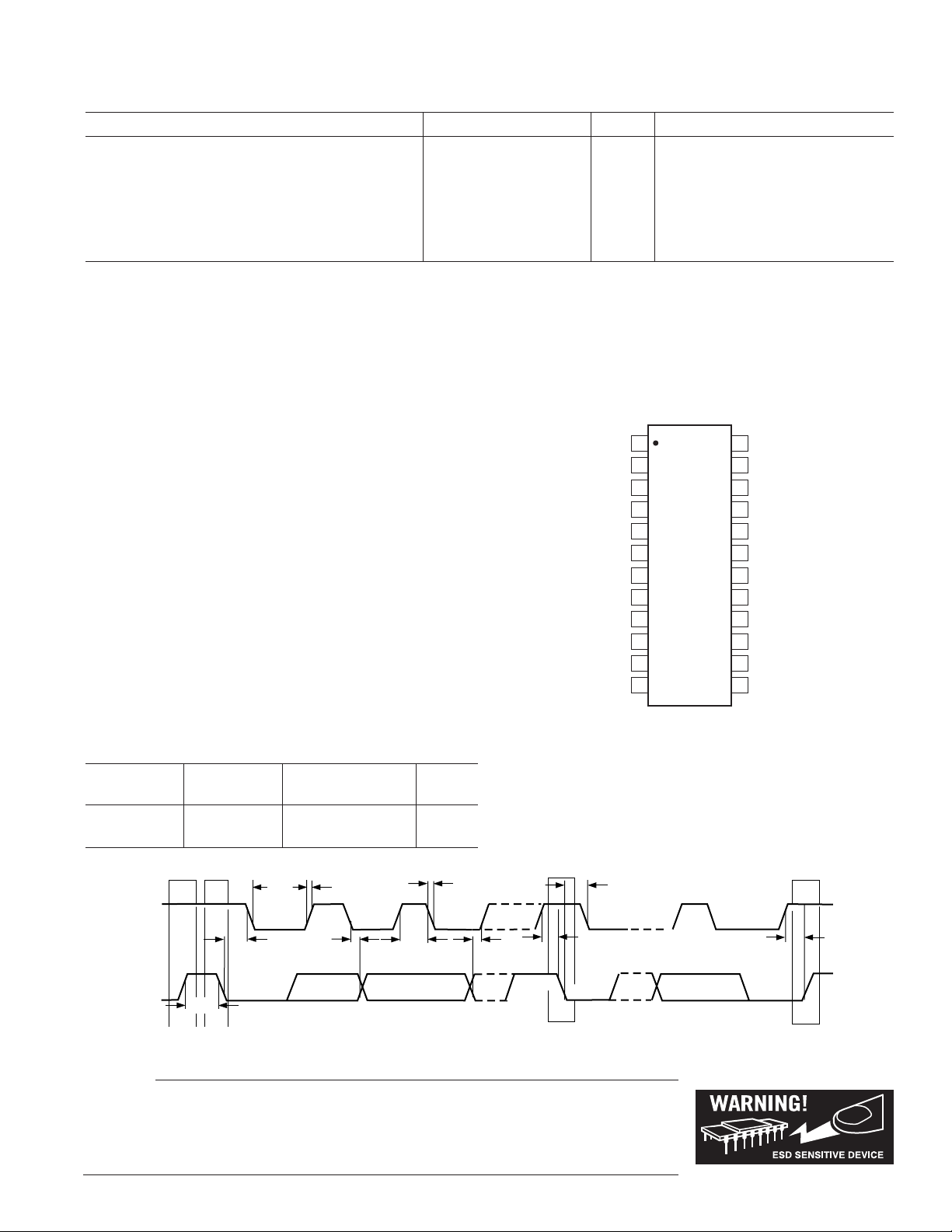
PIN CONFIGURATION
1
DRIVE1
2
FAULT1
3
TACH1
SCL
SDA
GND
V
INT
GPIO2
RESET
CC
4
5
6
7
(Not To Scale)
8
9
10
11
12
ADM1029
TOP VIEW
PRESENT1
CFAULT
24
DRIVE2
23
FAULT2
22
TACH2
21
PRESENT2
20
AIN1/GPIO1
19
AIN0/GPIO0
18
TMIN/INSTALL
17
D2+/GPIO6
16
D2–/GPIO5
15
ADD
14
D1+/GPIO4
13
D2–/GPIO3
SCL
SDA
t
R
t
LOW
t
HD;STA
t
BUF
S
P
t
HD;DAT
t
HIGH
t
F
t
SU;DAT
t
HD;STA
t
SU;STA
S
Figure 1. Diagram for Serial Bus Timing
CAUTION
ESD (electrostatic discharge) sensitive device. Electrostatic charges as high as 4000 V readily
accumulate on the human body and test equipment and can discharge without detection. Although the
ADM1029 features proprietary ESD protection circuitry, permanent damage may occur on devices
subjected to high energy electrostatic discharges. Therefore, proper ESD precautions are recommended
to avoid performance degradation or loss of functionality.
REV. A
–3–
t
SU;STO
P

ADM1029
PIN FUNCTION DESCRIPTIONS
Pin No. Mnemonic Description
1 DRIVE1 Open Drain Digital Output. Pulsewidth Modulated (PWM) output to control the speed of
Fan 1. Requires 10 kΩ typical pull-up resistor.
2 FAULT1 Open Drain Digital I/O. When used with a fan having a fault output, a Logic 0 input to this pin
signals a fault on Fan 1. Also used as a fault output.
3 TACH1 Open Drain Digital Input. Digital fan tachometer input for Fan 1. Will accept logic signals up
to 5 V even when V
4 PRESENT1
Open Drain Digital Input. A shorting link in the fan connector holds this pin low when
Fan 1 is connected.
5 SCL Open Drain Digital Input. Serial Bus Clock. Requires 2.2 kΩ pull-up typical.
6 SDA Digital I/O. Serial Bus bidirectional data. Open-drain output requires 2.2 kΩ pull-up.
7GND System Ground
8V
CC
Power (3.0 V to 5.5 V). Typically powered from 3.3 V power rail. Bypass with the parallel
combination of 10 µF (electrolytic or tantalum) and 0.1 µF (ceramic) bypass capacitors.
9 CFAULT
Open Drain Digital I/O. Cascade fault input/output used for fault signaling between
multiple ADM1029s.
10 INT Digital Output. Interrupt Request (Open Drain). The output is enabled when Bit 1 of the
Configuration Register is set to 0. The default state is enabled.
11 GPIO2 Open Drain Digital I/O. General-purpose logic I/O pin.
12 RESET Open Drain Digital Input. Active low reset input.
13 D1–/GPIO3 Analog Input/Open Drain Digital I/O. Connected to cathode of external temperature-sensing
diode, or may be reconfigured as a general-purpose logic input/output.
14 D1+/GPIO4 Analog Input/Open Drain Digital I/O. Connected to anode of external temperature-sensing
diode, or may be reconfigured as a general-purpose logic input/output.
15 ADD Eight-Level Analog Input. Used to set the three LSBs of the serial bus address.
16 D2–/GPIO5 Analog Input/Open Drain Digital I/O. Connected to cathode of external temperature-sensing
diode, or may be reconfigured as a general-purpose logic input/output.
17 D2+/GPIO6 Analog Input/Open Drain Digital I/O. Connected to anode of external temperature-sensing
diode, or may be reconfigured as a general-purpose logic input/output.
18 TMIN/INSTALL Eight-Level Analog Input. The voltage on this pin defines whether automatic fan speed control
is enabled, the minimum temperature at which the fan(s) will turn on in automatic speed con-
trol mode, and the number of fans that should be installed.
19 AIN0/GPIO0 Analog Input/Open Drain Digital I/O. May be configured as a 0 V to 2.5 V analog input or as a
general-purpose digital I/O pin.
20 AIN1/GPIO1 Analog Input/Open Drain Digital I/O. May be configured as a 0 V to 2.5 V analog input or as a
general-purpose digital I/O pin.
21 PRESENT2 Open Drain Digital Input. A shorting link in the fan connector holds this pin low when Fan 2
is connected.
22 TACH2 Open Drain Digital Input. Digital fan tachometer input for Fan 2. Will accept logic signals up
to 5 V even when V
23 FAULT2 Open Drain Digital I/O. When used with a fan having a fault output, a Logic 0 input to this pin
signals a fault on Fan 2. Also used as a fault output.
24 DRIVE2 Open Drain Digital Output. Pulsewidth Modulated (PWM) output to control the speed of
Fan 2. Requires 10 kΩ typical pull-up resistor.
is lower than 5 V.
CC
is lower than 5 V.
CC
–4–
REV. A
Typical Performance Characteristics–ADM1029
110
100
90
80
70
60
50
40
30
20
10
0
0 10 20 30 40 50 60 70 80 90 100 110
READING
MEASURED TEMPERATURE
1
0
–1
–2
–3
–4
–5
–6
–7
–8
–9
–10
–11
–12
–13
–14
–15
–16
1.0 2.2 3.3 4.7 10.0 22.0 47.0
REMOTE TEMPERATURE ERROR – ⴗC
DXP – DXN CAPACITANCE – nF
15
10
5
0
–5
–10
–15
REMOTE TEMPERATURE ERROR – ⴗC
–20
0 3.3 10 30 100
LEAKAGE RESISTANCE – M⍀
DXP TO GND
DXP TO VCC(3.3V)
TPC 1. Remote Temperature Error vs. PC Board Track
Resistance
4.5
4.0
3.5
3.0
2.5
2.0
1.5
1.0
0.5
0
REMOTE TEMPERATURE ERROR – ⴗC
V
IN
–0.5
–1.0
01481216 20 50 100 200 300
VIN = 250mV p-p
= 100mV p-p
FREQUENCY – MHz
400
500
600
TPC 2. Remote Temperature Error vs. Power Supply
Noise Frequency
TPC 4. Pentium® III Temperature Measurement vs.
ADM1029 Reading
TPC 5. Remote Temperature Error vs. Capacitance
Between D+ and D–
10
9
8
7
6
5
4
3
REV. A
2
1
REMOTE TEMPERATURE ERROR – ⴗC
0
–1
00.40.810 600150 40050 250 500100 200 350 450 550300
FREQUENCY – MHz
TPC 3. Remote Temperature Error vs. Common-Mode
Noise Frequency
V
= 100mV p-p
IN
V
= 60mV p-p
IN
VIN = 40mV p-p
–5–
80
70
60
50
40
30
SUPPLY CURRENT – A
20
10
0
0 1 5 10 25 50 75 100 250 500 750 1000
SCLK FREQUENCY – kHz
VCC = 5V
VCC = 3.3V
TPC 6. Standby Current vs. Clock Frequency
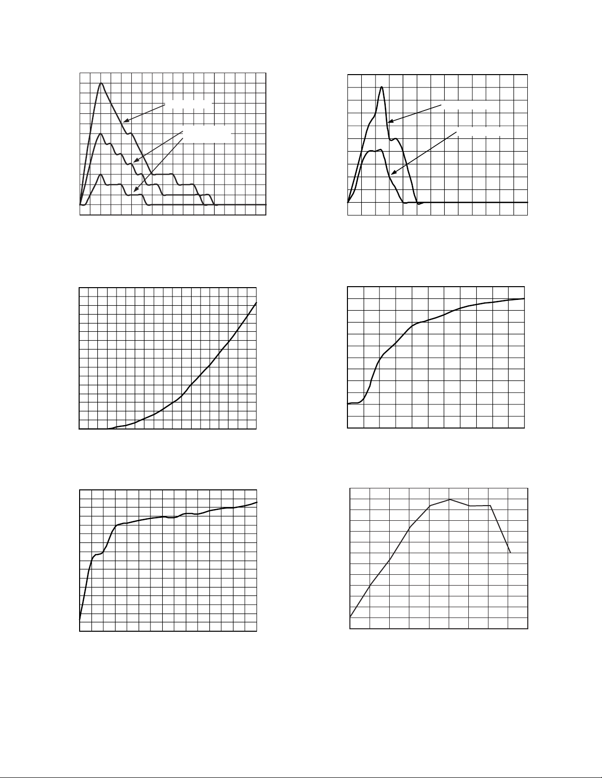
ADM1029
13
12
11
10
9
8
7
6
5
4
3
2
1
REMOTE TEMPERATURE ERROR – ⴗC
0
–1
0
12 40020 300100 500148 16 50 200
VIN = 40mV p-p
VIN = 30mV p-p
V
IN
FREQUENCY – MHz
= 20mV p-p
600
TPC 7. Remote Temperature Error vs. Differential-Mode
Noise Frequency
32
30
28
26
24
22
20
18
16
14
12
10
SUPPLY CURRENT – A
8
6
4
2
0
1.0 1.4 1.8 2.2 2.6 3.0 3.4 3.8 4.2 4.6
SUPPLY VOLTAGE – V
TPC 8. Standby Supply Current vs. Supply Voltage
10
9
8
7
6
5
4
3
2
1
LOCAL TEMPERATURE ERROR – ⴗC
0
–1
0 1 4 8 12 16 20 50 100 200 300 400 500 600
FREQUENCY – MHz
VIN = 250mV p-p
VIN = 100mV p-p
TPC 10. Local Sensor Temperature Error vs. Power Supply
Noise Frequency
120
110
100
90
80
70
60
50
40
TEMPERATURE – ⴗC
30
20
10
0
0 1 2 3 4 5 6 7 8 9 10
TIME – Seconds
TPC 11. ADM1029 Response to Thermal Shock
1.80
1.75
1.70
1.65
1.60
1.55
1.50
1.45
1.40
1.35
1.30
1.25
SUPPLY CURRENT – mA
1.20
1.15
1.10
1.05
1.00
2.0 2.2 2.4 2.6 2.8 3.0 3.2 3.4 3.6 3.8 4.0 4.2 4.4 4.6 4.8 5.0
SUPPLY VOLTAGE – V
TPC 9. Supply Current vs. Supply Voltage
–6–
0.10
0.00
–0.10
–0.20
–0.30
–0.40
–0.50
–0.60
ERROR – ⴗC
–0.70
–0.80
–0.90
–1.00
–1.10
–1.20
02040608085100 105 120
TEMPERATURE – ⴗC
TPC 12. Remote Temperature Error
REV. A
ADM1029
0.05
0.00
–0.05
–0.10
–0.15
–0.20
–0.25
–0.30
ERROR – ⴗC
–0.35
–0.40
–0.45
–0.50
–0.55
–0.60
02040608085100 105 120
TEMPERATURE – ⴗC
TPC 13. Local Temperature Error
PRODUCT DESCRIPTION
The ADM1029 is a versatile fan controller and monitor for use
in personal computers, servers, telecommunications equipment,
or any high-availability system where reliable control and monitoring of multiple cooling fans is required. Each ADM1029 can
control the speed of one or two fans and can measure the speed
of fans that have a tachometer output. The ADM1029 can also
measure the temperature of one or two external sensing diodes
or an internal temperature sensor, allowing fan speed to be
adjusted to keep system temperature within acceptable limits. The
ADM1029 has FAULT inputs for use with fans that can signal
failure conditions, and inputs to detect whether or not fans are
connected.
The ADM1029 communicates with the host processor over an
System Management (SMBus) serial bus. It supports eight
different serial bus addresses, so that up to eight devices can
be connected to a common bus, controlling up to sixteen fans.
This makes software support and hardware design scalable.
The ADM1029 has an interrupt output (INT) that allows it
to signal fault conditions to the host processor. It also has a
separate, cascadable fault output (CFAULT) that allows the
ADM1029 to signal a fault condition to other ADM1029s.
The ADM1029 has a number of useful features including an
automatic fan speed control option implemented in hardware
with no software requirement, automatic use of backup fans in
the event of fan failure, and supports hot-swapping of failed fans.
Table I. Resistor Ratios for Setting Serial Bus Address
FUNCTIONAL DESCRIPTION
SERIAL BUS INTERFACE
Control of the ADM1029 is carried out via the serial bus. The
ADM1029 is connected to this bus as a slave device, under the
control of a master device.
The ADM1029 has a 7-bit serial bus address. The four MSBs of
the address are set to 0101. The three LSBs can be set by the
user to give a total of eight different addresses, allowing up to
eight ADM1029s to be connected to a single serial bus segment.
To minimize device pin count and size, the three LSBs are set
using a single pin (ADD, Pin 15). This is an 8-level input whose
input voltage is set by a potential divider. The voltage on ADD
is sampled immediately after power-up and digitized by the
on-chip ADC to determine the value of the 3 LSBs. Since ADD
is sampled only at power-up, any changes made while power is
on will have no effect.
V
CC
R1
ADD
R2
GND
ADM1029
Figure 2. Setting the Serial Address
Table I shows resistor values for setting the 3 LSBs of the serial
bus address. The same principle is used to set the voltage on Pin
18 (TMIN/INSTALL), which controls the automatic fan speed
control function, and also tells the ADM1029 how many fans
should be installed, as described later.
If several ADM1029s are used in a system, their ADD inputs
can tap off a single potential divider, as shown in Figure 3.
V
CC
ADDRESS XXXX111
1.5k⍀
ADDRESS XXXX110
1k⍀
ADDRESS XXXX101
1k⍀
ADDRESS XXXX100
1k⍀
ADDRESS XXXX011
1k⍀
ADDRESS XXXX010
1k⍀
ADDRESS XXXX001
1.5k⍀
ADDRESS XXXX000
GND
ADD
ADD
ADD
ADD
ADD
ADD
ADD
ADD
ADM1029 #1
ADM1029 #2
ADM1029 #3
ADM1029 #4
ADM1029 #5
ADM1029 #6
ADM1029 #7
ADM1029 #8
Figure 3. Setting Address of up to Eight ADM1029s
3 MSBs Ideal Ratio R1 R2 Actual Error
of ADC R2/(R1 + R2) (k⍀)(k⍀) R2/(R1 + R2) % Address
111 N/A 0 ∞ 100101111
110 0.8125 18 82 0.82 +0.75 0101110
101 0.6875 22 47 0.6812 –0.63 0101101
100 0.5625 12 15 0.5556 –0.69 0101100
011 0.4375 15 12 0.4444 +0.69 0101011
010 0.3125 47 22 0.3188 +0.63 0101010
001 0.1875 82 18 0.18 –0.75 0101001
000 N/A ∞ 00 00101000
REV. A
–7–
ADM1029
The serial bus protocol operates as follows:
1. The master initiates data transfer by establishing a START
condition, defined as a high-to-low transition on the serial
data line SDA, while the serial clock line SCL remains high.
This indicates that an address/data stream will follow. All
slave peripherals connected to the serial bus respond to the
START condition, and shift in the next eight bits, consisting
of a 7-bit address (MSB first) plus an R/W bit, which determines the direction of the data transfer, i.e., whether data
will be written to or read from the slave device.
The peripheral whose address corresponds to the transmitted
address responds by pulling the data line low during the low
period before the ninth clock pulse, known as the Acknowledge Bit. All other devices on the bus now remain idle while
the selected device waits for data to be read from or written
to it. If the R/W bit is a 0, the master will write to the slave
device. If the R/W bit is a 1 the master will read from the
slave device.
2. Data is sent over the serial bus in sequences of nine clock
pulses, eight bits of data followed by an acknowledge bit
from the slave device. Transitions on the data line must
191
SCL
occur during the low period of the clock signal and remain
stable during the high period, as a low-to-high transition
when the clock is high may be interpreted as a STOP signal.
The number of data bytes that can be transmitted over the
serial bus in a single READ or WRITE operation is limited
only by what the master and slave devices can handle.
3. When all data bytes have been read or written, stop conditions are established. In WRITE mode, the master will pull
the data line high during the tenth clock pulse to assert a
STOP condition. In READ mode, the master device will
override the acknowledge bit by pulling the data line high
during the low period before the ninth clock pulse. This is
known as No Acknowledge. The master will then take the
data line low during the low period before the tenth clock
pulse, high during the tenth clock pulse to assert a STOP
condition.
Any number of bytes of data may be transferred over the serial
bus in one operation, but it is not possible to mix read and write
in one operation, because the type of operation is determined at
the beginning and cannot subsequently be changed without
starting a new operation.
9
SDA
START BY
MASTER
101A2
0
SERIAL BUS ADDRESS BYTE
FRAME 1
SCL (CONTINUED)
SDA (CONTINUED)
A0
A1
W
R/
ACK. BY
ADM1029
1
D7 D6 D5
D6
D7
ADDRESS POINTER REGISTER BYTE
D4 D3 D2 D1
D5
FRAME 2
D4 D3 D2 D1
FRAME 3
DATA BYTE
D0
ACK. BY
ADM1029
D0
ACK. BY
ADM1029
9
STOP BY
MASTER
Figure 4a. Writing a Register Address to the Address Pointer Register, then Writing Data to the Selected Register
SCL
SDA
START BY
MASTER
191
101A2
0
SERIAL BUS ADDRESS BYTE
FRAME 1
A0 D7
A1
R/W
ACK. BY
ADM1029
D6
ADDRESS POINTER REGISTER BYTE
D4 D3 D2 D1
D5
FRAME 2
D0
ACK. BY
ADM1029
9
STOP BY
MASTER
Figure 4b. Writing to the Address Pointer Register Only
191
SCL
9
SDA
START BY
MASTER
101A2
0
SERIAL BUS ADDRESS BYTE
D6 D5
D4 D3 D2 D1
DATA BYTE FROM ADM1029
FRAME 2
FRAME 1
A0 D7
A1
R/W
ACK. BY
ADM1029
Figure 4c. Reading Data from a Previously Selected Register
–8–
D0
NO ACK.
BY MASTER
STOP BY
MASTER
REV. A

ADM1029
In the case of the ADM1029, write operations contain either
one or two bytes, and read operations contain one byte, and
perform the following functions:
To write data to one of the device data registers or read data
from it, the Address Pointer Register must be set so that the
correct data register is addressed, data can be written into that
register or read from it. The first byte of a write operation always
contains an address that is stored in the Address Pointer Register. If data is to be written to the device, the write operation
contains a second data byte that is written to the register
selected by the address pointer register.
This is illustrated in Figure 4a. The device address is sent over
the bus followed by R/W set to 0. This is followed by two data
bytes. The first data byte is the address of the internal data
register to be written to, which is stored in the Address Pointer
Register. The second data byte is the data to be written to the
internal data register.
When reading data from a register there are two possibilities:
1. If the ADM1029’s Address Pointer Register value is unknown
or not the desired value, it is first necessary to set it to the
correct value before data can be read from the desired data
register. This is done by performing a write to the ADM1029
as before, but only the data byte containing the register address
is sent, as data is not to be written to the register. This is
shown in Figure 4b.
A read operation is then performed consisting of the serial
bus address, R/W bit set to 1, followed by the data byte read
from the data register. This is shown in Figure 4c.
2. If the Address Pointer Register is known to be already at the
desired address, data can be read from the corresponding
data register without first writing to the Address Pointer
Register, so Figure 4b can be omitted.
Note: although it is possible to read a data byte from a data
register without first writing to the Address Pointer Register,
if the Address Pointer Register is already at the correct value,
it is not possible to write data to a register without writing to
the Address Pointer Register, because the first data byte of a
write is always written to the Address Pointer Register.
ALERT RESPONSE ADDRESS
The ADM1029 has an interrupt (INT) output that is asserted
low when a fault condition occurs. Several INT outputs can be
wire OR’d to a common interrupt line. When the host processor
receives an interrupt request, it would normally need to read the
interrupt status register of each device to identify which device
had made the interrupt request. However, the ADM1029 supports the optional Alert Response Address function of the SMBus
protocol. When the host processor receives an interrupt request
it can send a general call address (0001100) over the bus. The
device asserting INT will then send its own slave address back
to the host processor, so the device asserting INT can be identified immediately.
If more than one device is asserting INT, all devices will try to
respond with their slave address, but an arbitration process
ensures that only the lowest address will be received by the host.
After sending its slave address, the first device will then clear its
INT output. The host can then check if the INT is still low and
send the general call again if necessary until all devices asserting
INT have responded.
The ARA function can be disabled by setting Bit 2 of the Configuration Register (address 01h).
TEMPERATURE MEASUREMENT SYSTEM
LOCAL TEMPERATURE MEASUREMENT
The ADM1029 contains an on-chip bandgap temperature sensor,
whose output is digitized by the on-chip ADC. The temperature
data is stored in the Local Temp Value Register (address A0h).
As both positive and negative temperatures can be measured, the
temperature data is stored in two’s complement format, as shown
in Table II. Theoretically, the temperature sensor and ADC can
measure temperatures from –128°C to +127°C with a resolution
of 1°C, but temperatures outside the operating temperature
range of the device cannot be measured by the internal sensor.
REMOTE TEMPERATURE MEASUREMENT
The ADM1029 can measure the temperature of one or two
remote diode-connected transistors, connected to Pins 13 and
14 and/or 16 and 17. The data from the temperature measurements is stored in the Remote 1 and Remote 2 Temp Value
Registers (addresses A1h and A2h).
If two remote temperature measurements are not required, Pins
16 and 17 can be reconfigured as general-purpose logic I/O
pins, as explained later.
The forward voltage of a diode or diode-connected transistor,
operated at a constant current, exhibits a negative temperature
coefficient of about –2 mV/°C. The absolute value of V
varies
BE
from device to device and individual calibration is required to
null this out so, unfortunately, the technique is unsuitable for
mass production.
The technique used in the ADM1029 is to measure the change
in V
when the device is operated at two different currents.
BE
This is given by:
∆V
= KT/q × ln(N)
BE
where:
K is Boltzmann’s constant
q is charge on the carrier
T is absolute temperature in Kelvins
N is ratio of the two currents
Figure 5 shows the input signal conditioning used to measure
the output of a remote temperature sensor. This figure shows
the external sensor as a substrate transistor, provided for temperature monitoring on some microprocessors, but it could equally
well be a discrete transistor.
If a discrete transistor is used, the collector will not be grounded,
and should be linked to the base. If a PNP transistor is used, the
base is connected to the D– input and the emitter to the D+
input. If an NPN transistor is used, the emitter is connected to
the D– input and the base to the D+ input.
REV. A
–9–
ADM1029
V
DD
I
N ⴛ I
REMOTE
SENSING
TRANSISTOR
I
D+
D–
BIAS
DIODE
BIAS
LOW-PASS FILTER
f
C
= 65kHz
Figure 5. Signal Conditioning for Remote Diode Temperature Sensors
V
OUT
TO ADC
V
OUT
+
–
To prevent ground noise interfering with the measurement, the
more negative terminal of the sensor is not referenced to ground,
but biased above ground by an internal diode at the D– input. If
the sensor is used in a noisy environment, a capacitor of value
up to 1000 pF may be placed between the D+/D– pins.
To measure ∆V
, the sensor is switched between operating currents
BE
of I and N × I. The resulting waveform is passed through a 65 kHz
low-pass filter to remove noise, and to a chopper-stabilized amplifier
that performs the functions of amplification and rectification of
the waveform to produce a dc voltage proportional to ∆VBE. This
voltage is measured by the ADC to give a temperature output in
8-bit two’s complement format. To further reduce the effects of
noise, digital filtering is performed by averaging the results of 16
measurement cycles. An external temperature measurement takes
nominally 9.6 ms.
The results of external temperature measurements are stored in
8-bit, two’s complement format, as illustrated in Table II.
OFFSET REGISTERS
Digital noise and other error sources can cause offset errors in
the temperature measurement, particularly on the remote sensors. The ADM1029 offers a way to minimize these effects. The
offsets on the three temperature channels can be measured during
system characterization and stored as two’s complement values
in three offset registers at addresses 30h to 32h. The offset
values are automatically added to, or subtracted from, the temperature values, depending on whether the two’s complement
number corresponds to a positive or negative offset. Offset values from –15°C to +15°C are allowed.
The default value in the offset registers is zero, so if no offsets
are programmed, the temperature measurements are unaltered.
TEMPERATURE LIMITS
The contents of the Local and Remote Temperature Value Registers (addresses A0h to A2h) are compared to the contents of the
High and Low Limit Registers at addresses 90h to 92h and 98h
to 9Ah. How the ADM1029 responds to overtemperature/
undertemperature conditions depends on the status of the Temperature Fault Action Registers (addresses 40h to 42h). The
response of CFAULT, INT, and fan-speed-to-temperature events
depends on the setting of these registers, as explained later.
Table II. Temperature Data Format
Temperature Digital Output
–128°C 1000 0000
–125°C 1000 0011
–100°C 1001 1100
–75°C 1011 0101
–50°C 1100 1110
–25°C 1110 0111
0°C 0000 0000
+10°C 0000 1010
+25°C 0001 1001
+50°C 0011 0010
+75°C 0100 1011
+100°C 0110 0100
+125°C 0111 1101
+127°C 0111 1111
–10–
REV. A

ADM1029
LAYOUT CONSIDERATIONS
Digital boards can be electrically noisy environments, and care
must be taken to protect the analog inputs from noise, particularly when measuring the very small voltages from a remote diode
sensor. The following precautions should be taken:
1. Place the ADM1029 as close as possible to the remote sens-
ing diode. Provided that the worst noise sources such as
clock generators, data/address buses, and CRTs are avoided,
this distance can be 4 to 8 inches.
2. Route the D+ and D– tracks close together, in parallel, with
grounded guard tracks on each side. Provide a ground plane
under the tracks if possible.
3. Use wide tracks to minimize inductance and reduce noise
pickup. Ten mil track minimum width and spacing is
recommended.
GND
D+
D–
GND
10MIL
10MIL
10MIL
10MIL
10MIL
10MIL
10MIL
Figure 6. Arrangement of Signal Tracks
4. Try to minimize the number of copper/solder joints, which
can cause thermocouple effects. Where copper/solder joints
are used, make sure that they are in both the D+ and D–
path and at the same temperature.
Thermocouple effects should not be a major problem as 1°C
corresponds to about 240 µV, and thermocouple voltages are
about 3 µV/
o
C of temperature difference. Unless there are two
thermocouples with a big temperature differential between
them, thermocouple voltages should be much less than 200 µV.
5. Place 0.1 µF bypass and 1000 pF input filter capacitors close
to the ADM1029.
6. If the distance to the remote sensor is more than 8 inches,
the use of twisted pair cable is recommended. This will work
up to about 6 to 12 feet.
7. For really long distances (up to 100 feet), use shielded
twisted pair such as Belden #8451 microphone cable. Connect the twisted pair to D+ and D– and the shield to GND
close to the ADM1029. Leave the remote end of the shield
unconnected to avoid ground loops.
Because the measurement technique uses switched current
sources, excessive cable and/or filter capacitance can affect the
measurement. When using long cables, the filter capacitor may
be reduced or removed.
Cable resistance can also introduce errors. 1 Ω series resistance
introduces about 0.5°C error.
TEMPERATURE-RELATED REGISTERS
Table III is a list of registers on the ADM1029 that are specific
to temperature measurement and control.
Table III. Temperature-Specific Registers
Address Description
0x06 Temp Devices Installed
0x30 Local Temp Offset
0x31 Remote 1 Temp Offset
0x32 Remote 2 Temp Offset
0x40 Local Temp Fault Action
0x41 Remote 1 Temp Fault Action
0x42 Remote 2 Temp Fault Action
0x48 Local Temp Cooling Action
0x49 Remote 1 Temp Cooling Action
0x4A Remote 2 Temp Cooling Action
0x80 Local Temp TMIN
0x81 Remote 1 Temp TMIN
0x82 Remote 2 Temp TMIN
0x88 Local Temp TRANGE/THYST
0x89 Remote 1 Temp TRANGE/THYST
0x8A Remote 2 Temp TRANGE/THYST
0x90 Local Temp High Limit
0x91 Remote 1 Temp High Limit
0x92 Remote 2 Temp High Limit
0x98 Local Temp Low Limit
0x99 Remote 1 Temp Low Limit
0x9A Remote 2 Temp Low Limit
0xA0 Local Temp Value
0xA1 Remote 1 Temp Value
0xA2 Remote 2 Temp Value
The flowchart in Figure 7 shows how to configure the ADM1029
to measure temperature. It also shows how to configure the
ADM1029’s behavior for out-of-limit temperature measurements.
FAN INTERFACING
The ADM1029 can be interfaced to many types of fan. It can be
used to control the speed of a simple two-wire fan. It can measure the speed of a fan with a tach output, and it can accept a
logic input from fans with a FAULT output. By means of a
shorting link in the fan connector it can also determine if a fan is
present or not and if fans have been hot-swapped.
The ADM1029 can control or monitor one or two fans. Bits 0
and 1 of the Fans Supported In System Register (03h) tell the
ADM1029 how many fans it should be controlling/monitoring.
In the following descriptions “installed” means that the corresponding bit of register 03h is set and the ADM1029 expects to
see a fan interfaced to it. It does not necessarily mean that the
fan is actually, physically, connected.
If a fan is installed, events such as a fault output and hot-swapping
of the fan can cause INT and CFAULT to be asserted, unless
they are masked for that particular event. If a fan is not installed,
but is still physically connected to the ADM1029, these events will
be ignored with respect to asserting INT or CFAULT, but will
still be reflected in the corresponding Fan Status Register.
Setting Bit 0 indicates that Fan 1 is installed and is set to 1
at power-up by default. Setting Bit 1 indicates that Fan 2 is
installed and depends on the state of Pin 18 (TMIN/INSTALL)
at power-up.
REV. A
–11–
ADM1029
DEFAULTS
LOCAL = 60ⴗC
REMOTE 1 = 70ⴗC
REMOTE 2 = 70ⴗC
DEFAULTS
LOCAL = 80ⴗC
REMOTE 1 = 100ⴗC
REMOTE 2 = 100ⴗC
DEFAULTS
LOCAL = 0ⴗC
REMOTE 1 = 0ⴗC
REMOTE 2 = 0ⴗC
CONFIGURE
TEMPERATURE LOW
LIMITS
LOCAL (REG 0x98)
REMOTE 1 (REG 0x99)
REMOTE 2 (REG 0x9A)
CONFIGURE
TEMPERATURE HIGH
LIMITS
LOCAL (REG 0x90)
REMOTE 1 (REG 0x91)
REMOTE 2 (REG 0x92)
CONFIGURE
TEMPERATURE FAULT
ACTION
LOCAL (REG 0x40)
REMOTE 1 (REG 0x41)
REMOTE 2 (REG 0x42)
CONFIGURE
TEMPERATURE COOLING
ACTION
LOCAL (REG 0x48)
REMOTE 1 (REG 0x49)
REMOTE 2 (REG 0x4A)
CONFIGURE
TEMPERATURE OFFSETS
LOCAL (REG 0x30)
REMOTE 1 (REG 0x31)
REMOTE 2 (REG 0x32)
BIT 0 = 1 ASSERT CFAULT ON OVER-TEMPERATURE
BIT 1 = 1 RUN FAN(S) ALARM SPEED ON OVER-TEMPERATURE
BIT 2 = 1 ASSERT INT ON OVER-TEMPERATURE
BIT 3 = 0 ALARM BELOW LOW TEMP LIMIT
BIT 3 = 1 ALARM ABOVE LOW TEMP LIMIT
BIT 4 = 1 ASSERT CFAULT WHEN LOW TEMP LIMIT CROSSED
BIT 5 = 1 RUN FAN ALARM SPEED ON UNDER-TEMPERATURE
BIT 6 = 1 ASSERT INT ON UNDER-TEMPERATURE
BIT 7 LATCHES A TEMPERATURE OUT-OF-LIMIT EVENT
7 6 5 4 3 2 1 0
IS
TEMPERATURE
>
HIGH LIMIT?
YES
IS
TEMPERATURE
>
HIGH LIMIT?
YES
ALARM ABOVE OR
BELOW LOW TEMP
LIMIT?
0 = ALARM BELOW TEMP LIMIT
IS
TEMPERATURE
>
HIGH LIMIT?
YES
CFAULT
FANS RUN
ALARM SPEED
INT
MEASURE
TEMPERATURE
LOCAL (REG 0xA0)
REMOTE 1 (REG 0xA1)
REMOTE 2 (REG 0xA2)
LOW TEMP LIMIT
LOW TEMP LIMIT
CROSSED?
YES
AUTOMATIC FAN SPEED CONTROL (SEE TABLE XI LATER)
BIT 0 = 1 FAN 1 RUNS AT ALARM SPEED FOR OUT-OF-LIMIT TEMPERATURE EVENTS;
BIT 1 = 1 FAN 2 RUNS AT ALARM SPEED FOR OUT-OF-LIMIT TEMPERATURE EVENTS;
XXXXXX10
OTHERWISE, FAN 1 RUNS AT SPEED DETERMINED BY AUTOMATIC FAN
CONTROL.
OTHERWISE, FAN 2 RUNS AT SPEED DETERMINED BY AUTOMATIC FAN
CONTROL.
LOW TEMP LIMIT
CROSSED?
YES
CROSSED?
1 = ALARM ABOVE TEMP LIMIT
CFAULT
YES
FANS RUN ALARM SPEED
INT
Figure 7. Temperature Sensing Flowchart
–12–
REV. A
ADM1029
If two fans are installed, Bit 0 would be 1 by default and Pin
18 would be tied high* to set Bit 1. If only one fan is installed, it
would normally be Fan 1 and Pin 18 would be tied low* to
clear Bit 1. However, both of these bits can be modified by
writing to the register, so it is possible to have Fan 2 installed
and not Fan 1, or even have no fans installed.
*Note that Pin 18 also sets TMIN for automatic fan speed control. If this function
is used, Pin 18 would be set to some other level according to Table IX.
FAULT INPUTS/OUTPUTS
The ADM1029 can be used with fans that have a fault output
which indicates if the fan has stalled or failed. If one or both of
the FAULT inputs (Pin 2 or Pin 23) goes low, both INT and
CFAULT will be asserted.
Events on the fault inputs are also reflected in Bits 2 and 3 of the
corresponding Fan Status Registers at addresses 10h and 11h.
Bit 2 reflects the inverse state of the FAULT pin (0 if FAULT is
high, 1 if FAULT is low), while Bit 3 is latched high if a FAULT
input goes low. It must be cleared by writing a zero to it.
If the fan(s) being used do not have a FAULT output, the FAULT
input(s) on the ADM1029 should be pulled high to V
CC
.
The FAULT pins can also be configured as open-drain outputs
by setting Bit 5 of the corresponding Fan Fault Action Register
(18h or 19h). If a FAULT pin is configured as an output, it will
still function as an input. This means that when a fault input
occurs it will be latched low by the fault output, even if the fault
input is removed. The fault output can be used to drive a fan
failure indicator such as an LED.
If the FAULT pin is used as an output, any input to the FAULT
pin should also be open-drain. This will avoid the fault input
trying to source a high current into the FAULT pin if the fault
input goes high while the fault output is low.
FAN PRESENT INPUTS
The fan PRESENT signal is implemented by a shorting link
to ground in the fan connector. When the fan is plugged in,
the corresponding PRESENT input (Pin 4 or Pin 21) on the
ADM1029 is pulled low. If the fan is unplugged, the PRESENT
input will be pulled high. INT and CFAULT will be asserted
(unless masked) and the event will be reflected in Bits 0 and
Bit 1 of the corresponding Fan Status Register.
Appearance or disappearance of a PRESENT input signal during normal operation signals to the ADM1029 that a fan has
been hot-plugged or unplugged. INT and CFAULT will be
asserted (unless masked). When a fan is hot-plugged, Bit 7 of
the corresponding Fan Status Register will be set and a Fan
Free Wheel Test commences automatically.
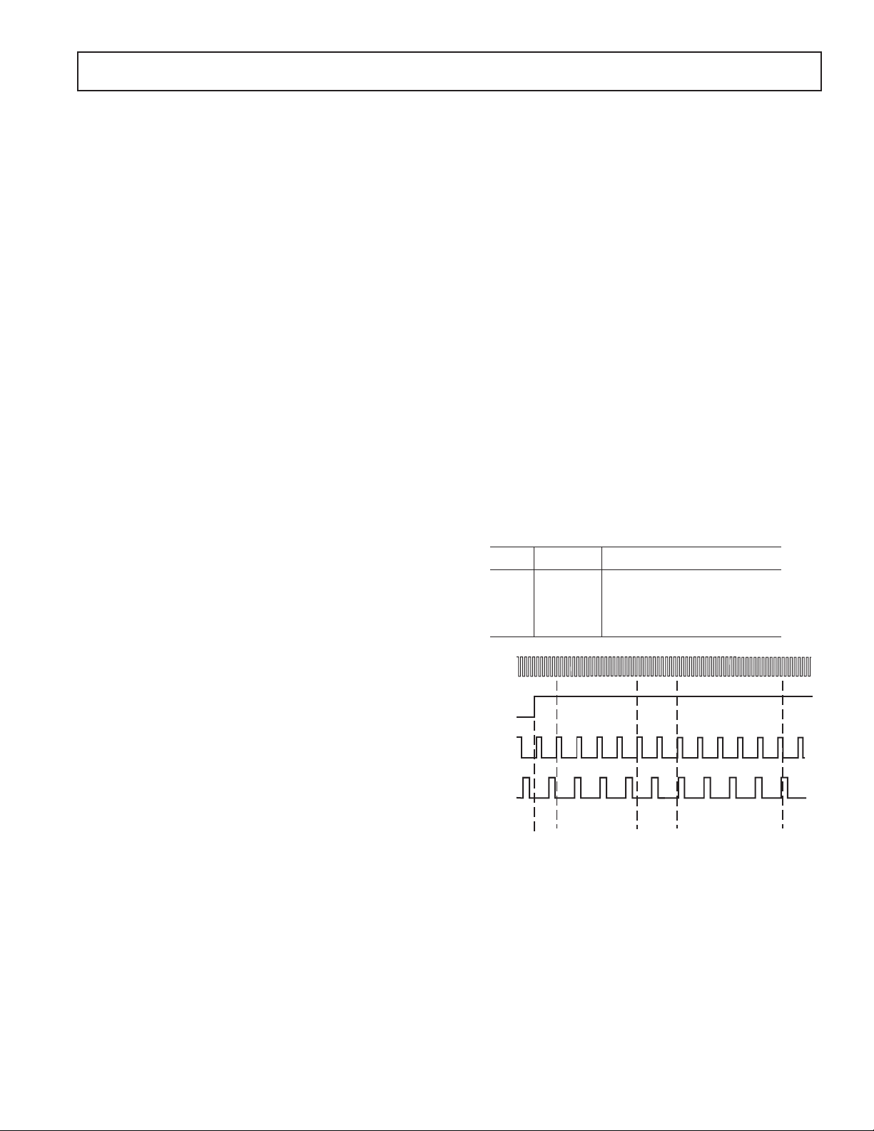
FAN SPEED MEASUREMENT
The fan counter does not count the fan tach output pulses
directly, because at low fan speeds it would take several seconds
to accumulate a reasonably large and accurate count. Instead,
the period of the fan revolution is measured by gating an onchip oscillator into the input of an 8-bit counter.
The fan speed measuring circuit is initialized on the first rising
edge of a fan tach pulse after monitoring is enabled by setting
Bit 4 of the Configuration Register. It then starts counting on
the rising edge of the second tach pulse and counts for four fan
tach periods, until the rising edge of the sixth tach pulse, or
until the counter overranges if the fan tach period is too long.
After the speed of the first fan has been measured, the speed of
the second fan (if installed) will be measured in the same way.
The measurement cycle will repeat until monitoring is disabled.
The fan speed measurements are stored in the Fan Tach Value
registers at addresses 70h and 71h.
If both fans are installed, Fan 1 will be measured first. If only
one fan is installed, the ADM1029 will still try to measure
both fans, starting with Fan 1, but the measurement on the
noninstalled fan will time out when the Fan Tach Value count
overranges.
The fan speed count is given by:
Count = f 4 60/R/N
where:
f is oscillator frequency in Hz
factor 4 is because 4 tach periods are counted
factor 60 is to convert minutes to seconds
R = fan speed in RPM
N is number of tach pulses per revolution
The frequency of the oscillator can be adjusted to suit the expected
frequency range of the fan tach pulses, which depends on the
fan speed and the number of tach pulses produced for each
revolution of the fan, which is either 1, 2, or 4. The oscillator
frequency is set by Bits 7 and 6 of the Fan Configuration Registers (68h for Fan 1 and 69h for Fan 2).
Table IV. Oscillator Frequencies
Bit 7 Bit 6 Oscillator Frequency (Hz)
00Measurement Disabled
01470
10940
111880
CLOCK
CONFIG
REG. BIT 4
FAN 1
TACH
FAN 2
TACH
START OF
MONITORING
CYCLE
FAN 1
MEASUREMENT
PERIOD
FAN 2
MEASUREMENT
PERIOD
Figure 8. Fan Speed Measurement
FAN SPEED LIMITS
Fans generally do not overspeed if run from the correct voltage,
so the failure condition of interest is under-speed due to electrical or mechanical failure. For this reason only low-speed limits
are programmed into the Tach Limit Registers for the fans.
These registers are at address 78h for Fan 1 and 79h for
Fan 2. It should be noted that, since fan period rather than
speed is being measured, the fan speed count will be larger
the slower the fan speed. Therefore a fan failure fault will occur
when the measurement exceeds the limit value.
REV. A
–13–
ADM1029
For the most accurate fan failure indication, the oscillator
frequency should be chosen to give as large a limit value as
possible without the counter overranging. A count close to 3/4
full-scale or 191 is the optimum value.
For example, if a fan produces two tach pulses per revolution
and the fan failure speed is to be 600 rpm, the oscillator frequency should be set to 940 Hz. This will give a count at the fail
speed of:
940 4 60/600/2 = 188
If the oscillator frequency were only 470 Hz, the count would
be 94, while an oscillator frequency of 1880 Hz cannot be used
because the count would be 376 and the counter would overrange.
FAN MONITORING CYCLE TIME
Five complete tach periods are required to carry out a fan speed
measurement Therefore, if the start of a fan measurement just
misses a rising edge, the measurement can take almost six tach
periods for each fan.
The worst-case monitoring cycle time is when both fans are
under speed and the fan speed counter counts up to its maximum value. The actual count takes 256 oscillator pulses over
four tach periods, plus a further two tach periods or 128 oscillator pulses before the count starts. The total monitoring cycle
time is therefore:
t
MEAS
= 384/f
OSC(FAN 1)
+ 384/f
OSC(FAN 2)
In order to read a valid result from the Fan Tach Value Registers,
the total monitoring time allowed after starting the monitoring
cycle should be greater than this.
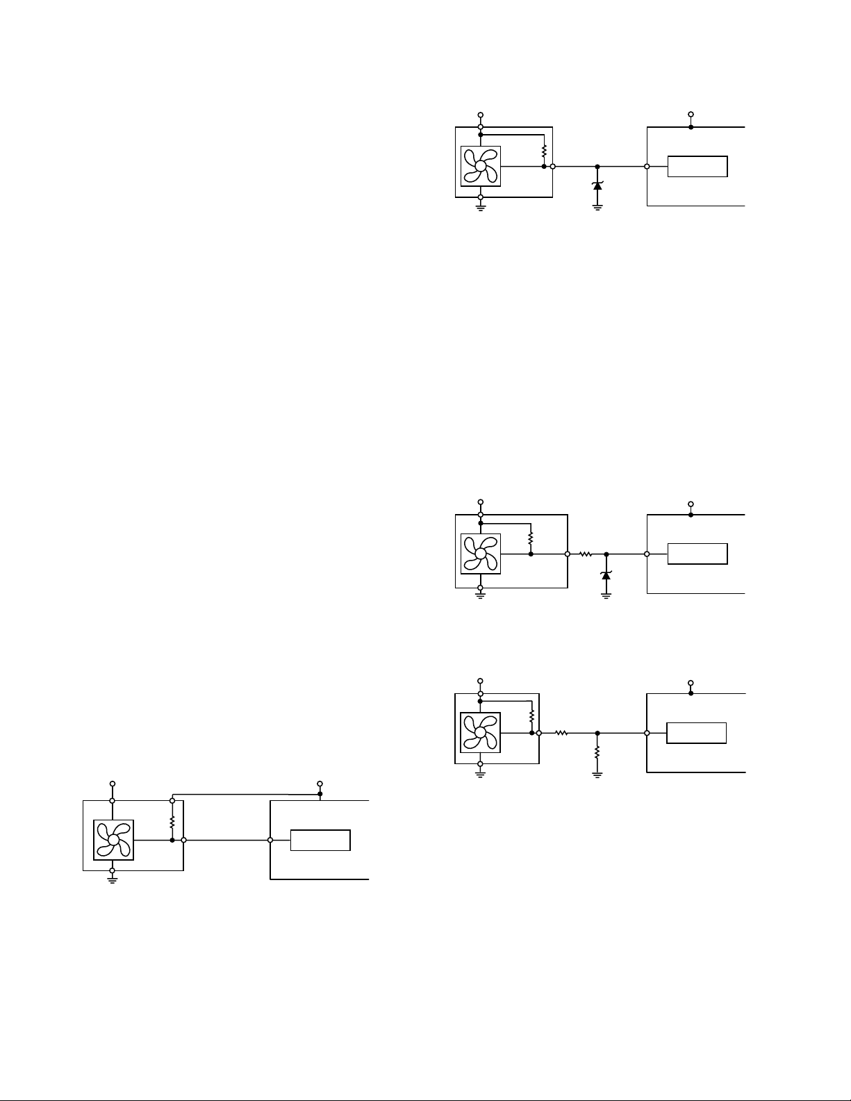
TACH SIGNAL CONDITIONING
Signal conditioning in the ADM1029 accommodates the slow
rise and fall times typical of fan tachometer outputs. The maximum input signal range is 0 V to 5 V, even if V
is less than
CC
5 V. In the event that these inputs are supplied from fan outputs
that exceed 0 V to 5 V, either resistive attenuation of the fan
signal or diode clamping must be included to keep inputs within
an acceptable range.
Figures 9a to 9d show circuits for most common fan tach outputs.
If the fan tach output has a resistive pull-up to V
, it can be
CC
connected directly to the fan input, as shown in Figure 9a.
12V
PULL-UP
4.7k
TYP
⍀
TACH
OUTPUT
TACH1
OR TACH2
Figure 9a. Fan with Tach Pull-Up to +V
V
CC
FAN SPEED
COUNTER
CC
If the fan output has a resistive pull-up to 12 V (or other voltage
greater than 6.5 V), the fan output can be clamped with a Zener
diode, as shown in Figure 9b. The Zener voltage should be
chosen so that it is greater than V
but less than 6.5 V, allowing
IH
for the voltage tolerance of the Zener. A value of between 3 V
and 5 V is suitable.
12V
PULL-UP
4.7k⍀
*CHOOSE ZD1 VOLTAGE APPROX. 0.8 ⴛ V
TYP
TACH
OUTPUT
OR TACH2
TACH1
ZD1*
ZENER
V
CC
FAN SPEED
COUNTER
CC
Figure 9b. Fan with Tach. Pull-Up to Voltage >6.5 V (e.g.,
12 V) Clamped with Zener Diode
If the fan has a strong pull-up (less than 1 kΩ) to 12 V, or a
totem-pole output, a series resistor can be added to limit the
Zener current, as shown in Figure 9c. Alternatively, a resistive
attenuator may be used, as shown in Figure 9d.
R1 and R2 should be chosen such that:
2 V < V
PULLUP
× R2/(R
+ R1 + R2) < 5 V
PULLUP
The fan inputs have an input resistance of nominally 160 kΩ to
ground, so this should be taken into account when calculating
resistor values.
With a pull-up voltage of 12 V and pull-up resistor less than
1 kΩ, suitable values for R1 and R2 would be 100 kΩ and 47 kΩ.
This will give a high input voltage of 3.83 V.
12V
TACH
O/P
PULL-UP
TYP <1k⍀
OR TOTEM-POLE
*CHOOSE ZD1 VOLTAGE APPROX. 0.8 ⴛ V
R1
10k⍀
TACH1
OR TACH2
ZD1
ZENER*
V
CC
FAN SPEED
COUNTER
CC
Figure 9c. Fan with Strong Tach. Pull-Up to >VCC or
Totem-Pole Output, Clamped with Zener and Resistor
12V
<1k⍀
R1*
TACH
OUTPUT
OR TACH2
R2*
*SEE TEXT
TACH1
V
CC
FAN SPEED
COUNTER
Figure 9d. Fan with Strong Tach. Pull-Up to >VCC or
Totem-Pole Output, Attenuated with R1/R2
FAN SPEED CONTROL
Fan speed is controlled using pulsewidth modulation (PWM).
The PWM outputs (Pins 1 and 24) give a pulse output with a
programmable frequency (default 250 Hz) and a duty-cycle
defined by the contents of the relevant fan speed register, or by
the automatic fan speed control when this mode is enabled. The
speed at which a fan runs is determined by fault conditions and
the settings of various control and mask registers.
A fan can only be driven if it is defined as being supported by
the controller in register 02h. The ADM1029 supports up to
two fans, so Bits 0 and 1 of this register are permanently set.
This register is read-only.
–14–
REV. A

ADM1029
A fan will only be driven if it is defined as being supported by
the system in register 03h. If Bit 0 of this register is set, it indicates that Fan 1 is installed. This is the power-on default. If
Bit 1 is set, it indicates that Fan 2 is installed. This bit is set by
the state of Pin 18 at power-up. This register is read/write and
the default/power-on setting can be overwritten. If a fan is not
supported in register 03h it will not be driven, even if it is physically installed.
The PWM outputs are open-drain outputs. They require pull-up
resistors and must be amplified and buffered to drive the fans.
Minimum Speed
The normal operating fan speed is set by the four LSBs of the
Fan 1 and Fan 2 Minimum/Alarm Speed Registers (addresses
60h, 61h). These bits also set the minimum speed at which a fan
will run in automatic control mode. These bits should be set to
05h. This corresponds to 33% PWM duty-cycle, which is the
lowest speed at which most fans will run reliably.
Fan(s) will run at minimum speed if there is no fault condition,
automatic fan speed is disabled, and there are no other overriding conditions.
Alarm Speed
Alarm speed is set by the four MSBs of the Fan 1 and Fan 2
Minimum/Alarm Speed Registers (addresses 60h, 61h). Fan(s)
will run at alarm speed if any of the following conditions occurs,
assuming the condition has not been masked out using the Fan
Event Mask Registers:
•
Setting Bit 0 of register 07h forces Fan 1 to run at alarm speed
(Set Fan x Alarm Speed Register).
•
Setting Bit 1 of register 07h forces Fan 2 to run at alarm speed
(Set Fan x Alarm Speed Register).
If monitoring is disabled by clearing Bit 4 of the Configuration Register, all fans controlled by the ADM1029
will run at alarm speed.
•
When a GPIO pin is configured as an input by setting Bit 0 of
the corresponding GPIO Behavior Register, and Bit 4 of the
GPIO Behavior Register is also set, all fans controlled by the
ADM1029 will go to alarm speed when the logic input is
asserted (high or low, depending on the polarity bit, Bit 1 of
the corresponding GPIO Behavior Register).
•
If Bit 7 of a Fan Fault Action Register is set (18h—Fan 1, 19h
—Fan 2) the corresponding fan will go to alarm speed when
CFAULT is pulled low by an external source.
•
If a tach measurement exceeds the set limit, all fans controlled
by the ADM1029 will run at alarm speed.
•
If a fan fault input pin is asserted (low), all fans controlled by
the ADM1029 will run at alarm speed.
•
If Bit 1 of a Temp. Fault Action Register is set (40h—Local
Sensor, 41h—Remote 1, 42h—Remote 2), all fans controlled
by the ADM1029 will go to alarm speed if the corresponding
temperature high limit is exceeded.
•
If Bit 5 of a Temp. Fault Action Register is set, all fans controlled by the ADM1029 will go to alarm speed if a temperature
input crosses the corresponding temperature low limit, the
direction depending on the setting of Bit 3 of the Temp. Control register. (0 = alarm when input goes below low limit, 1 =
alarm when input goes above low limit).
•
If Bit 1 of an AIN Behavior Register is set (50h—AIN0,
51h—AIN1), all fans controlled by the ADM1029 will go to
alarm speed if the corresponding AIN high limit is exceeded.
•
If Bit 5 of an AIN Behavior Register is set, all fans controlled
by the ADM1029 will go to alarm speed if an analog input
crosses the corresponding AIN low limit, the direction depending on the setting of Bit 3 of the AIN control register. (0 =
alarm when input goes below low limit, 1 = alarm when input
goes above low limit).
•
If a thermal override occurs while the ADM1029 is in sleep
mode, all fans controlled by the ADM1029 will run at
alarm speed.
Hot-Plug Speed
Hot-plug speed is set by the four LSBs of the Fan 1 and Fan 2
Configuration Registers (addresses 68h and 69h). The PWM
frequency is set by Bits 4 and 5 of these registers, while Bits 6
and 7 set the number of pulses per revolution for fan speed
measurement.
Fan(s) will run at hot-plug speed if any of the following conditions occur, assuming the condition has not been masked using
the Fan Event Mask Registers:
•
If a fan is unplugged, the other fan (if any) controlled by the
ADM1029 will run at hot-plug speed.
•
Setting Bit 0 of register 08h forces Fan 1 to run at hot-plug
speed (Set Fan x Hot-Plug Speed).
•
Setting Bit 1 of register 08h forces Fan 2 to run at hot-plug
speed (Set Fan x Hot-Plug Speed).
•
When a GPIO pin is configured as an input by setting Bit 0 of
the corresponding GPIO Behavior Register, and Bit 5 of the
GPIO Behavior Register is also set, all fans controlled by the
ADM1029 will go to hot-plug speed when the logic input is
asserted (high or low, depending on the polarity bit, Bit 1 of
the corresponding GPIO Behavior Register).
•
If Bit 6 of a Fan Fault Action Register is set (18h for Fan 1,
19h for Fan 2) the corresponding fan will go to hot-plug speed
when CFAULT is pulled low by an external source.
Note: If operating conditions and register settings are such that
both alarm speed and hot-plug speed would be triggered, which
one takes priority is determined by Bit 5 of the Fan 1 and Fan 2
Status Registers (addresses 10h and 11h). If this bit is set, hot-plug
speed takes priority. If it is cleared, alarm speed takes priority.
Full Speed
Fans will run at full speed if the corresponding bits in the Set
Fan x Full Speed Register (address 09h) are set: Bit 0 for Fan 1
and Bit 1 for Fan 2.
Fan Mask Registers
The effect of various conditions on fan speed can be enabled or
disabled by mask registers. In all these registers, setting Bit 0 of
the register enables Fan 1 to go to alarm speed or hot-plug speed if
the corresponding event occurs, while setting Bit 1 enables Fan
2. Clearing these bits masks the effect of the corresponding
event on fan speed.
Registers 20h and 21h are Fan Event Mask Registers. Bits 0 and
1 of register 20h enable (bit set) or mask (bit clear) the effect of
a Fan 1 fault (underspeed or fault input) on Fan 1 and Fan 2
speed. Similarly, Bits 0 and 1 of register 21h enable (bit set)
REV. A
–15–

ADM1029
or mask (bit clear) the effect of a Fan 2 Fault on Fan 1 and
Fan 2 speed.
Registers 38h to 3Eh are GPIO X Event Mask Registers. Bits 0
and 1 of these registers enable or mask the effect of a GPIO
assertion on Fan 1 and Fan 2 speed.
Note: Registers 48h to 4Ah are Temp. Cooling Action Registers. Bits 0 and 1 of these registers enable or mask the effect of
Local, Remote 1, and Remote 2 temperature faults on Fan 1
and Fan 2 speed. These registers also determine which temperature channel controls each fan in automatic fan speed control
mode, as described later.
Registers 58h and 59h are AIN Event Mask Registers. Bits 0
and 1 of these registers enable or mask the effect of an AIN outof-limit event on Fan 1 and Fan 2 speed.
MODES OF OPERATION
The ADM1029 has three different modes of operation. These
modes determine the behavior of the system.
1. PWM Duty Cycle Select Mode (directly sets fan speed under
software control).
2. Thermal Trip Mode
3. Automatic Fan Speed Control Mode
PWM DUTY CYCLE SELECT MODE
The ADM1029 may be operated under software control by
clearing bits <1:0> of the three Temp Cooling Action Registers
(Reg 0x48, 0x49, 0x4A). Once under Software Control, each
fan speed may be controlled by programming values of PWM
Duty Cycle in to the device. Values of PWM Duty Cycle between
0% to 100% may be written to the four LSBs of the Fan 1 and
Fan 2 Minimum/Alarm Speed Registers (addresses 60h, 61h).
to control the speed of each fan. Table V shows the relationship
between hex values written to the Minimum/Alarm Speed Registers and PWM duty cycle obtained.
Table V. PWM Duty Cycle Select Mode
Hex Value PWM Duty Cycle
00 0%
01 7%
02 14%
03 20%
04 27%
05 33% Recommended
06 40%
07 47%
08 53%
09 60%
0A 67%
0B 73%
0C 80%
0D 87%
0E 93%
0F 100% (Default)
It is recommended that the minimum PWM duty cycle be set to
33% (0x05). This has been determined to be the lowest PWM
*Bits <3:0> set the Minimum PWM duty cycle, bits <7:4> set the Alarm Speed
PWM duty cycle for each fan.
duty cycle that most fans will run reliably at. Note that the PWM
duty cycle values programmed in to these registers also define
the PWM duty cycle that the fans will turn on at, in Automatic
Fan Speed Control Mode. It is recommended that after powerup, the PWM duty cycle is set to 33% before enabling Automatic
Fan Speed Control.
THERMAL TRIP MODE
The ADM1029 can thermally trip the fan(s) for simple on/off
fan control, or 2-speed fan control. For example, a fan can be
programmed to run at 33% duty cycle. If the temperature exceeds
the high temperature limit set for that temperature channel, the
fan can automatically trip and run at Alarm Speed. The fan will
continue to run at Alarm Speed even if the temperature error
condition subsides, until the Latch Temp Fault bit (Bit 7 of the
Temp x Fault Action Reg) is cleared in software by writing a 0
to it. To configure Fan 1 normally, run at 33% but to thermally
trip to Alarm Speed for a Remote 2 measured temperature of
70°C, set up the following registers:
1. Configure the normal PWM duty cycle for Fan 1 to 33%.
Fan 1 Minimum/Alarm Speed Reg (0x60) = 0xF5
2. Set the Remote 2 High Temperature Limit = 70°C.
Remote 2 Temp High Limit Reg (0x92) = 0x46
3. Configure Alarm Speed on Overtemperature function for
Remote 2 Temperature channel.
Set Bit 1 of Temp 2 Fault Action Reg (0x42)
4. Enable Fan 1 to be controlled by Remote 2 Temperature.
Set Bit 0 of Temp 2 Cooling Action Reg (0x4A)
Once the fan thermally trips to Alarm Speed, it will continue to
run at Alarm Speed until the temperature drops below the High
Temperature Limit and the Latch Temp Fault bit (Bit 7 of the
Temp 2 Fault Action Reg) is cleared to 0.
EVENT LATCH BITS
Certain events that occur will cause latch bits to be set in various registers on the ADM1029. Once a latch bit is set, it will
need to be cleared by software for the system to return to normal operation. To detect if a latch bit has been set, the INT pin
can be used to signal a latch event to the system supervisor.
Alternatively, the Status Registers can be polled periodically,
and any latch bits that are set can be cleared. The events that
cause latch bits to be set are:
1. Thermal Events. If the fan is run at Alarm Speed on Overtemperature or Undertemperature, this will set the Latch
Temp Fault bit (Bit 7 of the Temp x Fault Action Registers
0x40–0x42).
2. Missing Fan. If a fan is missing, i.e., has been unplugged, the
Missing Latch bit (Bit 1 of Fan x Status Registers) is set.
3. Hotplugged Fan. If a new fan is inserted into the system, Bit
7 (Hotplug Latch bit) of the Fan x Status Register is set.
4. FAULT Asserted. If the fan becomes stuck and its FAULT
output asserts low, Bit 2 (Fault Latch bit) of the Fan x
Status register is set.
5. TACH Failure. If the fan runs underspeed or becomes stuck,
then Bit 6 (Tach Fault Latch Bit) of the Fan x Status Register is set.
–16–
REV. A

AUTOMATIC FAN SPEED CONTROL
PWM DUTY CYCLE – %
100
53
66
73
87
33
40
47
60
80
93
TEMPERATURE – ⴗC
T
MIN
T
MAX
= T
MIN
+ T
RANGE
0
5
10
20
40
80
60
T
RANGE
= 80ⴗC
T
RANGE
= 40ⴗC
T
RANGE
= 20ⴗC
T
RANGE
= 10ⴗC
T
RANGE
= 5ⴗC
PWM DUTY CYCLE – %
TEMPERATURE – ⴗC
T
MIN
T
MAX
= T
MIN
+ T
RANGE
0
20
40
80
60
T
RANGE
= 40ⴗC
T
RANGE
= 40ⴗC
T
RANGE
= 40ⴗC
100
53
66
87
40
73
33
47
60
80
93
The ADM1029 has a local temperature channel and two remote
temperature channels, which may be connected to an on-chip
diode-connected transistor on a CPU or a general-purpose
discrete transistor. These three temperature channels may be
used as the basis for an automatic fan speed control loop to
drive fans using Pulsewidth Modulation (PWM).
HOW DOES THE CONTROL LOOP WORK?
The Automatic Fan Speed Control Loop is shown in Figure 10.
ADM1029
In order for the fan speed control loop to work, certain loop
parameters need to be programmed in to the device:
1. T
2. T
3. T
4. Programmable hysteresis is included in the control loop to
REV. A
MAX
FAN SPEED
MIN
SPIN UP FOR 2 SECONDS
T
MIN
TEMPERATURE
T
MAX
= T
MIN
+ T
RANGE
Figure 10. Automatic Fan Speed Control
. This is the temperature at which a fan should switch
MIN
on and run at minimum speed. The fan will only turn on
once the temperature being measured rises above the T
MIN
value programmed. The fan will spin up for a predetermined time (default = 2 secs). See Fan Spin-Up section
for more details.
. This will be the temperature range over which the
RANGE
ADM1029 will automatically adjust fan speed. As the temperature increases beyond T
increased accordingly. The T
, the PWM duty cycle will be
MIN
parameter actually defines
RANGE
the fan speed versus temperature slope of the control loop.
. This is defined as the temperature at which a fan
MAX
will be at its maximum speed. At this temperature, the PWM
duty cycle driving the fan will be 100%. T
T
MIN
and T
+ T
RANGE
. Since this parameter is the sum of the T
RANGE
parameters, it does not need to be programmed
is given by
MAX
MIN
into a register on-chip.
prevent the fans continuously switching on and off if the
temperature is close to T
until such time as the temperature drops below T
The four MSBs of the T
0x88, 0x89, 0x8A) contain a temperature hysteresis value
that can be programmed from 0001 to 1111. This allows a
temperature hysteresis range from 1°C to 15°C for each
temperature measurement channel.
. The fans will continue to run
MIN
RANGE/THYST
registers (Registers
MIN–THYST
.
–17–
Figure 11. PWM Duty Cycle vs. Temperature Slopes
(T
)
RANGE
Figure 11 shows the different control slopes determined by the
value chosen, and programmed in to the ADM1029.
T
RANGE
T
was set to 0°C to start all slopes from the same point. It
MIN
can be seen how changing the T
value affects the PWM
RANGE
Duty Cycle vs. Temperature Slope.
Figure 12 shows how for a given T
value affects the loop. Increasing the T
the T
since T
(temperature at which the fan runs full speed) value,
MAX
MAX
= T
MIN
+ T
. Note, however, that the PWM
RANGE
, changing the T
RANGE
value will increase
MIN
MIN
Duty Cycle versus Temperature slope remains exactly the same.
Changing the T
Figure 12. Effect of Increasing T
value merely shifts the control slope.
MIN
Value on Control Loop
MIN
FAN SPIN-UP
As previously mentioned, once the temperature being measured
exceeds the T
value programmed, the fan will turn on at
MIN
minimum speed (default = 33% duty cycle). However, the problem with fans being driven by PWM is that 33% duty cycle is
not enough to reliably start the fan spinning. The solution is to

ADM1029
spin the fan up for a predetermined time, and once the fan has
spun up, its running speed may be reduced in line with the
temperature being measured.
The ADM1029 allows fan spin-up times between 1/64 second
and 16 seconds. The Fan Spin-Up Register (Register 0x0C)
allows the spin-up time for the fans to be programmed. Bit 3
of this register, when set, disables fan spin-up for both fans.
Table VI. Fan Spin-Up Times
Spin-Up Times
Bits 2:0 (Fan Spin-Up Register)
000 16 Seconds
001 8 Seconds
010 4 Seconds
011 2 Seconds (Default)
100 1 Second
101 1/4 Second
110 1/16 Second
111 1/64 Second
Once the Automatic Fan Speed Control Loop parameters have
been chosen, the ADM1029 device may be programmed. The
ADM1029 is placed into Automatic Fan Speed Control Mode
by writing to the three Temperature Cooling Action Registers
(Registers 0x48, 0x49, 0x4A). The device powers up in Automatic Fan Speed Control Mode by default, as long as the T
MIN
/
Install pin (Pin 18) does not have the disable option selected
/Install pin tied low or high). The default setting is that
(T
MIN
both fans will run at the fastest speed calculated by all three
temperature channels. The control mode offers flexibility in that
the user can decide which temperature channel/channels control
each fan (five options).
Table VII. Automatic Mode Fan Behavior
Option Temperature Cooling Action
1Bit 0 Register 0x49 and/or Bit 1 Reg 0x4A =
Remote Temp 1 Controls Fan 1, Remote Temp 2
Controls Fan 2
2Bit 0 Register 0x48 and Bit 1 Register 0x48 = 1
Local Temp Controls Fan 1 and/or Fan 2
3Bit 0 Register 0x49 and Bit 1 Register 0x49 =
Remote Temp 1 Controls Fan 1 and/or Fan 2
4Bit 0 Register 0x4A and Bit 1 Register 0x4A =
Remote Temp 2 Controls Fan 1 and/or Fan 2
5Bits 0, 1 Reg 0x48, 0x49, 0x4A = 1 Max Speed
Calculated by Local and Remote Temperature
Channels Controls Fans 1 and/or 2
When Option 5 is chosen, this offers increased flexibility. The
Local and Remote temperature channels can have independently
programmed control loops with different control parameters.
Whichever control loop calculates the fastest fan speed based on
the temperature being measured, drives both fans.
Figure 13 shows how the fan’s PWM duty cycle is determined
by two independent control loops. This is the type of Automode
Fan Behavior seen when Bits 0 and 1 of all three Temperature
Cooling Action Registers = 11. Figure 13a shows the control
loop for the Local Temperature channel. Its T
°
been programmed to 20
C, and its T
value is 40°C.
RANGE
value has
MIN
100
93
87
80
73
66
60
53
PWM DUTY CYCLE – %PWM DUTY CYCLE – %
47
40
33
02040 60
T
MIN
LOCAL TEMPERATURE – ⴗC
RANGE
T
= 40ⴗC
T
MAX
+ T
= T
MIN
RANGE
a.
100
93
87
80
73
66
60
53
47
40
33
02040 7080
T
MIN
REMOTE TEMPERATURE – ⴗC
RANGE
T
= 80ⴗC
= T
T
MAX
+ T
MIN
RANGE
b.
Figure 13. Max Speed Calculated by Local and Remote
Temperature Control Loops Drives Fans
The local temperature’s T
will thus be 60°C. Figure 13b
MAX
shows the control loop for the Remote 1 Temperature channel. Its
value has been set to 0°C, while its T
T
MIN
fore, the Remote 1 Temperature’s T
MAX
If both temperature channels measure 40
= 80°C. There-
RANGE
value will be 80°C.
°
C, both control
loops will calculate a PWM duty cycle of 66%. Therefore, the
fans will be driven at 66% duty cycle.
If both temperature channels measure 20
°
C, the local channel
will calculate 33% PWM duty cycle, while the Remote 1
channel will calculate 50% PWM duty cycle. Thus, the fans will
be driven at 50% PWM duty cycle. Consider the local temperature
°
measuring 60
°
C. The PWM duty cycle calculated by the local temperature
70
control loop will be 100% (since the temperature = T
C, while the Remote 1 temperature is measuring
). The
MAX
PWM duty cycle calculated by the Remote 1 temperature
°
control loop at 70
C will be approximately 90%. So the fans will
run full speed (100% duty cycle). Remember that the fan speed
will be based on the fastest speed calculated, and is not necessarily
based on the highest temperature measured. Depending on the
control loop parameters programmed, a lower temperature on one
channel may actually calculate a faster speed than a higher
temperature on another channel.
–18–
REV. A

ADM1029
PROGRAMMING THE AUTOMATIC FAN SPEED CONTROL LOOP
1. Program a value for T
2. Program a value for the slope T
3. T
MAX
= T
MIN
+ T
MIN
RANGE
.
.
RANGE
.
4. Program a value for Fan Spin-up Time.
5. Program the desired Automatic Fan Speed Control Mode
Behavior, i.e., which temperature channel controls each fan.
OTHER CONTROL LOOP PARAMETERS?
Having programmed all the above loop parameters, are there
any other parameters to worry about?
T
was defined as being the temperature at which a fan
MIN
switched on and ran at minimum speed. This minimum speed
should be set to 33%. If the minimum PWM duty cycle is
programmed to 33%, the fan control loops will operate as previously described.
It should be noted, however, that changing the minimum PWM
duty cycle affects the control loop behavior.
100
93
87
80
3
73
66
60
PWM DUTY CYCLE – %
53
47
40
33
0162840 60
T
MIN
2
1
= 40ⴗC
RANGE
T
TEMPERATURE – ⴗC
Figure 14. Effect of Changing Minimum Duty Cycle on
Control Loop with Fixed T
Slope 1 of Figure 14 shows T
MIN
and T
MIN
set to 0°C and the T
RANGE
Values
RANGE
chosen is 40°C. In this case, the fan’s PWM duty cycle will vary
over the range 33% to 100%. The fan will run full speed at
40°C. If the minimum PWM duty cycle at which the fan runs at
is changed, its effect can be seen on Slopes 2 and 3. Take
T
MIN
Case 2, where the minimum PWM duty cycle is reprogrammed
from 33% (default) to 53%. The fan will actually reach full speed
at a much lower temperature, 28°C. Case 3 shows that when
the minimum PWM duty cycle was increased to 73%, the temperature at which the fan ran full speed was 16°C. So the effect
of increasing the minimum PWM duty cycle, with a fixed T
and fixed T
(T
) at a lower temperature than T
MAX
be calculated?
T
MAX
, is that the fan will actually reach full speed
RANGE
MIN
+ T
RANGE
. How can
MIN
In Automatic Fan Speed Control Mode, the registers holding
the minimum PWM duty cycle at T
, are the Minimum/
MIN
Alarm Speed Registers (addresses 60h, 61h). Table VIII shows
the relationship between the decimal values written to the Minimum/Alarm Speed Registers and PWM duty cycle obtained.
Table VIII. Programming PWM Duty Cycle
Decimal Value PWM Duty Cycle
00 0%
01 7%
02 14%
03 20%
04 27%
05 33% Recommended
06 40%
07 47%
08 53%
09 60%
10 (0x0A) 67%
11 (0x0B) 73%
12 (0x0C) 80%
13 (0x0D) 87%
14 (0x0E) 93%
15 (0x0F) 100% (Default)
*Bits <3:0> set the Minimum PWM duty cycle for Automatic Mode. Bits <7:4>
set the Alarm Speed PWM duty cycle.
The temperature at which each fan will run full speed (100%
duty cycle) is given by:
T
MAX
= T
+ (( Max DC–Min DC) × T
MIN
RANGE
/10)
where,
T
T
MAX
MIN
=Temperature at which fan runs full speed
=Temperature at which fan will turn on
Max DC =Maximum Duty Cycle (100%) = 15 decimal
Min DC = Duty Cycle at T
, programmed into Fan Speed
MIN
Config Register (default = 33% = 5 decimal)
T
RANGE
=PWM Duty Cycle versus Temperature Slope
Example 1
T
MIN
=0°C, T
RANGE
= 40°C
Min DC = 53% = 8 decimal (Table VIII)
Calculate T
T
MAX
T
MAX
T
MAX
T
MAX
MAX
=T
+ (( Max DC–Min DC) × T
MIN
RANGE
/10)
=0 + ((100% DC – 53% DC) × 40/10)
=0 + ((15 – 8)× 4) = 28
= 28ⴗC. (As seen on Slope 2 of Figure 14)
Example 2
T
MIN
=0°C, T
RANGE
= 40°C
Min DC = 73% = 11 decimal (Table VIII)
Calculate T
T
MAX
T
MAX
T
MAX
T
MAX
MAX
= T
+ ((Max DC–Min DC) × T
MIN
RANGE
/10)
= 0 + ((100% DC – 73% DC) × 40/10)
= 0 + ((15 – 11) × 4) = 16
= 16ⴗC. (As seen on Slope 3 of Figure 14)
Example 3
T
MIN
= 0°C, T
RANGE
= 40°C
Min DC = 33% = 5 decimal from Table V
Calculate T
T
MAX
T
MAX
T
MAX
T
MAX
MAX
= T
+ ((Max DC–Min DC) × T
MIN
RANGE
/10)
= 0 + ((100% DC – 33% DC) × 40/10)
= 0 + ((15 – 5) × 4) = 40
= 40ⴗC. (As seen on Slope 1 of Figure 14)
REV. A
–19–

ADM1029
PROGRAM FAN
MINIMUM DUTY CYCLE
FAN 1 (REG 0x60)
FAN 2 (REG 0x61)
CONFIGURE TEMP
COOLING ACTION
LOCAL TEMP (REG 0x48)
REMOTE 1 TEMP (REG 0x49)
REMOTE 2 TEMP (REG 0x4A)
PROGRAM FAN START
TEMPERATURE, T
LOCAL TEMP (REG 0x80)
REMOTE 1 TEMP (REG 0x81)
REMOTE 2 TEMP (REG 0x82)
PROGRAM TEMP-TO-FAN
SPEED CONTROL SLOPE,
T
LOCAL TEMP (REG 0x88)
REMOTE 1 TEMP (REG 0x89)
REMOTE 2 TEMP (REG 0x8A)
CONFIGURE CONTROL
LOOP HYSTERESIS
LOCAL TEMP (REG 0x88)
REMOTE 1 TEMP (REG 0x89)
REMOTE 2 TEMP (REG 0x8A)
MIN
RANGE
REMOTE 1
TEMPERATURE
REMOTE 2
TEMPERATURE
REMOTE 1
TEMPERATURE
TEMP COOLING ACTION (CONFIGURE REG 0x48 FOR LOCAL
TEMP, REG 0x49 FOR REMOTE 1 TEMP AND REG 0x4A FOR
REMOTE 2 TEMP)
OPTION 1
OPTION 2
OPTION 3
OPTION 4
OPTION 5
BIT 0 (REG 0x49) AND/OR BIT 1 (REG 0x4A) = 1
REMOTE 1 TEMP CONTROLS FAN 1
REMOTE 2 TEMP CONTROLS FAN 2
BIT 0 (REG 0x48) AND BIT 1 (REG 0x48) = 1
LOCAL TEMP CONTROLS FAN 1 AND/OR FAN 2
BIT 0 (REG 0x49) AND BIT 1 (REG 0x49) = 1
REMOTE 1 TEMP CONTROLS FAN 1 AND/OR FAN 2
BIT 0 (REG 0x4A) AND BIT 1 (REG 0x4A) = 1
REMOTE 2 TEMP CONTROLS FAN 1 AND/OR FAN 2
BIT 0, 1 (REG 0x48, 0x49, 0x4A) = 1
FAN 1 AND/OR FAN 2 RUNS AT FASTEST SPEED
CALCULATED BY ALL TEMPERATURE CHANNELS
FAN 1
ADM1029
OPTION 1
FAN 2
FAN 1
REMOTE 1
TEMPERATURE
ADM1029
LOCAL TEMP
OPTION 2
FAN 1
FAN 2
FAN 1
CONFIGURE FAN
SPIN-UP TIME
(REGISTER 0x0C)
CONFIGURE PWM DRIVE
FREQUENCY
FAN 1 (REG 0x68)
FAN 2 (REG 0x69)
CONFIGURE TACH
OSCILLATOR FREQUENCY
FAN 1 (REG 0x68)
FAN 2 (REG 0x69)
MEASURE
FAN SPEED
FAN 1 (REG 0x70)
FAN 2 (REG 0x71)
ADM1029
REMOTE 2
TEMPERATURE
OPTION 3
REMOTE 1
TEMPERATURE
FAN 2
ADM1029
LOCAL TEMP
REMOTE 2
TEMPERATURE
OPTION 5
Figure 15. Configuring Automatic Fan Speed Control
REMOTE 2
TEMPERATURE
ADM1029
OPTION 4
FAN 1
FAN 2
FAN 2
–20–
REV. A

ADM1029
Table IX. Resistor Ratios for Setting T
and Number of Fans Installed Using TMIN/INSTALL Pin (Pin 18)
MIN
3 MSBs Ideal Ratio R1 R2 Actual Error Fans
of ADC R2/(R1 + R2) (k⍀)(k⍀) R2/(R1 + R2) (%) T
MIN
Installed
111 N/A 0 10Disabled 2
110 0.8125 18 82 0.82 0.75 48°C2
101 0.6875 22 47 0.6812 –0.63 40°C2
100 0.5625 12 15 0.5556 –0.69 32°C2
011 0.4375 15 12 0.4444 0.69 32°C1
010 0.3125 47 22 0.3188 0.63 40°C1
001 0.1875 82 18 0.18 –0.75 48°C1
000 N/A 000Disabled 1
In this case, since the Minimum Duty Cycle is the default 33%,
the equation for T
= T
T
MAX
T
= T
MAX
= T
T
MAX
T
= T
MAX
ENABLING AUTOMATIC FAN SPEED CONTROL USING TMIN/INSTALL PIN (PIN 18)
+ ((Max DC – Min DC) × T
MIN
+ ((15 – 5) × T
MIN
+ (10 × T
MIN
+ T
MIN
reduces to:
MAX
RANGE
RANGE
RANGE
/10)
/10)
RANGE
/10)
Automatic fan control can also be enabled in hardware by Pin
18 (TMIN/INSTALL). This is an 8-level input with multiple
functions, which is sampled only at power-up.
If only one fan is installed, the voltage on Pin 18 should be kept
at less than V
/2, which clears Bit 1 of register 03h. Within this
CC
voltage range, four voltage levels define the minimum temperature
at which the fan will operate in automatic speed control mode.
If two fans are installed, the voltage on Pin 18 should be between
V
/2 and VCC, which sets Bit 1 of register 03h. Within this
CC
voltage range, four voltage levels define the minimum temperature
at which the fans will operate in automatic speed control mode.
Resistor values for setting the voltage on Pin 18 are given in
Table IX. If automatic fan speed control is not used, Pin 18 can
simply be strapped to ground (one fan) or V
(two fans),
CC
depending on how many fans are installed. Under this condition, the fans will run full speed until the device is written to by
software to change fan speed.
When automatic fan speed control is enabled at power-up by
the TMIN/INSTALL pin, Bit 4 of the Configuration register is
FAN-RELATED REGISTERS
Table X is a list of registers on the ADM1029 that are specific
to fan speed measurement and control:
Table X. Fan-Specific Registers
Address Description
0x02 Fans Supported By Controller
0x03 Fans Supported In System
0x07 Set Fan x Alarm Speed
0x08 Set Fan x Hot-Plug Speed
0x09 Set Fan x Full Speed
0x10 Fan 1 Status
0x11 Fan 2 Status
0x18 Fan 1 Fault Action
0x19 Fan 2 Fault Action
0x20 Fan 1 Event Mask
0x21 Fan 2 Event Mask
0x48 Local Temp Cooling Action
0x49 Remote 1 Cooling Action
0x4A Remote 2 Cooling Action
0x60 Fan 1 Minimum/Alarm Speed
0x61 Fan 2 Minimum/Alarm Speed
0x68 Fan 1 Configuration
0x69 Fan 2 Configuration
0x70 Fan 1 Tach Value
0x71 Fan 2 Tach Value
0x78 Fan 1 Tach High Limit
0x79 Fan 2 Tach High Limit
set to enable monitoring, and Bits 0 and 1 of all Temp. Cooling
Action Registers are set, so any temperature channel will automatically control all fans that are installed.
Note: if automatic fan speed control is enabled and an event
occurs that would cause a fan to go to alarm or hot-plug speed
(e.g., temperature fault), that event will override the automatic
fan speed control. If the event affects only one fan, the other fan
will remain under automatic control.
FAN CONFIGURATION REGISTERS
Registers 0x68 and 0x69 are the Fan 1 and Fan 2 Configuration
Registers. These allow the PWM output frequencies to be selected
for each fan. The default PWM drive frequency is 250 Hz. Bits
<7:6> adjust the fan tach oscillator frequency for fan tach measurements. Bits <3:0> allow the Hot Plug PWM duty cycle value
for each fan to be programmed.
Figures 16 and 17 show how to configure the fans to handle
thermal or fault events.
REV. A
–21–

ADM1029
SET FAN 1 = 33%
SET FAN 2 = 33%
CONFIGURE FAN
NORMAL SPEED
FAN 1 (REG 0x60)
FAN 2 (REG 0x61)
FAN FAULT ACTION (CONFIGURE REG 0x18 FOR FAN 1, REG 0x19 FOR FAN 2)
BIT 0 = 1 ASSERT CFAULT ON FAN FAULT (TACH FAILURE OR FAULT ASSERTION)
BIT 1 = 1 ASSERT INT ON FAN FAULT (TACH FAILURE OR FAULT ASSERTION)
BIT 2 = 1 ASSERT CFAULT IF FAN HOT UNPLUGGED
BIT 3 = 1 ASSERT INT IF FAN HOT UNPLUGGED
BIT 4 = 1 THERMAL OVERRIDE IF IN SLEEP MODE (FAN RUNS AT ALARM SPEED)
BIT 5 = 1 DRIVE FAULT LOW IF A FAN FAULT IS DETECTED
BIT 6 = 1 IF CFAULT PULLED LOW EXTERNALLY, RUN FAN AT HOT-PLUG SPEED
BIT 7 = 1 IF CFAULT PULLED LOW EXTERNALLY, RUN FAN AT ALARM SPEED
DEFAULTS
FAN 1 = 100%
FAN 2 = 100%
DEFAULTS
FAN 1 = 100%
FAN 2 = 100%
CONFIGURE FAN
ALARM SPEED
FAN 1 (REG 0x60)
FAN 2 (REG 0x61)
CONFIGURE FAN
HOT-PLUG SPEED
FAN 1 (REG 0x68)
FAN 2 (REG 0x69)
CONFIGURE FAN FAULT
ACTION
FAN 1 (REG 0x18)
FAN 2 (REG 0x19)
CONFIGURE FAN FAULT
MASK REGISTERS
FAN 1 (REG 0x20)
FAN 2 (REG 0x21)
7 6 5 4 3 2 1 0
FAILURE OR
FAN TACH
FAILURE OR
FAULT PIN
LOW?
HAS A FAN
FAN TACH
FAILURE OR
FAULT PIN
HAS CFAULT BEEN
PULLED LOW?
LOW?
YES
UNPLUGGED?
OVER-
TEMPERATURE
DETECTED IN
SLEEP MODE?
YES
HAS A FAN
BEEN HOT
YES
BEEN HOT
UNPLUGGED?
YES
YES
FAN RUNS AT ALARM SPEED
FAN RUNS AT HOT-PLUG SPEED
FAN TACH
FAULT PIN
LOW?
YES
CFAULT
YES
INT
CFAULT
INT
HAS CFAULT BEEN
PULLED LOW?
BIT 0 = 1 RUN FAN 1 AT ALARM SPEED
BIT 1 = 1 RUN FAN 2 AT ALARM SPEED IF
BITS 2 – 7 DON'T CARE
FAN FAULT MASK (CONFIGURE REG 0x20 FOR
FAN 1, REG 0x21 FOR FAN 2)
IF FAN FAULT IS DETECTED
FAN FAULT IS DETECTED
YES
Figure 16. Fan Configuration Flowchart
FAN TACH
FAILURE OR
FAULT PIN
LOW?
FAN TACH
FAILURE OR
FAULT PIN
LOW?
FAN RUNS AT ALARM SPEED
FAN 1 RUNS ALARM SPEED
YES
FAN 2 RUNS ALARM SPEED
YES
–22–
REV. A

CONFIGURE GPIO EVENT
MASK REGISTERS
(REG 0x38 – 0x3E)
CONFIGURE TEMP
COOLING ACTION
LOCAL TEMP (REG 0x48)
REMOTE 1 TEMP (REG 0x49)
REMOTE 2 TEMP (REG 0x4A)
CONFIGURE AIN EVENT
MASK REGISTERS
AIN1 (REG 0x58)
AIN2 (REG 0x59)
GPIO EVENT MASK (CONFIGURE REG 0x38 FOR GPIO0,
REG 0x39 FOR GPIO1.....REG 0x3E FOR GPIO6)
BIT 0 = 1 FAN 1 RUNS AT ALARM OR
BIT 1 = 1 FAN 2 RUNS AT ALARM OR
BITS 2 – 7 DON'T CARE
HOT-PLUG SPEED IF GPIO PIN
IS ASSERTED
HOT-PLUG SPEED IF GPIO PIN
IS ASSERTED
PROGRAM FAN START
TEMPERATURE, T
LOCAL TEMP (REG 0x80)
REMOTE 1 TEMP (REG 0x81)
REMOTE 2 TEMP (REG 0x82)
PROGRAM TEMP-TO-FAN
SPEED CONTROL
SLOPE, T
LOCAL TEMP (REG 0x88)
REMOTE 1 TEMP (REG 0x89)
REMOTE 2 TEMP (REG 0x8A)
MIN
RANGE
AUTOMATIC FAN
SPEED CONTROL
CONFIGURATION
(REFER TO AUTOMATIC FAN SPEED
CONTROL FLOWCHART)
IS GPIO
PIN
ASSERTED?
ADM1029
YES
FAN RUNS AT ALARM
OR HOT-PLUG SPEED
CONFIGURE FAN
SPIN-UP TIME
REGISTER 0x0C
CONFIGURE PWM DRIVE
FREQUENCY
FAN1 (REG 0x68)
FAN2 (REG 0x69)
CONFIGURE TACH
OSCILLATOR FREQUENCY
FAN1 (REG 0x68)
FAN2 (REG 0x69)
MEASURE
FAN SPEED
FAN1 (REG 0x70)
FAN2 (REG 0x71)
CONFIGURE CONTROL
LOOP HYSTERESIS
LOCAL TEMP (REG 0x88)
REMOTE 1 TEMP (REG 0x89)
REMOTE 2 TEMP (REG 0x8A)
AIN EVENT MASK (CONFIGURE REG 0x58 FOR
AIN 0, REG 0x59 FOR AIN 1)
BIT 0 = 1 FAN 1 RUNS AT ALARM SPEED
BIT 1 = 1 FAN 2 RUNS AT ALARM SPEED
BITS 2 – 7 DON'T CARE
IF AIN OUT-OF-LIMIT EVENT
OCCURS
IF AIN OUT-OF-LIMIT EVENT
OCCURS
Figure 17. Fan Configuration Flowchart (Continued)
IS AIN
PIN
ASSERTED?
YES
FAN RUNS AT
ALARM SPEED
REV. A
–23–

ADM1029
RESET INPUT
Pin 12 is an active-low system RESET input. Taking this pin
low will generate a system reset, which will reset all registers to
their default values.
ANALOG INPUTS
Pins 19 and 20 of the ADM1029 are dual-function pins. They
may be configured as general-purpose logic I/O pins by setting
Bits 0, 1 of the GPIO Present/AIN Register (address 05h) or
as 0 V to 2.5 V analog inputs by clearing these bits.
In the analog input mode, Pins 19 and 20 have an input range
of 0 V to 2.5 V. By suitable input scaling, the analog input may
be configured to measure other voltage ranges such as system
power supply voltages. If more than one ADM1029 is used in a
system, several such voltages may be monitored.
The measured values of AIN0 and AIN 1 are stored in the
AIN0 and AIN1 Value Registers (addresses B8h and B9h) and
are compared to high and low limits stored in the AIN0 and
AIN1 High and Low Limit Registers (addresses A8h, A9h and
B0h, B1h).
The response of the ADM1029 to an out-of-limit measurement
on AIN0 or AIN1 depends on the status of the AIN0 and AIN1
Behavior Registers (Registers 50h, 51h). The response of
CFAULT, INT, and fan speed to temperature events depends
on the setting of these registers, as detailed in the register tables
later in this data sheet. Figure 18 shows how the AIN pins can
be configured to respond to different events.
ANALOG MONITORING CYCLE
The ADM1029 performs a sequential “round-robin,” monitoring cycle on all analog inputs and temperature inputs that are
enabled. A conversion on AIN0 or AIN1 typically takes 11.6 ms,
while an external temperature conversion takes 185.6 ms.
INTERRUPT (INT) OUTPUT
The INT output is an open-drain output with selectable polarity, intended to communicate fault conditions to the host
processor. The polarity is set to active low by clearing Bit 7 of
the Configuration Register (address 01h) or to active high by
setting this bit.
INT can be asserted if any of the following conditions occur:
•
A hot-plug event.
•
Setting Bit 6 of the Configuration Register (address 01h)
forces INT to be asserted.
•
When a GPIO pin is configured as an input by setting Bit 0 of
the corresponding GPIO Behavior Register and Bit 3 of the
GPIO Behavior Register is also set, INT will be asserted when
the logic input is asserted (high or low, depending on the polarity bit, Bit 1 of the corresponding GPIO Behavior Register).
•
If Bit 2 of a Temp. Fault Action Register is set (40h—Local
Sensor, 41h—Remote 1, 42h—Remote 2), INT will be asserted
if the corresponding temperature high limit is exceeded.
•
If Bit 6 of a Temp. Fault Action Register is set, INT will be
asserted if a temperature input crosses the corresponding
temperature low limit, the direction depending on the setting
of Bit 3 of the Temp. Fault Action register. (0 = INT when
temperature goes below low limit, 1 = INT when temperature
goes above low limit).
•
If Bit 1 of a Fan Fault Action Register (18h or 19h) is set,
INT will be asserted when a tach measurement for the corresponding fan exceeds the set limit .
•
If Bit 1 of a Fan Fault Action Register (18h or 19h) is set,
INT will be asserted when the fan fault input pin for the corresponding fan is asserted (low).
•
If Bit 2 of an AIN Behavior Register is set (50h—AIN0, 51h—
AIN1), INT will be asserted if the corresponding AIN high
limit is exceeded.
•
If Bit 6 of an AIN Behavior Register is set, INT will be asserted
if the corresponding analog input crosses its AIN low limit,
the direction depending on the setting of Bit 3 of the AIN
Behavior register. (0 = INT when input goes below low limit,
1 = INT when input goes above low limit).
FAN FREE-WHEELING TEST
The Fan Free Wheeling Test is used to diagnose fans connected
to the ADM1029 to ensure that they are operating correctly.
Large fans tightly coupled in a duct can affect each other’s airflow. If one fan has failed it may not be apparent, as the other
fan moving can suck air through the faulty fan causing it to spin.
The ADM1029 will spin each fan up separately with the other
powered down and measure the fan speed of both. When it tries
to spin the failed fan with the working fan off, the fan speed
measurement will fail, and the faulty fan will be detected. The
Fan Free-Wheel Test can be invoked at any time in software by
setting Bit 3 of the Configuration Register (Reg. 0x01). The Fan
Free-Wheel Test normally takes about 10 seconds. Once the
Fan Free-Wheel test has completed, Bit 3 will automatically
clear to 0.
Automatic Fan Free-Wheel Test
Whenever a fan is hot-plugged, the Fan Free-Wheel Test is
automatically invoked. Bit 3 gets set high automatically and once
the test has completed, self-clears to 0. If 2 fans are installed in
the system, the Fan Free-Wheel Test is invoked by removing the
suspect fan and hotplugging a new one. When the suspect fan
(e.g., Fan 1) is removed, the Missing bit (Bit 0) and Missing
Latch bit (Bit 1) of the Fan 1 Status Register are set. Fan 2 will
then automatically run at HotPlug Speed. If the faulty fan is
replaced, the HotPlug Latch bit (Bit 7) is set and the Missing
bit (Bit 0) self-clears. (However, the Missing Latch bit remains
set.) Fan 2 will return to its previous value automatically and
the Fan Free-Wheel Test is invoked. Fan 1 is run at 100% while
Fan 2 is turned off. Fan 2 is then run at 100% with Fan 1 turned
off. Both fans are then spun-up for the Fan Spin-up time. Note
that the Hotplug Latch bit and Missing Latch bit remains set
(Bits 7 and 1). These need to be cleared to 0 before a subsequent Fan Free-Wheel Test can occur. Otherwise, subsequent
fan removals and insertions are ignored.
–24–
REV. A

AIN PINS ENABLE (REG 0x05)
ENABLE PINS FOR AIN
FUNCTION
(REGISTER 0x05)
CONFIGURE AIN PINS
BEHAVIOR
AIN0 (REG 0x50)
AIN1 (REG 0x51)
CONFIGURE AIN EVENT
MASK
AIN0 (REG 0x58)
AIN1 (REG 0x59)
AIN EVENT MASK
(CONFIGURE REG 0x58 FOR
AIN0, REG 0x59 FOR AIN1)
BIT 0 = 1 RUN FAN 1 AT ALARM SPEED IF AIN OUT-OF-
LIMIT EVENT IS DETECTED
BIT 0 = 0 PIN 19 CONFIGURED AS AIN0
BIT 1 = 0 PIN 20 CONFIGURED AS AIN1
BIT 2 – 7 RESERVED FOR OTHER
AIN PINS BEHAVIOR (REG 0x50 CONFIGURES AIN0, REG 0x51 CONFIGURES AIN1)
BIT 0 = 1 CFAULT ASSERTED IF AIN VALUE EXCEEDS AIN HIGH LIMIT
BIT 1 = 1 FANS RUN ALARM SPEED IF AIN VALUE EXCEEDS AIN HIGH LIMIT
BIT 2 = 1 INT ASSERTED IF AIN VALUE EXCEEDS AIN HIGH LIMIT
BIT 3 = 0 ALARM GENERATED (INT, CFAULT, OR ALARM SPEED) WHEN AIN GOES BELOW AIN LOW LIMIT
BIT 3 = 1 ALARM GENERATED (INT, CFAULT, OR ALARM SPEED) WHEN AIN GOES ABOVE AIN LOW LIMIT
BIT 4 = 1 CFAULT ASSERTED IF AIN VALUE EXCEEDS AIN LOW LIMIT. BIT 3 DECIDES WHETHER CFAULT
BIT 5 = 1 FANS RUN ALARM SPEED IF AIN VALUE CROSSES THE AIN LOW LIMIT. BIT 3 DECIDE WHETHER
BIT 6 = 1 INT ASSERTED IF AIN VALUE CROSSES THE AIN LOW LIMIT. BIT 3 DECIDES WHETHER INT IS
BIT 7 = 1 THIS BIT LATCHES AN OUT-OF-LIMIT AIN EVENT. CLEARED BY WRITING A '0'
7 6 5 4 3 2 1 0
FUNCTIONS
IS ASSERTED GOING ABOVE OR BELOW THE LOW LIMIT
ALARM SPEED IS TRIGGERED GOING ABOVE OR BELOW THE LOW LIMIT
ASSERTED GOING ABOVE OR BELOW THE LOW LIMIT
ADM1029
IS AIN
VALUE >
AIN HIGH
LIMIT?
BIT 1 = 1 RUN FAN 2 AT ALARM SPEED IF AIN OUT-OF-
BITS 2 – 7 RESERVED – READ BACK ZERO
LIMIT EVENT IS DETECTED
CONFIGURE AIN
HIGH LIMITS
AIN0 (REG 0xA8)
AIN1 (REG 0xA9)
CONFIGURE AIN
LOW LIMITS
AIN0 (REG 0xB0)
AIN1 (REG 0xB1)
MEASURE AIN
VOLTAGES
AIN0 (REG 0xB8)
AIN1 (REG 0xB9)
Figure 18. Configuring AIN0 and AIN1 Pins
HAS AIN VALUE
EXCEEDED AIN
LOW LIMIT?
YES
HAS AIN VALUE
EXCEEDED AIN
LOW LIMIT?
YES
HAS AIN VALUE
EXCEEDED AIN
LOW LIMIT?
YES
AIN ABOVE OR
BELOW LOW AIN
LIMIT?
IS AIN
VALUE >
AIN HIGH
LIMIT?
YES
IS AIN
VALUE >
AIN HIGH
LIMIT?
YES
0 = ALARM BELOW AIN LOW LIMIT
1 = ALARM ABOVE AIN LOW LIMIT
YES
FANS RUN ALARM SPEED
FANS RUN ALARM SPEED
CFAULT
INT
CFAULT
INT
REV. A
–25–

ADM1029
GENERAL PURPOSE LOGIC INPUT/OUTPUTS
The ADM1029 has six dual-function pins (see Pin Function
Descriptions section) that may be configured as general-purpose
Logic I/O pins by setting the appropriate bit(s) of the GPIO
Present/AIN Register (address 05h) or as their alternate functions by clearing these bits.
When configured as GPIO pins, each GPIO pin has a Behavior
Register associated with it (Registers 28h to 2Eh) that may be
used to configure the operation of the pin.
The GPIO pins may be configured as inputs or outputs. When
used as inputs, they may be configured to:
•
Be active high or active low.
•
Set/clear a bit in the Behavior Register when GP input is
asserted/deasserted.
•
Latch a bit in the Behavior Register when GP input is asserted
(must be cleared by software).
•
Assert CFAULT when GP input asserted.
•
Assert INT when GP input asserted.
•
Set fan(s) to alarm speed when GP input asserted.
•
Set fan(s) to hot-plug speed when GP input asserted.
When used as outputs, they may be configured to:
•
Be active high or low
•
Be asserted if a High Temperature Limit is exceeded.
•
Be asserted if a temperature measurement falls below a
low limit.
•
Be asserted if a fan fault is detected.
•
Be asserted if a fan tach limit is exceeded.
•
Be asserted if an AIN high limit is exceeded.
•
Be asserted if an analog input falls below a low limit.
Figure 19 shows how to configure the GPIO pins to handle
different out-of-limit and fault events.
CFAULT OUTPUT
The Cascade Fault output (CFAULT), is an open-drain, active
low output, intended to communicate fault conditions to other
ADM1029s in a system, without the intervention of the host processor. The other ADM1029’s may then adjust their fans’ speed
to compensate, depending on the settings of various registers.
CFAULT is asserted if any of the following conditions occurs:
•
A hot-plug event.
•
Setting Bit 5 of the Configuration Register (address 01h)
forces CFAULT to be asserted.
•
When a GPIO pin is configured as an input by setting Bit 0 of
the corresponding GPIO Behavior Register and Bit 2 of the
GPIO Behavior Register is also set, CFAULT will be asserted
when the logic input is asserted (high or low depending on the
polarity bit, Bit 1 of the corresponding GPIO Behavior Register).
•
If Bit 0 of a Temp. Fault Action Register is set (40h—Local
Sensor, 41h—Remote 1, 42h—Remote 2), CFAULT will be
asserted if the corresponding temperature high limit is exceeded.
•
If Bit 4 of a Temp. Fault Action Register is set, CFAULT will
be asserted if a temperature input crosses the corresponding
temperature low limit, the direction depending on the setting
of Bit 3 of the Temp. Fault Action Register. (0 = CFAULT
when input goes below low limit, 1 = CFAULT when input
goes above low limit).
•
If Bit 0 of a Fan Fault Action Register (18h or 19h) is set,
CFAULT will be asserted when a tach measurement for the
corresponding fan exceeds the set limit.
•
If Bit 0 of a Fan Fault Action Register (18h or 19h) is set,
CFAULT will be asserted, when the fan fault input pin for
the corresponding fan is asserted (low).
•
If Bit 0 of an AIN Behavior Register is set (50h—AIN0,
51h—AIN1), CFAULT will be asserted if the corresponding
AIN high limit is exceeded.
•
If Bit 4 of an AIN Behavior Register is set, CFAULT will be
asserted if an analog input crosses the corresponding AIN low
limit, the direction depending on the setting of Bit 3 of the
AIN Behavior Register. (0 = CFAULT when input goes
below low limit, 1 = CFAULT when input goes above low limit).
–26–
REV. A

ENABLE PINS FOR GPIO
FUNCTION
(REGISTER 0x05)
GPIO PINS ENABLE (REG 0x05)
BIT 0 = 1 PIN 19 CONFIGURED AS GPIO0
BIT 1 = 1 PIN 20 CONFIGURED AS GPIO1
BIT 2 = 1 PIN 11 CONFIGURED AS GPIO2
BIT 3 = 1 PIN 13 CONFIGURED AS GPIO3
BIT 4 = 1 PIN 14 CONFIGURED AS GPIO4
BIT 5 = 1 PIN 16 CONFIGURED AS GPIO5
BIT 6 = 1 PIN 17 CONFIGURED AS GPIO6
BIT 7 RESERVED
ADM1029
CONFIGURE GPIO PINS
BEHAVIOR
GPIO0 (REG 0x28)
|
GPIO6 (REG 0x2E)
CONFIGURE GPIO EVENT
MASK
GPIO0 (REG 0x38)
|
GPIO6 (REG 0x3E)
BIT 0 = 1 RUN FAN 1 AT ALARM OR HOT-PLUG SPEED IF GPIO PIN IS ASSERTED
BIT 1 = 1 RUN FAN 2 AT ALARM OR HOT-PLUG SPEED IF GPIO PIN IS ASSERTED
BITS 2 – 7 RESERVED – READ BACK ZERO
GPIO EVENT MASK (CONFIGURE REG 0x38 FOR GPIO0, REG 0x39 FOR
GPIO1.....REG 0x3E FOR GPIO6)
GPIO PINS BEHAVIOR (REG 0x28 CONFIGURES GPIO0, REG 0x29 CONFIGURES GPIO1, ETC.)
BIT 0 SETS THE DIRECTION FOR GPIO PIN. A '0' CONFIGURES THE PIN AS AN OUTPUT, A '1' SETS
BIT 1 SETS THE POLARITY FOR GPIO PIN. A '0' MAKES THE PIN ACTIVE LOW, A '1' MAKES THE PIN
BIT 2 = 1 IF GPIO PIN IS CONFIGURED AS AN INPUT, CFAULT IS ASSERTED WHEN GPIO IS ASSERTED.
BIT 3 = 1 IF GPIO PIN IS CONFIGURED AS AN INPUT, INT IS ASSERTED WHEN GPIO IS ASSERTED. IF GPIO
BIT 4 = 1 IF GPIO PIN IS CONFIGURED AS AN INPUT, FANS GO TO ALARM SPEED IF GPIO IS ASSERTED. IF
BIT 5 = 1 IF GPIO PIN IS CONFIGURED AS AN INPUT, FANS GO TO HOT-PLUG SPEED IF GPIO IS ASSERTED.
BIT 6 = 1 IF GPIO PIN IS AN INPUT, THIS BIT REFLECTS THE STATE OF GPIO PIN. IF GPIO PIN IS AN
BIT 7 IF GPIO PIN IS AN INPUT, THIS BIT LATCHES A GPIO ASSERTION EVENT. CLEARED BY
THE PIN UP AS AN INPUT
ACTIVE HIGH
IF GPIO PIN IS CONFIGURED AS AN OUTPUT, GPIO PIN WILL BE ASSERTED IF A HIGH
TEMPERATURE LIMIT IS EXCEEDED. THIS CAN BE USED TO SHUT DOWN THE SYSTEM IN AN
OVER-TEMPERATURE SITUATION.
PIN IS AN OUTPUT, GPIO IS ASSERTED IF A TEMPERATURE LOW LIMIT IS EXCEEDED.
GPIO PIN IS AN OUTPUT, GPIO IS ASSERTED IF A FAN TACH LIMIT IS EXCEEDED.
IF GPIO PIN IS AN OUTPUT, GPIO IS ASSERTED IF A FAN FAULT IS DETECTED (FAULT PIN).
OUTPUT, GPIO IS ASSERTED IF AN AIN HIGH LIMIT IS EXCEEDED.
WRITING A '0.' IF GPIO PIN IS AN INPUT, GPIO IS ASSERTED IF AN AIN LOW LIMIT IS EXCEEDED.
IS GPIO
PIN ASSERTED?
IS GPIO
PIN ASSERTED?
FAN 1 RUNS AT HOT-PLUG
OR ALARM SPEED
YES
FAN 2 RUNS AT HOT-PLUG
OR ALARM SPEED
YES
Figure 19. Configuring GPIO Pins
REV. A
–27–

ADM1029
Table XI. Register Map
Address Name Default Value Description
00 Status Register 00h Contains the status of various fault conditions.
01 Config Register 0000 0000 Configures the operation of the device.
02 Fan Supported By Controller 03h Contains the number of fans the device can support.
03 Fans Supported In System 0000 00?1 Contains the number of fans actually supported by the device
in the application.
04 GPIOs Supported By Controller 7Fh Contains the number of GPIO pins the device can support.
05 GPIO Present/AIN 0????111 Used to configure GPIO pins as GPIO or as their alternate
analog input function.
06 Temp Devices Installed 0000 0??1 Contains number of temperature sensors installed.
07 Set Fan x Alarm Speed 00h Writing to appropriate bit(s) makes fan(s) run at alarm speed.
08 Set Fan x Hot-Plug Speed 00h Writing to appropriate bit(s) makes fan(s) run at hot-plug speed.
09 Set Fan x Full Speed 00h Writing to appropriate bit(s) makes fan(s) run at full speed.
0B S/W RESET 00h Writing A6h to this register causes a software reset.
0C Fan Spin-Up 03h Configures fan spin-up time.
0D Manufacturer’s ID 41h This register contains the manufacturer’s ID code for the device.
0E Major/Minor Revision 00h Contains the manufacturer’s code for major and minor revi-
sions to the device in two nibbles.
0F Manufacturer’s Test Register 00h This register is used by the manufacturer for test purposes. It
should not be read from or written to in normal operation.
10 Fan 1 Status 0000 0?0? Contains status information for FAN 1.
11 Fan 2 Status 0000 0?0? Contains status information for FAN 2.
18 Fan 1 Fault Action BFh Sets operation of INT, CFAULT, etc., for FAN 1 fault.
19 Fan 2 Fault Action BFh Sets operation of INT, CFAULT, etc., for FAN 2 fault.
20 Fan 1 Event Mask FFh Enables/disables FAN 1 and/or FAN 2 alarm/hot-plug speed
in response to a fault or hot-plug event on FAN 1.
21 Fan 2 Event Mask FFh Enables/disables FAN 1 and/or FAN 2 alarm/hot-plug speed
in response to a fault or hot-plug event on FAN 2.
28 GPIO0 Behavior 00h Configures the operation of GPIO0.
29 GPIO1 Behavior 00h Configures the operation of GPIO1.
2A GPIO2 Behavior 00h Configures the operation of GPIO2.
2B GPIO3 Behavior 00h Configures the operation of GPIO3.
2C GPIO4 Behavior 00h Configures the operation of GPIO4.
2D GPIO5 Behavior 00h Configures the operation of GPIO5.
2E GPIO6 Behavior 00h Configures the operation of GPIO6.
30 Local Temperature Offset 00h Offset register for local temperature measurement. The value
in this register is added to the local temperature value to reduce
system offset effects.
31 Remote 1 Temperature Offset 00h Offset register for first remote temperature channel (D1). The
value in this register is added to the temperature value to reduce
system offset effects.
32 Remote 2 Temperature Offset 00h Offset register for second remote temperature channel (D2).
The value in this register is added to the temperature value to
reduce system offset effects.
38 GPIO0 Event Mask 00h Enables/disables FAN 1 and/or FAN 2 alarm/hot-plug speed
in response to GPIO0 being asserted.
39 GPIO1 Event Mask 00h Enables/disables FAN 1 and/or FAN 2 alarm/hot-plug speed
in response to GPIO1 being asserted.
3A GPIO2 Event Mask 00h Enables/disables FAN 1 and/or FAN 2 alarm/hot-plug speed
in response to GPIO2 being asserted.
3B GPIO3 Event Mask 00h Enables/disables FAN 1 and/or FAN 2 alarm/hot-plug speed
in response to GPIO3 being asserted.
–28–
REV. A

ADM1029
Table XI. Register Map (Continued)
Address Name Default Value Description
3C GPIO4 Event Mask 00h Enables/disables FAN 1 and/or FAN 2 alarm/hot-plug speed
in response to GPIO4 being asserted.
3D GPIO5 Event Mask 00h Enables/disables FAN 1 and/or FAN 2 alarm/hot-plug speed
in response to GPIO5 being asserted.
3E GPIO6 Event Mask 00h Enables/disables FAN 1 and/or FAN 2 alarm/hot-plug speed
in response to GPIO6 being asserted.
40 Local Temp Fault Action 08h Configures the operation of INT, CFAULT, etc. for a Local
Temp fault (internal temperature sensor).
41 Remote 1 Temp Fault Action 08h Configures the operation of INT, CFAULT, etc. for a Remote
1 Temp fault (D1 Temperature Sensor).
42 Remote 2 Temp Fault Action 08h Configures the operation of INT, CFAULT, etc. for a Remote
2 Temp fault (D2 Temperature Sensor).
48 Local Temp Cooling Action 00h Enables/disables FAN 1 and/or FAN 2 alarm/hot-plug speed
in response to a Local Temp event (internal temperature sensor).
49 Remote 1 Temp Cooling Action 00h Enables/disables FAN 1 and/or FAN 2 alarm/hot-plug speed
in response to a Remote 1 Temp event (D1 temperature sensor).
4A Remote 2 Temp Cooling Action 00h Enables/disables FAN 1 and/or FAN 2 alarm/hot-plug speed
in response to a Remote 2 Temp event (D2 temperature sensor).
50 AIN0 Behavior 00h Configures the operation of INT, CFAULT, etc. for a fault on
Analog Channel 0.
51 AIN1 Behavior 00h Configures the operation of INT, CFAULT, etc. for a fault on
Analog Channel 1.
58 AIN0 Event Mask 00h Enables/disables FAN 1 and/or FAN 2 alarm/hot-plug speed
in response to a fault on Channel 0.
59 AIN1 Event Mask 00h Enables/disables FAN 1 and/or FAN 2 alarm/hot-plug speed
in response to a fault on Channel 1.
60 Fan 1 Minimum/Alarm Speed FFh Contains the Minimum/Alarm speeds for Fan 1.
61 Fan 2 Minimum/Alarm Speed FFh Contains the Minimum/Alarm speeds for Fan 2.
68 Fan 1 Configuration 2Fh Configures hot-plug speed, PWM and tach frequency.
69 Fan 2 Configuration 2Fh Configures hot-plug speed, PWM and tach frequency.
70 Fan 1 Tach Value 00h Contains the measured value from the FAN 1 tachometer output.
71 Fan 2 Tach Value 00h Contains the measured value from the FAN 2 tachometer output.
78 Fan 1 Tach High Limit FFh Contains the high limit for FAN 1 tachometer measurement.
79 Fan 2 Tach High Limit FFh Contains the high limit for FAN 2 tachometer measurement.
80 Local Temp T
MIN
81 Remote 1 Temp T
82 Remote 2 Temp T
88 Local Temp T
RANGE/THYST
89 Remote 1 Temp T
MIN
MIN
RANGE/THYST
??h Defines the starting temperature for the fan when controlled
by the local temperature channel, under Automatic Fan
Speed Control.
??h Defines the starting temperature for the fan when controlled
by the Remote 1 temperature channel, under Automatic Fan
Speed Control. (D1 Temp Sensor).
??h Defines the starting temperature for the fan when controlled
by the Remote 2 temperature channel, under Automatic Fan
Speed Control. (D2 Temp Sensor).
51h This register programs the control range for the local tempera-
ture control loop. It also defines the amount of temperature
hysteresis applied to the loop.
51h This register programs the control range for the Remote 1
temperature control loop. It also defines the amount of tem-
perature hysteresis applied to the loop.
REV. A
–29–

ADM1029
Table XI. Register Map (Continued)
Address Name Default Value Description
8A Remote 2 Temp T
90 Local Temp High Limit 50h (80°C) High limit for Local measurement (internal sensor).
91 Remote 1 Temp High Limit 64h (100°C) High limit for Remote 1 measurement (D1 Sensor).
92 Remote 2 Temp High Limit 64h (100°C) High limit for Remote 2 measurement (D2 Sensor).
98 Local Temp Low Limit 3Ch (60°C) Low limit for Local Temp measurement (internal sensor).
99 Remote 1 Temp Low Limit 46h (70°C) Low limit for Remote 1 measurement (D1 Sensor).
9A Remote 2 Temp Low Limit 46h (70°C) Low limit for Remote 2 measurement (D2 Sensor).
A0 Local Temp Value 00h Measured value from local temp sensor.
A1 Remote 1 Temp Value 00h Measured value from D1 Remote Sensor.
A2 Remote 2 Temp Value 00h Measured value from D2 Remote Sensor.
A8 AIN0 High Limit FFh High limit for measurement on analog Channel 0.
A9 AIN1 High Limit FFh High limit for measurement on analog Channel 1.
B0 AIN0 Low Limit 00h Low limit for measurement on analog Channel 0.
B1 AIN1 Low Limit 00h Low limit for measurement on analog Channel 1.
B8 AIN0 Measured Value 00h Measured value of analog Channel 0.
B9 AIN1 Measured Value 00h Measured value of analog Channel 1.
NOTE
Question marks on this and following pages indicate bit settings that depend on the state of certain pins on power-up.
RANGE/THYST
51h This register programs the control range for the Remote 2
temperature control loop. It also defines the amount of temperature hysteresis applied to the loop.
–30–
REV. A

ADM1029
CONFIGURATION REGISTERS
Register 01h — Config Register (Power-On Default 000? 000?)
Bit Name R/W Description
0 Install = ? R/W This bit reflects Bit 1 of Register 0x03 (Fans Supported In System).
1Global INT mask = 0 R/W Setting this bit to 1 will disable the INT output for all interrupt sources.
2 ARA Disable = 0 R/W Setting this bit to 1 will disable the SMBus Alert Response Address feature.
3Perform Free-Wheel R/W Setting this bit to 1 will initiate the Fan Free-Wheeling Test. While this test
Test = 0 is being performed normal monitoring of fan speeds, temperature and volt-
ages will be temporarily halted. This bit will automatically reset to 0 once the
test is complete which will take about 10 seconds.
4 Start Monitoring = 0 R/W Set to 1 to start round robin monitoring cycle of voltage temperature and fan
speeds, fault detection, etc. While this bit is 0, all fans will run at Alarm
Speed. This bit is set at power-up; otherwise, if automatic fan speed control
is enabled by Pin 18.
5Force CFAULT = 0 R/W Setting this bit to 1 forces CFAULT to be asserted (Low).
6Force INT = 0 R/W Setting this bit to 1 forces INT to be asserted (Polarity depends on Bit 7).
7 INT Polarity = 0 R/W Polarity of INT when asserted. 1 means High and 0 means Low.
NOTE
Question marks on this and following pages indicate bit settings that depend on the state of certain pins on power-up.
Register 05h – GPIO Present / AIN (Power-On Default 0????111)
Bit Name R/W Description
0 GPIO 0 = 1 R/W Indicates that GPIO0 is being used. Set to 1 on power-up, but can be over-
written by software. Setting this bit to 0 means AIN0 is being used.
1 GPIO 1 = 1 R/W Indicates that GPIO1 is being used. Set to 1 on power-up, but can be over-
written by software. Setting this bit to 0 means AIN1 is being used.
2 GPIO 2 = 1 R/W Indicates that GPIO2 is being used. Set to 1 on power-up, but can be over-
written by software.
3 GPIO 3 = ? R/W Indicates that GPIO3 is being used. Setting this bit to 0 means TDM1 is
being used. The ADM1029 can detect on power-up if TDM1 is connected.
If so, this bit is set to 0, otherwise it is set to 1. The default setting can be
overwritten by software.
4 GPIO 4 = ? R/W Indicates that GPIO4 is being used. Setting this bit to 0 means TDM1 is
being used. The ADM1029 can detect on power-up if TDM1 is connected.
If so, this bit is set to 0, otherwise it is set to 1. The default setting can be
overwritten by software.
5 GPIO 5 = ? R/W Indicates that GPIO5 is being used. Setting this bit to 0 means TDM2 is
being used. The ADM1029 can detect on power-up if TDM2 is connected.
If so, this bit is set to 0, otherwise it is set to 1. The default setting can be
overwritten by software.
6 GPIO 6 = ? R/W Indicates that GPIO6 is being used. Setting this bit to 0 means TDM2 is
being used. The ADM1029 can detect on power-up if TDM2 is connected.
If so, this bit is set to 0, otherwise it is set to 1. The default setting can be
overwritten by software.
7Reserved R Unused. Will read back 0.
NOTE
Question marks on this and following pages indicate bit settings that depend on the state of certain pins on power-up.
REV. A
–31–

ADM1029
Register 07h – Set Fan x* Alarm Speed (Power-On Default 00h)
Bit Name R/W Description
0Fan 1 Alarm Speed = 0 R/W When set to 1, Fan 1 will run at Alarm Speed.
1Fan 2 Alarm Speed = 0 R/W When set to 1, Fan 2 will run at Alarm Speed.
2Reserved R Unused. Will read back 0.
3Reserved R Unused. Will read back 0.
4Reserved R Unused. Will read back 0.
5Reserved R Unused. Will read back 0.
6Reserved R Unused. Will read back 0.
7Reserved R Unused. Will read back 0.
NOTES
*“x” denotes the fan number.
Question marks on this and following pages indicate bit settings that depend on the state of certain pins on power-up.
Register 08h – Set Fan x* Hot-Plug Speed (Power-On Default 00h)
Bit Name R/W Description
0 Fan 1 Hot-Plug Speed = 0 R/W When set to 1, Fan 1 will run at Hot-Plug Speed.
1 Fan 2 Hot-Plug Speed = 0 R/W When set to 1, Fan 2 will run at Hot-Plug Speed.
20 RUnused. Will read back 0.
30 RUnused. Will read back 0.
40 RUnused. Will read back 0.
50 RUnused. Will read back 0.
60 RUnused. Will read back 0.
70 RUnused. Will read back 0.
NOTES
*“x” denotes the fan number.
Question marks on this and following pages indicate bit settings that depend on the state of certain pins on power-up.
Register 09h – Set Fan x* Full Speed (Power-On Default 00h)
Bit Name R/W Description
0Fan 1 Full Speed = 0 R/W When set to 1 Fan 1 will run at Full Speed.
1Fan 2 Full Speed = 0 R/W When set to 1 Fan 2 will run at Full Speed.
2Reserved R Unused. Will read back 0.
3Reserved R Unused. Will read back 0.
4Reserved R Unused. Will read back 0.
5Reserved R Unused. Will read back 0.
6Reserved R Unused. Will read back 0.
7Reserved R Unused. Will read back 0.
NOTES
*“x” denotes the fan number.
Question marks on this and following pages indicate bit settings that depend on the state of certain pins on power-up.
–32–
REV. A

ADM1029
STATUS REGISTERS
Register 00h – Status Register (Power-On Default 00h)
Bit Name R/W Description
0 INT RThis bit is set to 1 when the device is asserting INT low. This bit is the logical
OR of several bits in other registers and is cleared when these bits are cleared.
1 CFAULT_in R This bit is set to 1 when the device is receiving CFAULT low from another device.
2 CFAULT_out R This bit is set to 1 when the device is asserting CFAULT low. This bit is
the logical OR of several bits in other registers and is cleared when these
bits are cleared.
3 In Alarm_speed R This bit is set to 1 when either fan is running at Alarm Speed. This bit is the
logical OR of several bits in other registers and is cleared when these bits are
cleared.
4 In Hot-Plug Speed R This bit is set to 1 when either fan is running at Hot-Plug Speed. This bit is
the logical OR of several bits in other registers and is cleared when these bits
are cleared.
5 GPIO/AIN Event R This bit is a logical OR of Bits 1, 3, 6, and 7 in the GPIO Behavior Registers
at 28h to 2Eh while they are configured as inputs, and Bit 7 in the AIN
Behavior Registers at 50h and 51h. It will be set when any of these bits are set
and cleared when all of these bits are cleared.
6Hot Plug/Fan Fault R This bit is a logical OR of Bits 1, 3, 6, and 7 in the Fan Status Registers at
10h and 11h. It will be set when any of these bits are set and cleared when all
of these bits are cleared.
7Thermal Event R This bit is a logical OR of Bit 7 in the Temp Fault Action Registers at 40h,
41h, and 42h. It will be set when any of these bits are set and cleared when all
of these bits are cleared.
Register 02h – Fan Supported By Controller (Power-On Default 03h)
Bit Name R/W Description
0Fan 1 = 1 R This bit set to 1 means the ADM1029 can support Fan 1.
1Fan 2 = 1 R This bit set to 1 means the ADM1029 can support Fan 2.
2Reserved R Unused. Will read back 0.
3Reserved R Unused. Will read back 0.
4Reserved R Unused. Will read back 0.
5Reserved R Unused. Will read back 0.
6Reserved R Unused. Will read back 0.
7Reserved R Unused. Will read back 0.
Register 03h – Fans Supported In System (Power-On Default 0000 00?1)
Bit Name R/W Description
0Fan 1 = 1 R/W Indicates that Fan 1 is being used. Set to 1 on Power-up, but can be over-
written by software.
1Fan 2 = ? R/W Indicates that Fan 2 is being used. Set by Pin 18 (TMIN/INSTALL) on
Power-up, but can be overwritten by software.
2Reserved R Unused. Will read back 0.
3Reserved R Unused. Will read back 0.
4Reserved R Unused. Will read back 0.
5Reserved R Unused. Will read back 0.
6Reserved R Unused. Will read back 0.
7Reserved R Unused. Will read back 0.
NOTE
Question marks on this and following pages indicate bit settings that depend on the state of certain pins on power-up.
REV. A
–33–

ADM1029
Register 04h – GPIOs Supported By Controller (Power-On Default 7Fh)
Bit Name R/W Description
0 GPIO 0 = 1 (Pin 19) R This bit set to 1 means the ADM1029 can support GPIO0, available on
Pin 19.
1 GPIO 1 = 1 (Pin 20) R This bit set to 1 means the ADM1029 can support GPIO1, available on
Pin 20.
2 GPIO 2 = 1 (Pin 11) R This bit set to 1 means the ADM1029 can support GPIO2, available on
Pin 11.
3 GPIO 3 = 1 (Pin 13) R This bit set to 1 means the ADM1029 can support GPIO3, available on
Pin 13.
4 GPIO 4 = 1 (Pin 14) R This bit set to 1 means the ADM1029 can support GPIO4, available on
Pin 14.
5 GPIO 5 = 1 (Pin 16) R This bit set to 1 means the ADM1029 can support GPIO5, available on
Pin 16.
6 GPIO 6 = 1 (Pin 17) R This bit set to 1 means the ADM1029 can support GPIO6, available on
Pin 17.
7Reserved R Unused. Will read back 0.
Register 06h – Temp Devices Installed (Power-On Default 0000 0??1)
Bit Name R/W Description
0Local Temp = 1 R This bit is permanently set to 1 since the local temperature sensor is
always available.
1Remote 1 Temp = ? R This bit is set to 1 if the Remote 1 temperature sensor (TDM1) is installed.
(Automatically detected on power-up.)
2Remote 2 Temp = ? R This bit is set to 1 if the Remote 2 temperature sensor (TDM2) is installed.
(Automatically detected on power-up.)
3Reserved R Unused. Will read back 0.
4Reserved R Unused. Will read back 0.
5Reserved R Unused. Will read back 0.
6Reserved R Unused. Will read back 0.
7Reserved R Unused. Will read back 0.
NOTE
Question marks on this and following pages indicate bit settings that depend on the state of certain pins on power-up.
–34–
REV. A

ADM1029
Register 10h, 11h – Fan x* Status (Power-On Default 0000 0?0?)
Bit Name R/W Description
0Missing = x R Reflects the state of Pins 4/21. Low means Fan x* is installed, High
means it is missing. This bit will automatically return Low if a missing
fan is replaced.
1Missing _L = 0 R/W This bit is edge-triggered and latches a Fan x* missing event on removal
of Fan x. This bit is cleared by writing a 0 to it.
2Fault_ = x R Inverse of Pin 2/23. Low on pin means Fan x* has a fault (Pins 2/23
Low), High on pin means it is OK. This bit will automatically return
Low if Pins 2/23 goes high.
3Fault_L_ = 0 R/W This bit is edge-triggered and latches a Fan x* fault event on Pins 2/23.
This bit is cleared by writing a 0 to it. If the PRESENT pin for a fan
input is high (fan not installed) this bit will be cleared automatically.
4 Sleep = 0 R/W When this bit is set, Fan x* will be stopped and no Fan x* faults will be
monitored. If Bit 4 in Fan x* Fault Action Register is set, Fan x* will go
to Alarm Speed if an overtemperature event is detected as per settings in
the Temp Fault Action Registers.
5Hot Plug Priority R/W This bit indicates whether Fan x runs at Hot-Plug Speed (bit set to 1) or
Alarm Speed (bit set to 0) if both modes are triggered.
6 Tach_Fault_L R/W Latches a Fan x Tach Fault. This bit is cleared by writing a 0 to it. If the
PRESENT pin for a fan input is high (fan not installed), this bit will be
cleared automatically.
7 Hot_Plug_L R/W This bit is edge-triggered and latches a Fan x Hot-plug event which is the
insertion of Fan x. (Note difference to Bit 1.) This bit is cleared by writing a 0 to it. If a fan is Hot-Plug installed, it will run at Normal Speed.
NOTES
*“x” denotes the fan number. Register 10h is for Fan 1 and Register 11h is for Fan 2.
Question marks on this and following pages indicate bit settings that depend on the state of certain pins on power-up.
REV. A
–35–

ADM1029
TEMPERATURE REGISTERS
Register 06h – Temp Devices Installed (Power-On Default 0000 0??1)
Bit Name R/W Description
0Local Temp = 1 R This bit is permanently set to 1 since the local temperature sensor is always
available.
1Remote 1 Temp = ? R This bit is set to 1 if the Remote 1 temperature sensor (TDM1) is installed.
(Automatically detected on power-up.)
2Remote 2 Temp = ? R This bit is set to 1 if the Remote 2 temperature sensor (TDM2) is installed.
(Automatically detected on power-up.)
3Reserved R Unused. Will read back 0.
4Reserved R Unused. Will read back 0.
5Reserved R Unused. Will read back 0.
6Reserved R Unused. Will read back 0.
7Reserved R Unused. Will read back 0.
NOTE
Question marks on this and following pages indicate bit settings that depend on the state of certain pins on power-up.
Register 30h, 31h, 32h – Temp x* Offset Registers (Power-On Default 00h)
Bit Name R/W Description
<7:0> Offset R/W This register contains an offset value that is automatically added to the tem-
perature value to reduce the effects of systemic offset errors.
*“x” denotes the number of the temperature channel. Register 30h is for Local temperature channel, 31h is for Remote 1 Temp (D1), 32h is for Remote 2 Temp (D2).
Register 40h, 41h, 42h – Temp x* Fault Action (Power-On Default 08h)
Bit Name R/W Description
0Assert CFAULT on R/W When this bit is set, CFAULT will be asserted when the Temp x* tempera-
OT = 0 ture exceeds the Temp x* Temperature High Limit, not otherwise.
1Alarm speed on OT = 0 R/W When this bit is set, the fans(s) will go to alarm speed when the Temp x*
temperature exceeds the Temp x* Temperature High limit, not otherwise.
2 INT on OT = 0 R/W When this bit is set, INT will be asserted when the Temp x* temperature
exceeds the Temp x* Temperature High Limit, not otherwise.
3Alarm below low = 0 R/W This bit indicates whether an alarm (INT, CFAULT, or Alarm Speed) is
asserted when temperature goes above or below the Low Limit. 1 = above,
0 = below. This bit is set to 1 at power-up if automatic fan speed control is
enabled by Pin 18, cleared otherwise.
4Assert CFAULT on R/W When this bit is set, CFAULT will be asserted when the Temp x* temperature
UT = 0 crosses the Temp x* Temperature Low Limit, not otherwise. Bit 3 decides
whether CFAULT is asserted for going above or below the Low Limit. This bit is
set to 1 if Automatic Fan Speed Control is enabled on power-up.
5Alarm speed on UT = 0 R/W When this bit is set, the fans(s) will go to alarm speed when the Temp x*
temperature crosses the Temp x* Temperature Low Limit, not otherwise. Bit
3 decides whether Alarm Speed is asserted for going above or below the Low Limit.
6 INT on UT = 0 R/W When this bit is set, INT will be asserted when the Temp x* temperature
crosses the Temp x* Temperature Low Limit, not otherwise. Bit 3 decides
whether INT is asserted for going above or below the Low Limit.
7Latch Temp Fault = 0 R/W This bit latches a temperature out-of-limit event (i.e., when the temperature
goes above the high limit or crosses the low limit) on the Temp x* channel.
This bit is cleared by writing a 0 to it.
*“x” denotes the number of the temperature channel. Register 40h is for the Local temperature channel, 41h is for Remote 1 Temp (D1), 42h is for Remote 2
Temp (D2).
–36–
REV. A

ADM1029
Register 48h, 49h, 4Ah – Temp x* Cooling Action (Power-On Default 00h)
Bit Name R/W Description
0Fan 1 = 0 R/W If a Temp x* out-of-limit event is generated such that fans should be driven at
Alarm Speed, Fan 1 will be set to this speed when this bit is set. If no Temp x*
out-of-limit event is present, Fan 1 will be set to the speed determined by the
automatic fan speed control circuit as a result of temperature measurements on
the Temp x* channel when this bit is set. If this bit is not set, Temp x* tem-
perature measurements will have no effect on the speed of Fan 1.
1Fan 2 = 0 R/W If a Temp x* out-of-limit event is generated such that fans should be driven
at Alarm Speed, Fan 2 will be set to this speed when this bit is set. If no Temp
x* out-of-limit event is present, Fan 2 will be set to the speed determined by
the automatic fan speed control circuit as a result of temperature measurements on the Temp x* channel when this bit is set. If this bit is not set,
Temp x temperature measurements have no effect on the speed of Fan 2.
While in theory it is possible, through setting of Bits 0 and 1 in registers 48h
to 4Ah, to have any temperature channel controlling any fan, in practice this
is not feasible. A subset of possibilities only are supported as follows:
Case 1: TDM1 controlling Fan 1 (Bit 0 in 49h set and/or
TDM2 controlling Fan 2
Bit 1 in 4Ah set, only)
Case 2: Local controlling Fan 1 and/or Fan 2 (Bits 0, 1 in 48h only set)
Case 3: TDM1 controlling Fan 1 and/or Fan 2 (Bits 0, 1 in 49h only set)
Case 4: TDM2 controlling Fan 1 and/or Fan 2 (Bits 0, 1 in 4Ah only set)
Case 5: Fan 1 and/or Fan 2 set to max speed (Bits 0, 1 in 48h, 49h,
(Default) determined by temperature 4Ah all set)
measurements on all three channels.
Other: If Bits 0,1 in registers 48h, 49h, 4Ah are
set inconsistent with these cases, fans
will run at the speeds determined by
the normal speed registers.
2Reserved R Unused. Will read back 0.
3Reserved R Unused. Will read back 0.
4Reserved R Unused. Will read back 0.
5Reserved R Unused. Will read back 0.
6Reserved R Unused. Will read back 0.
7Reserved R Unused. Will read back 0.
*“x” denotes the number of the temperature channel. Register 48h is for the Local temperature channel. 49h is for Remote 1 Temp (D1), 4Ah is for Remote 2
Temp (D2).
REV. A
–37–

ADM1029
Register 80h, 81h, 82h – Temp x* T
(Power-On Default 001??000)
MIN
Bit Name R/W Description
<7:0> Temp x* T
MIN
R/W This register contains the minimum temperature value for automatic fan speed
control based on the Temp x* temperature. On power-up Pin 18 is sampled
by the ADC to determine the default value for Temp x* T
strapped to GND or V
, this register defaults to 32°C, but Automatic Fan
CC
. If Pin 18 is
MIN
Speed Control is disabled. There are eight strappable options on Pin 18.
These options are used to set Temp x* T
and the Install bit in the Config
MIN
Register (Reg 01h, Bit 0). The options are as follows:
ADC MSBs R1 R2 Install Temp x* T
MIN
111 0 ∞ 1 Disabled
101 18 kΩ 82 kΩ 148°C
110 22 kΩ 47 kΩ 140°C
100 12 kΩ 15 kΩ 132°C
011 15 kΩ 12 kΩ 032°C
010 47 kΩ 22 kΩ 040°C
001 82 kΩ 18 kΩ 048°C
000 ∞ 00 Disabled
*“x” denotes the number of the temperature channel. Register 80h is for the Local temperature channel, 81h is for Remote 1 Temp (D1), 82h is for Remote 2
Temp (D2).
Register 88h, 89h, 8Ah Temp x* T
RANGE/THYST
(Power-On Default 51h)
Bit Name R/W Description
<3:0> Temp x* T
RANGE
R/W This nibble contains the temperature range over which automatic fan speed
control operates based on the Temp x* measured temperature. Only a limited
number of temperature ranges are supported as follows:
Bits <3:0> T
RANGE
0000 5°C
0001 10°C
0010 20°C
0011 40°C
0100 80°C
<7:4> Temp x* T
HYST
R/W This nibble allows programmability of the Hysteresis level around the temperature
at which the fan being controlled by Temp x* will switch on in automatic fan
speed control mode. Values from 0°C to 15°C are possible. If a value other than
0°C is programmed as a Hysteresis value, the fan will switch on when Temp x*
goes above T
Between T
MIN–THYST
, but will remain on until Temp x* falls below T
MIN
and T
the fan will run at the programmed minimum
MIN
MIN–THYST
.
pulsewidth in the Fan x* Speed 1 register.
*“x” denotes the number of the temperature channel. Register 88h is for the Local temperature channel , 89h is for Remote 1 Temp (D1), 8Ah is for Remote 2 Temp (D2).
–38–
REV. A

ADM1029
Register 90h, 91h, 92h – Temp x* High Limit (Power-On Default 80ⴗC for Local Sensor, 100ⴗC for Remote Sensors)
Bit Name R/W Description
<7:0> Temp x* High Limit R/W This register contains the high limit value for the Temp x* measurement.
*“x” denotes the number of the temperature channel. Register 90h is for the Local temperature channel. 91h is for Remote 1 Temp (D1), 92h is for Remote 2
Temp (D2).
Register 98h, 99h, 9Ah – Temp x* Low Limit (Power-On Default 60ⴗC for Local Sensor, 70ⴗC for Remote Sensors)
Bit Name R/W Description
<7:0> Temp x* Low Limit R/W This register contains the low limit value for the Temp x* measurement.
*“x” denotes the number of the temperature channel. Register 98h is for the Local temperature channel. 99h is for Remote 1 Temp (D1), 9Ah is for Remote 2
Temp (D2).
Register A0h, A1h, A2h – Temp x* Measured Value (Power-On Default 00h)
Bit Name R/W Description
<7:0> Temp x* Value R This register contains the actual Temp x* measured value.
*“x” denotes the number of the temperature channel. Register A0h is for the Local temperature channel. A1h is for Remote 1 Temp (D1), A2h is for Remote 2
Temp (D2).
REV. A
–39–

ADM1029
FAN REGISTERS
Register 02h – Fan Supported By Controller (Power-On Default 03h)
Bit Name R/W Description
0Fan 1 = 1 R This bit set to 1 means the ADM1029 can support Fan 1.
1Fan 2 = 1 R This bit set to 1 means the ADM1029 can support Fan 2.
2Reserved R Unused. Will read back 0.
3Reserved R Unused. Will read back 0.
4Reserved R Unused. Will read back 0.
5Reserved R Unused. Will read back 0.
6Reserved R Unused. Will read back 0.
7Reserved R Unused. Will read back 0.
Register 03h – Fans Supported In System (Power-On Default 0000 00?1)
Bit Name R/W Description
0Fan 1 = 1 R/W Indicates that Fan 1 is being used. Set to 1 on power-up, but can be overwrit-
ten by software.
1Fan 2 = ? R/W Indicates that Fan 2 is being used. Set by Pin 18 (TMIN/INSTALL) on
power-up, but can be overwritten by software.
2Reserved R Unused. Will read back 0.
3Reserved R Unused. Will read back 0.
4Reserved R Unused. Will read back 0.
5Reserved R Unused. Will read back 0.
6Reserved R Unused. Will read back 0.
7Reserved R Unused. Will read back 0.
NOTE
Question marks on this and following pages indicate bit settings that depend on the state of certain pins on power-up.
Register 07h – Set Fan x Alarm Speed (Power-On Default 00h)
Bit Name R/W Description
0Fan 1 Alarm Speed = 0 R/W When set to 1, Fan 1 will run at Alarm Speed.
1Fan 2 Alarm Speed = 0 R/W When set to 1, Fan 2 will run at Alarm Speed.
2Reserved R Unused. Will read back 0.
3Reserved R Unused. Will read back 0.
4Reserved R Unused. Will read back 0.
5Reserved R Unused. Will read back 0.
6Reserved R Unused. Will read back 0.
7Reserved R Unused. Will read back 0.
Register 08h – Set Fan x Hot-Plug Speed (Power-On Default 00h)
Bit Name R/W Description
0 Fan 1 Hot-Plug Speed = 0 R/W When set to 1, Fan 1 will run at Hot-Plug Speed.
1 Fan 2 Hot-Plug Speed = 0 R/W When set to 1, Fan 2 will run at Hot-Plug Speed.
20 RUnused. Will read back 0.
30 RUnused. Will read back 0.
40 RUnused. Will read back 0.
50 RUnused. Will read back 0.
60 RUnused. Will read back 0.
70 RUnused. Will read back 0.
–40–
REV. A

ADM1029
Register 09h – Set Fan x Full Speed (Power-On Default 00h)
Bit Name R/W Description
0Fan 1 Full Speed = 0 R/W When set to 1 Fan 1 will run at Full Speed.
1Fan 2 Full Speed = 0 R/W When set to 1 Fan 2 will run at Full Speed.
2Reserved R Unused. Will read back 0.
3Reserved R Unused. Will read back 0.
4Reserved R Unused. Will read back 0.
5Reserved R Unused. Will read back 0.
6Reserved R Unused. Will read back 0.
7Reserved R Unused. Will read back 0.
Register 0Ch – Fan Spin-Up Register (Power-On Default 03h)
Bit Name R/W Description
<7:4> Reserved R Unused
3 Spin-up Disable R/W When this bit is set to 1, fan spin-up to full speed will be disabled.
<2:0> Fan Spin-up Time R/W These bits select the spin-up time for the fans
000 = 16 seconds
001 = 8 seconds
010 = 4 seconds
011 = 2 seconds (default)
100 = 1 second
101 = 0.25 seconds
110 = 1/16 second
111 = 1/64 second
Register 10h, 11h – Fan x* Status (Power-On Default 0000 0?0?)
Bit Name R/W Description
0Missing = x R Reflects the state of Pins 4/21. Low means Fan x* is installed, High means it
is missing. This bit will automatically return Low if a missing fan is replaced.
1Missing _L = 0 R/W This bit is edge-triggered and latches a Fan x* missing event on removal of
Fan x*. This bit is cleared by writing a 0 to it.
2Fault_ = x R Inverse of Pin 2/23. Low on pin means Fan x* has a fault (Pins 2/23 Low),
High on pin means it is OK. This bit will automatically return Low if Pin 2/23
goes high.
3Fault_L_ = 0 R/W This bit is edge-triggered and latches a Fan x* fault event on Pin 2/23. This bit
is cleared by writing a 0 to it. If the PRESENT pin for a fan input is high (fan
not installed) this bit will be cleared automatically.
4 Sleep = 0 R/W When this bit is set, Fan x* will be stopped and no Fan x* faults will be
monitored. If Bit 4 in Fan x* Fault Action Register is set then Fan x* will go
to Alarm Speed if an overtemperature event is detected as per settings in the
Temp Fault Action Registers.
5Hot Plug Priority R/W This bit indicates whether Fan x* runs at Hot-Plug Speed (bit set to 1) or
Alarm Speed (bit set to 0) if both modes are triggered.
6 Tach_Fault_L R/W Latches a Fan x* Tach fault. This bit is cleared by writing a 0 to it. If the
PRESENT pin for a fan input is high (fan not installed) this bit will be
cleared automatically.
7 Hot_Plug_L R/W This bit is edge-triggered and latches a Fan x* Hot-Plug event which is the
insertion of Fan x*. (Note difference to Bit 1) This bit is cleared by writing a 0
to it. If a fan is Hot-Plug installed, it will run at Normal Speed.
NOTES
*“x” denotes the fan number. Register 10h is for Fan 1 and Register 11h is for Fan 2.
Question marks on this and following pages indicate bit settings that depend on the state of certain pins on power-up.
REV. A
–41–

ADM1029
Register 18h, 19h – Fan x* Fault Action (Power-On Default BFh)
Bit Name R/W Description
0Assert CFAULT on R/W If this bit is set, CFAULT will be asserted when there is a fault (Tach or
Fault = 1 Pins 2/23) on Fan x*.
1Assert INT on Fault = 1 R/W If this bit is set, INT will be asserted when there is a fault (Tach or Pins 2
23) on Fan x*.
2Assert CFAULT on R/W If this bit is set, CFAULT will be asserted when there is a hot unplug event
Hot Unplug = 1 on Fan x*.
3Assert INT on R/W If this bit is set, INT will be asserted when there is a hot unplug event
Hot Unplug = 1 on Fan x*.
4Thermal Override in R/W If Bit 4 in Fan x* Status Register is set then Fan x* will go to Alarm Speed if
Sleep = 1 an overtemperature event is detected as per settings in Temp x* Fault Action
Registers, while this bit is set.
5Drive Fault_ on R/W If Bit 3 or Bit 6 of Reg 10 is set, drive Pins 2, 23 low if a fault is generated.
Fault_L = 1
6Hot-Plug Speed on R/W When this bit is set, Fan x* will go to Hot-Plug Speed when CFAULT is
CFAULT in = 0 pulled low externally.
7Alarm on CFAULT = 1 R/W When this bit is set, Fan x* will go to Alarm Speed when CFAULT is pulled
low externally.
*“x” denotes the fan number. Register 18h is for Fan 1 and Register 19h is for Fan 2.
Register 20h, 21h – Fan x* Event Mask (Power-On Default FFh)
Bit Name R/W Description
0Fan 1 = 1 R/W If a fault (Tach or Pins 2/23) is detected on Fan x*, Fan 1 will be driven to
Alarm Speed when this bit is set.
1Fan 2 = 1 R/W If a fault (Tach or Pins 2/23) is detected on Fan x*, Fan 2 will be driven to
Alarm Speed when this bit is set.
2Reserved R Unused. Will read back 1.
3Reserved R Unused. Will read back 1.
4Reserved R Unused. Will read back 1.
5Reserved R Unused. Will read back 1.
6Reserved R Unused. Will read back 1.
7Reserved R Unused. Will read back 1.
*“x” denotes the fan number. Register 20h is for Fan 1 and Register 21h is for Fan 2.
Register 60h, 61h – Fan x* Minimum/Alarm Speed (Power-On Default FFh)
Bit Name R/W Description
3–0 Fan x Minimum Speed R/W This nibble contains the Normal speed value for Fan x*. When in automatic
fan this nibble will contain the minimum speed at which Fan x* will run. The
power-up default for the Min Speed should be 5hex which corresponds to
33% PWM duty cycle.
7–4 Fan x Alarm Speed R/W This nibble contains the Alarm speed value for Fan x*.
*“x” denotes the fan number. Register 60h is for FAN 1 and 61h is for FAN 2.
–42–
REV. A

ADM1029
Register 68h, 69h – Fan x* Configuration (Power-On Default 2Fh)
Bit Name R/W Description
<3:0> Fan x* Hot-Plug Speed R/W This nibble contains the Hot-Plug speed value for Fan x*. This is the speed
the other fan(s) runs at if Fan x* is Hot-Plug removed. If a fan is Hot-Plug
installed, it will run at Normal Speed.
<5:4> PWM Frequency R/W These bits allow programmability of the Nominal PWM Frequency for
Fan x*. The following options are supported:
Bits 5–4 PWM Freq
00 15.625 Hz
01 62.5 Hz
10 250 Hz – Default
11 1000 Hz
<7:6> Oscillator Frequency R/W These bits contain the oscillator frequency for the Fan x* tach measurement.
If set to 00, tach measurement is disabled for Fan x*.
Bit 7 Bit 6 Oscillator Frequency (Hz)
00Measurement disabled
01470
10940
111880
*“x” denotes the fan number. Register 68h is for FAN 1 and 69h is for FAN 2.
Register 70h, 71h – Fan x* Tach Value (Power-On Default 00h)
Bit Name R/W Description
<7:0> Fan x* Tach Value R This register contains the value of the Fan x* tachometer measurement.
*“x” denotes the fan number. Register 70h is for FAN 1 and 71h is for FAN 2.
Register 78h, 79h – Fan x* Tach High Limit (Power-On Default FFh)
Bit Name R/W Description
<7:0> Fan x* Tach High Limit R/W This register contains the limit value for the Fan x* tachometer measure-
ment. Since the tachometer circuit counts between tach pulses, a slow fan will
result in a larger measured value, so exceeding the limit is the way to detect a
slow or stopped fan.
*“x” denotes the fan number. Register 78h is for FAN 1 and 79h is for FAN 2.
REV. A
–43–

ADM1029
GPIO REGISTERS
Register 04h–GPIOs Supported by Controller (Power-On Default 7Fh)
Bit Name R/W Description
0 GPIO 0 = 1 (Pin 19) R This bit set to 1 means the ADM1029 can support GPIO0, available on Pin 19.
1 GPIO 1 = 1 (Pin 20) R This bit set to 1 means the ADM1029 can support GPIO1, available on Pin 20.
2 GPIO 2 = 1 (Pin 11) R This bit set to 1 means the ADM1029 can support GPIO2, available on Pin 11.
3 GPIO 3 = 1 (Pin 13) R This bit set to 1 means the ADM1029 can support GPIO3, available on Pin 13.
4 GPIO 4 = 1 (Pin 14) R This bit set to 1 means the ADM1029 can support GPIO4, available on Pin 14.
5 GPIO 5 = 1 (Pin 16) R This bit set to 1 means the ADM1029 can support GPIO5, available on Pin 16.
6 GPIO 6 = 1 (Pin 17) R This bit set to 1 means the ADM1029 can support GPIO6, available on Pin 17.
7Reserved R Unused. Will read back 0.
Register 05h–GPIO Present/AIN (Power-On Default 0????111)
Bit Name R/W Description
0 GPIO 0 = 1 R/W Indicates that GPIO0 is being used. Set to 1 on power-up, but can be over-
written by software. Setting this bit to 0 means AIN0 is being used.
1 GPIO 1 = 1 R/W Indicates that GPIO1 is being used. Set to 1 on power-up, but can be over-
written by software. Setting this bit to 0 means AIN1 is being used.
2 GPIO 2 = 1 R/W Indicates that GPIO2 is being used. Set to 1 on power-up, but can be over-
written by software.
3 GPIO 3 = ? R/W Indicates that GPIO3 is being used. Setting this bit to 0 means TDM1 is
being used. The ADM1029 can detect on power-up if TDM1 is connected. If
so then this bit is set to 0, otherwise it is set to 1. The default setting can be
overwritten by software.
4 GPIO 4 = ? R/W Indicates that GPIO4 is being used. Setting this bit to 0 means TDM1 is
being used. The ADM1029 can detect on power-up if TDM1 is connected. If
so then this bit is set to 0, otherwise it is set to 1. The default setting can be
overwritten by software.
5 GPIO 5 = ? R/W Indicates that GPIO5 is being used. Setting this bit to 0 means TDM2 is
being used. The ADM1029 can detect on power-up if TDM2 is connected. If
so then this bit is set to 0, otherwise it is set to 1. The default setting can be
overwritten by software.
6 GPIO 6 = ? R/W Indicates that GPIO6 is being used. Setting this bit to 0 means TDM2 is
being used. The ADM1029 can detect on power-up if TDM2 is connected. If
so then it is set to 1. The default setting can be overwritten by software.
7Reserved R Unused. Will read back 0.
NOTE
Question marks on this and following pages indicate bit settings that depend on the state of certain pins on power-up.
–44–
REV. A

ADM1029
Register 28h, 29h, 2Ah, 2Bh, 2Ch, 2Dh, 2Eh – GPIOx* Behavior (Power-On Default 00h)
Bit Name R/W Description
0Direction = 0 R/W This bit indicates the direction for GPIOx* pin. When set to 1 GPIOx* will
function as an input, when 0 GPIOx* will function as an output.
1Polarity = 0 R/W This bit indicates the polarity of the GPIOx* pin. When set to 1 GPIOx* will
be active high, when 0 GPIOx* will be active low.
2Bit 2 = 0 R/W If GPIOx* is configured as an input, CFAULT will be asserted if GPIOx*
pin is asserted while this bit is set. If GPIO2 is configured as an output, GPIO2
will be asserted if a temperature High limit is exceeded while this bit is set. If
automatic fan speed control is enabled, this bit will be set by default. This can
be used as a SHUTDOWN signal for a catastrophic overtemperature event.
3Bit 3 = 0 R/W If GPIOx* is configured as an input, INT will be asserted if GPIOx* pin is
asserted while this bit is set. If GPIOx* is configured as an output, GPIOx*
will be asserted if a temperature Low limit is exceeded while this bit is set.
4Bit 4 = 0 R/W If GPIOx* is configured as an input, Fans will go to Alarm Speed if GPIOx*
pin is asserted while this bit is set. If GPIOx* is configured as an output,
GPIOx* will be asserted if a Fan Tach limit is exceeded while this bit is set.
5Bit 5 = 0 R/W If GPIOx* is configured as an input, Fans will go to Hot-Plug Speed if
GPIOx* pin is asserted while this bit is set. If GPIOx* is configured as an
output, GPIOx* will be asserted if a Fan Fault (Pins 2/23) is detected
while this bit is set.
6Bit 6 = 0RIf GPIOx* is configured as an input, this bit will reflect state of GPIOx* pin.
R/W If GPIOx* is configured as an output, GPIOx will be asserted if an AIN high
limit is exceeded while this bit is set.
7Bit 7 = 0 R/W If GPIOx* is configured as an input, this bit will latch a GPIOx* assertion
event. This bit is cleared by writing a 0 to it. If GPIOx* is configured as an
output, GPIOx* will be asserted if an AIN Low limit is exceeded while this
bit is set.
*“x” denotes the number of the GPIO pin. Register 28h controls GPIO0, 29h controls GPIO1, etc.
Register 38h, 39h, 3Ah, 3Bh, 3Ch, 3Dh, 3Eh – GPIOx* Event Mask (Power-On Default 00h)
Bit Name R/W Description
0Fan 1 = 0 R/W If GPIOx* is asserted such that fans should be driven at Alarm or Hot-Plug
Speed, Fan 1 will be set to this speed when this bit is set.
1Fan 2 = 0 R/W If GPIOx* is asserted such that fans should be driven at Alarm or Hot-Plug
Speed, Fan 2 will be set to this speed when this bit is set.
2Reserved R Unused. Will read back 0.
3Reserved R Unused. Will read back 0.
4Reserved R Unused. Will read back 0.
5Reserved R Unused. Will read back 0.
6Reserved R Unused. Will read back 0.
7Reserved R Unused. Will read back 0.
*“x” denotes the number of the GPIO pin. Register 38h is for GPIO0, 39h is for GPIO1 etc.
REV. A
–45–

ADM1029
AIN REGISTERS
Register 05h – GPIO Present/AIN (Power-On Default 0????111)
Bit Name R/W Description
0 GPIO 0 = 1 R/W Indicates that GPIO0 is being used. Set to 1 on power-up, but can be over-
written by software. Setting this bit to 0 means AIN0 is being used.
1 GPIO 1 = 1 R/W Indicates that GPIO1 is being used. Set to 1 on Power-up, but can be over-
written by software. Setting this bit to 0 means AIN1 is being used.
2 GPIO 2 = 1 R/W Indicates that GPIO2 is being used. Set to 1 on power-up, but can be over-
written by software.
3 GPIO 3 = ? R/W Indicates that GPIO3 is being used. Setting this bit to 0 means TDM1 is being
used. The ADM1029 can detect on power-up if TDM1 is connected. If so,
this bit is set to 0; otherwise it is set to 1. The default setting can be overwritten by software.
4 GPIO 4 = ? R/W Indicates that GPIO4 is being used. Setting this bit to 0 means TDM1 is being
used. The ADM1029 can detect on power-up if TDM1 is connected. If so,
this bit is set to 0; otherwise it is set to 1. The default setting can be overwritten by software.
5 GPIO 5 = ? R/W Indicates that GPIO5 is being used. Setting this bit to 0 means TDM2 is being
used. The ADM1029 can detect on power-up if TDM2 is connected. If so,
this bit is set to 0; otherwise it is set to 1. The default setting can be overwritten by software.
6 GPIO 6 = ? R/W Indicates that GPIO6 is being used. Setting this bit to 0 means TDM2 is being
used. The ADM1029 can detect on power-up if TDM2 is connected. If so,
this bit is set to 0; otherwise it is set to 1. The default setting can be overwritten by software.
7Reserved R Unused. Will read back 0.
NOTE
Question marks on this and following pages indicate bit settings that depend on the state of certain pins on power-up.
Register 50h, 51h – AINx* Behavior (Power-On Default 00h)
Bit Name R/W Description
0Assert CFAULT on R/W When this bit is set, CFAULT is asserted when AINx* exceeds the AINx*
HI_LIM = 0 high limit.
1Alarm speed on R/W When this bit is set, the fans go to alarm speed when AINx* exceeds the
HI_LIM = 0 AINx* high limit.
2 INT on HI_LIM = 0 R/W When this bit is set, INT is asserted when AINx* exceeds the AINx* high limit.
3Alarm below low = 0 R/W This bit indicates whether an alarm (INT, CFAULT or Alarm Speed) is
asserted when AINx* goes above or below the Low Limit. 1 = above. 0 = below.
4Assert CFAULT on R/W When this bit is set, CFAULT is asserted when AINx* crosses the AINx*
LO_LIM = 0 low limit. Bit 3 decides whether CFAULT is asserted for going above or below
the Low Limit.
5Alarm speed on R/W When this bit is set, the fans go to alarm speed when AINx* crosses the AINx*
LO_LIM = 0 low limit. Bit 3 decides whether Alarm Speed is asserted for going above or
below the Low Limit.
6 INT on LO_LIM = 0 R/W When this bit is set, INT is asserted when AINx* crosses the AINx* low limit. Bit
3 decides whether INT is asserted for going above or below the Low Limit.
7Latch AIN Fault = 0 R/W This bit latches an out-of-limit event (i.e., when AINx* goes above the high
limit or crosses the low limit) on the AINx* channel. This bit is cleared by
writing a 0 to it.
*“x” denotes the number of the AIN channel. Register 50h controls AIN0 and 51h controls AIN1.
–46–
REV. A

ADM1029
Register 58h, 59h – AINx* Event Mask (Power-On Default 00h)
Bit Name R/W Description
0Fan 1 = 0 R/W If an AINx* out-of-limit event is generated such that fans should be driven at
Alarm Speed, Fan 1 will be set to this speed when this bit is set.
1Fan 2 = 0 R/W If an AINx* out-of-limit event is generated such that fans should be driven at
Alarm Speed, Fan 2 will be set to this speed when this bit is set.
2Reserved R/W Undefined
3Reserved R/W Undefined
4Reserved R/W Undefined
5Reserved R/W Undefined
6Reserved R/W Undefined
7Reserved R/W Undefined
*“x” denotes the number of the AIN channel. Register 58h is for AIN0 and 59h is for AIN1.
Register A8h, A9h – AINx* High Limit (Power-On Default FFh)
Bit Name R/W Description
<7:0> AINx* High Limit R/W This register contains the high limit value for the AINx* analog input channel.
*“x” denotes the number of the AIN channel. Register A8h is for AIN0 and A9h is for AIN1.
Register B0h, B1h – AINx* Low Limit (Power-On Default 00h)
Bit Name R/W Description
<7:0> AINx* Low Limit R/W This register contains the low limit value for the AINx* analog input channel.
*“x” denotes the number of the AIN channel. Register B0h is for AIN0 and B1h is for AIN1.
Register B8h, B9h – AINx* Measured Value (Power-On Default 00h)
Bit Name R/W Description
<7:0> AINx* value R This register contains the measured value of the AINx* analog input channel.
*“x” denotes the number of the AIN channel. Register B8h is for AIN0 and B9h is for AIN1.
REV. A
–47–

ADM1029
MISCELLANEOUS REGISTERS
Register 0Bh – S/W RESET (Power-On Default 00h)
Bit Name R/W Description
<7:0> S/W Reset R/W Writing A6 hex to this register location causes a software reset identical to a
power-on reset. This register is self-clearing so reading from it after the software reset has completed will result in 00 hex being read.
Register 0Dh – Manufacturer’s ID (Power-On Default 41h)
Bit Name R/W Description
<7:0> Manufacturer’s ID Code R This register contains the manufacturer’s ID code for the device.
Register 0Eh – Revision (Power-On Default 00h)
Bit Name R/W Description
<3:0> Minor Revision Code R This nibble contains the manufacturer’s code for minor revisions to the device.
<7:4> Major Revision Code R This nibble contains the manufacturer’s code for major revisions to the device
which would likely require a S/W revision.
Register 0Fh – Manufacturer’s Test Register (Power-On Default 00h)
Bit Name R/W Description
<7:0> Manufacturer’s Test R/W This register is used by the manufacturer for test purposes. It should not be
read from or written to in normal operation.
C01721–0–4/03(A)
OUTLINE DIMENSIONS
24-Lead Shrink Small Outline Package [QSOP]
(RQ-24)
Dimensions shown in inches
0.341
BSC
24 13
PIN 1
0.065
0.049
0.010
0.004
COPLANARITY
0.004
1
0.025
BSC
COMPLIANT TO JEDEC STANDARDS MO-137AE
0.012
0.008
0.069
0.053
12
0.154
BSC
SEATING
PLANE
0.236
BSC
0.010
0.006
8ⴗ
0ⴗ
0.050
0.016
Revision History
Location Page
4/03—Data Sheet changed from REV. 0 to REV. A.
Added ESD Caution . . . . . . . . . . . . . . . . . . . . . . . . . . . . . . . . . . . . . . . . . . . . . . . . . . . . . . . . . . . . . . . . . . . . . . . . . . . . . . . . . . . . . 3
Updated OUTLINE DIMENSIONS . . . . . . . . . . . . . . . . . . . . . . . . . . . . . . . . . . . . . . . . . . . . . . . . . . . . . . . . . . . . . . . . . . . . . . . 48
–48–
REV. A
 Loading...