Remote Thermal Diode
a
FEATURES
On-Chip Temperature Sensor
External Temperature Measurement with Remote Diode
Interrupt and Over-Temperature Outputs
Fault-Tolerant Fan Control with Auto Hardware Trip Point
Remote Reset and Power-Down Functions
LDCM Support
System Management Bus (SMBus) Communications
Standby Mode to Minimize Power Consumption
Limit Comparison of all Monitored Values
DAC Output for Linear Fan Speed Control
Ramp Rate Register for Control of Rate of Change of
Fan Speed, Reduction of Fan Acoustics
APPLICATIONS
Network Servers and Personal Computers
Microprocessor-Based Office Equipment
Test Equipment and Measuring Instruments
Monitor with Linear Fan Control
ADM1028
GENERAL DESCRIPTION
The ADM1028 is a low-cost temperature monitor and fan
controller for microprocessor-based systems. The temperature
of a remote sensor diode may be measured, allowing monitoring
of processor temperature in single processor systems. An on-chip
temperature sensor monitors ambient system temperature.
Measured values can be read out via the System Management
Bus, and values for limit comparisons can be programmed in
over the same serial bus.
The ADM1028 also contains a DAC for fan speed control. An
automatic hardware temperature trip point is provided and the fan
will be driven to full speed if it is exceeded. A Ramp Rate Register
is provided to control the rate with which fan speed is increased or
decreased. This is to eliminate sudden changes in fan speed,
thereby reducing fan acoustics and prolonging the fan’s life.
Finally, the chip has remote reset and power-down functionality,
allowing it to be remotely shut down via the SMBus.
The ADM1028’s 3.0 V to 5.5 V supply voltage range, low
supply current, and SMBus make it ideal for a wide range of
applications. These include hardware monitoring applications
in PCs, electronic test equipment, and office electronics.
R_OFF
R_RST
AUXRST
RST
THERMA/NTEST_OUT
THERMB
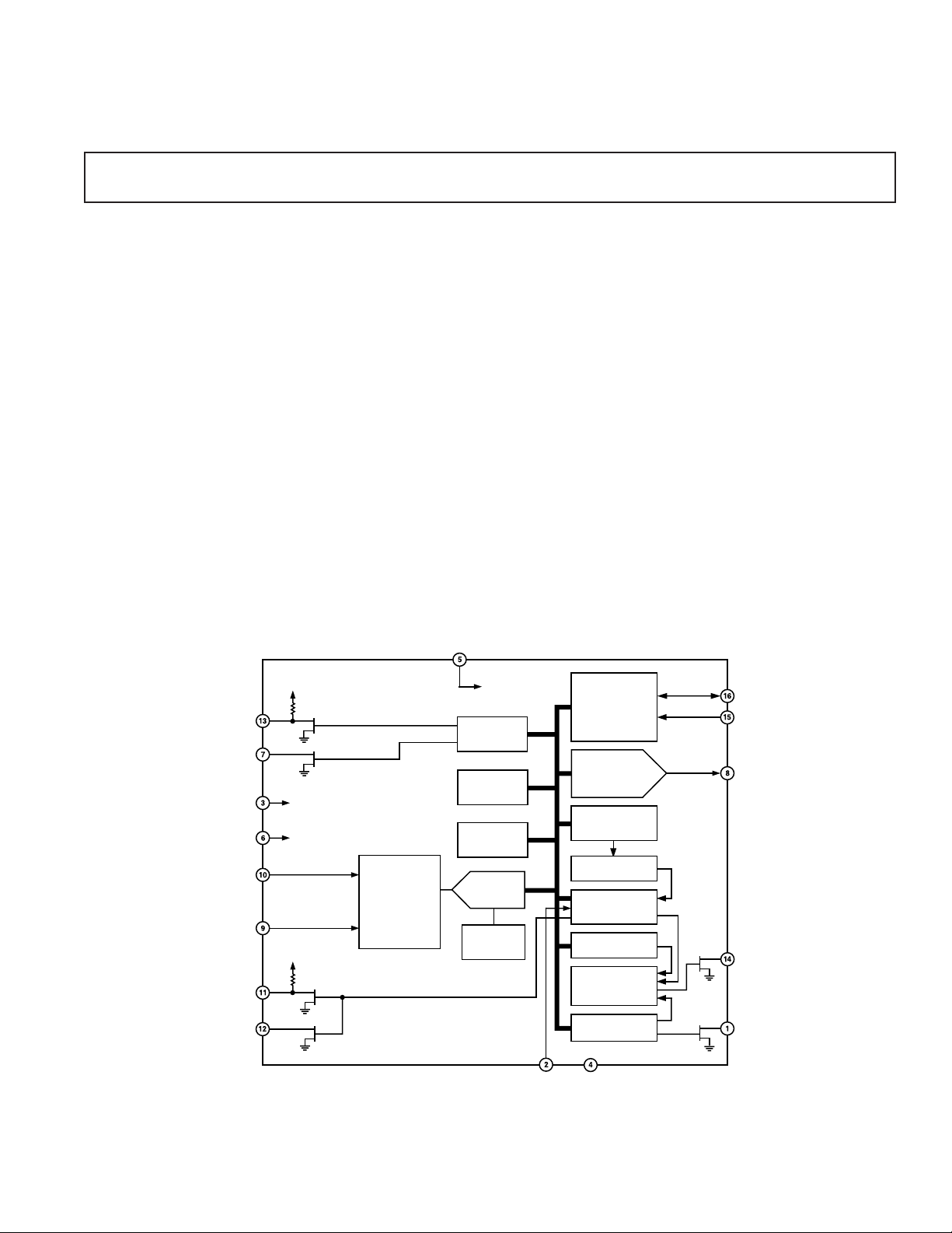
FUNCTIONAL BLOCK DIAGRAM
V
CC3AUX
V
CC3AUX
10k⍀
RESET
FAN_SPD SHUTOFF
AND R_OFF RESET
D+
D–
V
CC3AUX
10k⍀
ADM1028
ANALOG
SIGNAL
CONDITIONING
POWER-ON
RESET
REMOTE
FUNCTION
REGISTER
ADDRESS
POINTER
REGISTER
ALERT
STATUS
REGISTER
ADC
2.5V
BANDGAP
REFERENCE
SERIAL BUS
INTERFACE
ANALOG O/P
REGISTER,
COUNTER
AND 8-BIT DAC
VALUE AND
LIMIT
REGISTERS
LIMIT
COMPARATORS
INTERRUPT
STATUS
REGISTERS
INT MASK
REGISTER
MASK
GATING
CONFIGURATION
REGISTER
SDA
SCL
FAN_SPD/NTEST_IN
INT
FAN_OFF
REV. B
Information furnished by Analog Devices is believed to be accurate and
reliable. However, no responsibility is assumed by Analog Devices for its
use, nor for any infringements of patents or other rights of third parties that
may result from its use. No license is granted by implication or otherwise
under any patent or patent rights of Analog Devices. Trademarks and
registered trademarks are the property of their respective companies.
GPI
GND
One Technology Way, P.O. Box 9106, Norwood, MA 02062-9106, U.S.A.
Tel: 781/329-4700 www.analog.com
Fax: 781/326-8703 © 2003 Analog Devices, Inc. All rights reserved.

1, 2
ADM1028–SPECIFICATIONS
(TA = T
Parameter Min Typ Max Unit Test Conditions
POWER SUPPLY
Supply Voltage, V
Supply Current, I
CC
CC
3.0 3.30 5.5 V
TEMPERATURE-TO-DIGITAL CONVERTER
Internal Sensor Accuracy ± 3 ∞C
Resolution 1 ∞C
External Diode Sensor Accuracy ± 5 ∞C
Resolution 1 ∞C
Remote Sensor Source Current 120 mAHigh Level (D+ = D– + 0.65 V)
ANALOG OUTPUT
Output Voltage Range 0 2.5 V
Total Unadjusted Error, TUE ± 3%I
Full-Scale Error ± 1 ± 3%
Zero Error ± 2 LSB No Load
Differential Nonlinearity, DNL ± 1 LSB Monotonic by Design
Integral Nonlinearity ± 1 LSB
Output Source Current 2 mA
Output Sink Current 1 mA
THERMA OUTPUT
THERMA Pull-Up Resistance 9 12 14 kW
DIGITAL OUTPUT THERMA/NTEST_OUT,
R_OFF
Output High Voltage, V
Output Low Voltage, V
OL
OH
2.4 V I
OPEN-DRAIN DIGITAL OUTPUTS
(INT, THERMB, FAN_OFF, R_RST)
Output Low Voltage, V
High Level Output Leakage Current, I
OL
OH
FAN SPEED RAMP RATES
Counter Frequency 1 ± 50% 16 ± 50% Hz
OPEN-DRAIN SERIAL DATA
BUS OUTPUT (SDA)
Output Low Voltage, V
High Level Output Leakage Current, I
OL
OH
SERIAL BUS DIGITAL INPUTS
(SCL, SDA)
Input High Voltage, V
Input Low Voltage, V
IL
IH
2.1 V
Input Leakage Current ±5 mA
Hysteresis 500 mV Note 4
DIGITAL INPUT LOGIC LEVELS
(FAN_SPD/TEST_IN, GPI)
Input High Voltage, V
Input Low Voltage, V
IL
IH
2.2 V
DIGITAL INPUT LEAKAGE CURRENT
(ALL DIGITAL INPUTS)
Input High Current, I
Input Low Current, I
Input Capacitance, C
IL
IN
IH
–1 –0.005 mAV
369 pF Note 4
to T
MIN
, VCC = V
MAX
MIN
to V
, unless otherwise noted.)
MAX
2 3.2 mA Interface Inactive, ADC Active
± 2 ∞C60∞C £ T
± 3 ∞C60∞C £ T
£ 100∞C
A
£ 100∞C
A
7 mALow Level (D+ = D– + 0.65 V)
= 2 mA
L
= 3.0 mA
OUT
0.4 V
0.4 V I
0.1 1 mAV
0.4 V I
0.1 1 mAV
= –3.0 mA
OUT
= V
OUT
= –3.0 mA
OUT
= V
OUT
CC
CC
3
0.8 V
0.8 V
= V
IN
+0.005 +1 mAV
IN
CC
= 0
–2–
REV. B

Parameter Min Typ Max Unit Test Conditions
SCLK
BUF
SU;STA
HD;STA
LOW
HIGH
SU;DAT
HD;DAT
4
100 kHz See Figure 1
4.7 ms See Figure 1
4.7 ms See Figure 1
4.0 ms See Figure 1
SU;STO
4.0 ms See Figure 1
4.7 ms See Figure 1
4.0 ms See Figure 1
r
f
1000 ns See Figure 1
300 ns See Figure 1
250 ns See Figure 1
300 ns See Figure 1
= 0.8 V for a falling edge and V
IL
= 2.2 V for a rising edge.
IH
SERIAL BUS TIMING
Clock Frequency, f
Bus Free Time, t
Start Setup Time, t
Start Hold Time, t
Stop Condition Setup Time, t
SCL Low Time, t
SCL High Time, t
SCL, SDA Rise Time, t
SCL, SDA Fall Time, t
Data Setup Time, t
Data Hold Time, t
NOTES
1
Typicals are at TA = 25∞C and represent most likely parametric norm. Standby current typ is measured with VCC = 3.3 V.
2
Timing specifications are tested at logic levels of V
3
IOH for FAN_OFF guaranteed by design, not production tested.
4
Guaranteed by design, not production tested.
Specifications subject to change without notice.
ADM1028
ABSOLUTE MAXIMUM RATINGS
*
Positive Supply Voltage (VCC) . . . . . . . . . . . . . . . . . . . . . 6.5 V
Voltage on Digital Inputs Except Therm
and D– . . . . . . . . . . . . . . . . . . . . . . . . . . . . –0.3 V to +6.5 V
Voltage on Therm Pin . . . . . . . . . . . . . . –0.3 V to V
+ 0.3 V
CC
Voltage on D– Pin . . . . . . . . . . . . . . . . . . . . –0.3 V to + 0.6 V
Voltage on Any Other Input . . . . . . . . . –0.3 V to V
+ 0.3 V
CC
or Output Pin
Input Current at Any Pin . . . . . . . . . . . . . . . . . . . . . . . ± 5 mA
Package Input Current . . . . . . . . . . . . . . . . . . . . . . . ± 20 mA
Maximum Junction Temperature (T
max) . . . . . . . . . . 150∞C
J
Storage Temperature Range . . . . . . . . . . . . –65∞C to +150∞C
Lead Temperatures
Soldering (10 sec) . . . . . . . . . . . . . . . . . . . . . . . . . . . 300∞C
IR Reflow Peak Temperature . . . . . . . . . . . . . . . . . . . 220∞C
ESD Rating (Human Body Model) . . . . . . . . . . . . . . . 4000 V
*Stresses above those listed under Absolute Maximum Ratings may cause perma-
nent damage to the device. This is a stress rating only; functional. Operation of the
device at these or any other conditions above those indicated in the operational
section of this specification is not implied. Exposure to absolute maximum rating
conditions for extended periods may affect device reliability.
t
t
F
HIGH
SCL
t
LOW
t
HD; STA
t
R
t
HD; DAT
THERMAL CHARACTERISTICS
16-Lead QSOP Package:
= 105∞C/W, qJC = 39∞C/W
q
JA
ORDERING GUIDE
Temperature Package Package
Model Range Description Option
ADM1028ARQ 0∞C to 100∞C Shrink Small Outline RQ-16
Package (QSOP)
t
HD; STA
t
SU; DAT
t
SU; STA
t
SU; STO
SDA
t
BUF
PS
S
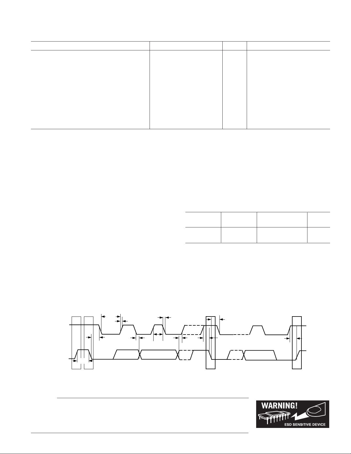
Figure 1. Serial Bus Timing Diagram
CAUTION
ESD (electrostatic discharge) sensitive device. Electrostatic charges as high as 4000 V readily
accumulate on the human body and test equipment and can discharge without detection.
Although the ADM1028 features proprietary ESD protection circuitry, permanent damage may
occur on devices subjected to high energy electrostatic discharges. Therefore, proper ESD
precautions are recommended to avoid performance degradation or loss of functionality.
REV. B
–3–
P

ADM1028
PIN CONFIGURATION
FAN_OFF
GPI
AUXRST
GND
V
CC3AUX
RST
R_RST
FAN_SPD/NTEST_IN
1
2
3
ADM1028
4
TOP VIEW
5
(Not to Scale)
6
7
8
16
SDA
15
SCL
14
INT
13
R_OFF
12
THERMB
11
THERMA/NTEST_OUT
10
D+
9
D–
PIN FUNCTION DESCRIPTIONS
Pin No. Mnemonic Description
1 FAN_OFF Digital Output (Open Drain) Fan Off Request. When asserted low, this indicates a
request to shut off the fan independent of the FAN_SPD output. When negated (output
FET off) it indicates that the fan may be turned on.
2 GPI Digital Input (12 V tolerant). This pin is a general-purpose logic input with 12 V toler-
ance. It can be programmed as an active high or active low input that sets Bit 4 of the
Interrupt Status Register. A voltage >2.2 V on this pin, represents a Logic “1,” while a
floating condition is interpreted as Logic “0.”
3 AUXRST Digital Input. This pin can be driven low as an input to reset the ADM1028.
4GND Ground. Power and signal ground.
5V
CC3AUX
Power 3.3 V Aux. Power source and voltage monitor input for power-on reset.
6 RST Digital Input. This pin can be pulled low externally to indicate to the ADM1028 that the
main system power has been removed. The ADM1028 will shut off the FAN_SPD output and reset its R_OFF output.
7 R_RST Digital Output (Open Drain). This pin is a remote reset output that pulses low on
receipt of a specific SMBus message.
8 FAN_SPD/NTEST_IN Analog Output/Test Input. An active-high input that enables NAND board-level
connectivity testing. Refer to section on NAND testing.
Used as an analog output for fan speed control when NAND test is not selected.
9D–Remote Thermal Diode Negative Input. This is the negative input (current sink) from
the remote thermal diode. This also serves as the negative input into the A/D.
10 D+ Remote Thermal Diode Positive Input. This is the positive input (current source) from
the remote thermal diode. This serves as the positive input into the A/D.
11 THERMA/NTEST_OUT Digital Output (Open Drain with Integrated V
Pull-Up). An active low thermal
CC3AUX
overload output that indicates a violation of a temperature setpoint (over temperature).
The fan is on full-speed whenever this pin is asserted low. Acts as the output of the NAND
Tree when the ADM1028 is in NAND Tree Test Mode.
12 THERMB Digital Output (Open Drain). This pin is a second THERM signal. It can be used to
drive external circuitry with a different external pull-up supply rail.
13 R_OFF Digital Output or Open Drain with Integrated V
Pull-Up. Remote off (power-
CC3AUX
down) output. This pin is driven high on receipt of a specific SMBus message. The pin
(and its associated register bit) remain high until the RST input is asserted low.
14 INT Digital Output (Open Drain), System Interrupt Output. This signal indicates a violation
of a set trip point. The output is enabled when Bit 1 of the Configuration Register is set
to 1. The default state is disabled.
15 SCL Digital Input. SMBus Clock.
16 SDA Digital I/O (Open Drain). SMBus Bidirectional Data.
–4–
REV. B

Typical Performance Characteristics–ADM1028
TEMPERATURE – ⴗC
4
ERROR – ⴗC
–3
0102030405060708090
–5
–4
–2
–1
0
1
2
3
100
LOWER SPEC LEVEL
UPPER SPEC LEVEL
SCLK FREQUENCY – kHz
SUPPLY CURRENT – mA
1.77
151025 50 75 100
1.67
1.72
1.82
1.87
1.92
1.97
2.02
250 500 750 1000
VDD = 5V
VDD = 3.3V
30
20
10
0
–10
TEMPERATURE ERROR – ⴗC
–20
–30
1
D+ TO GND
D+ TO V
DD
LEAKAGE RESISTANCE – M⍀
10 100
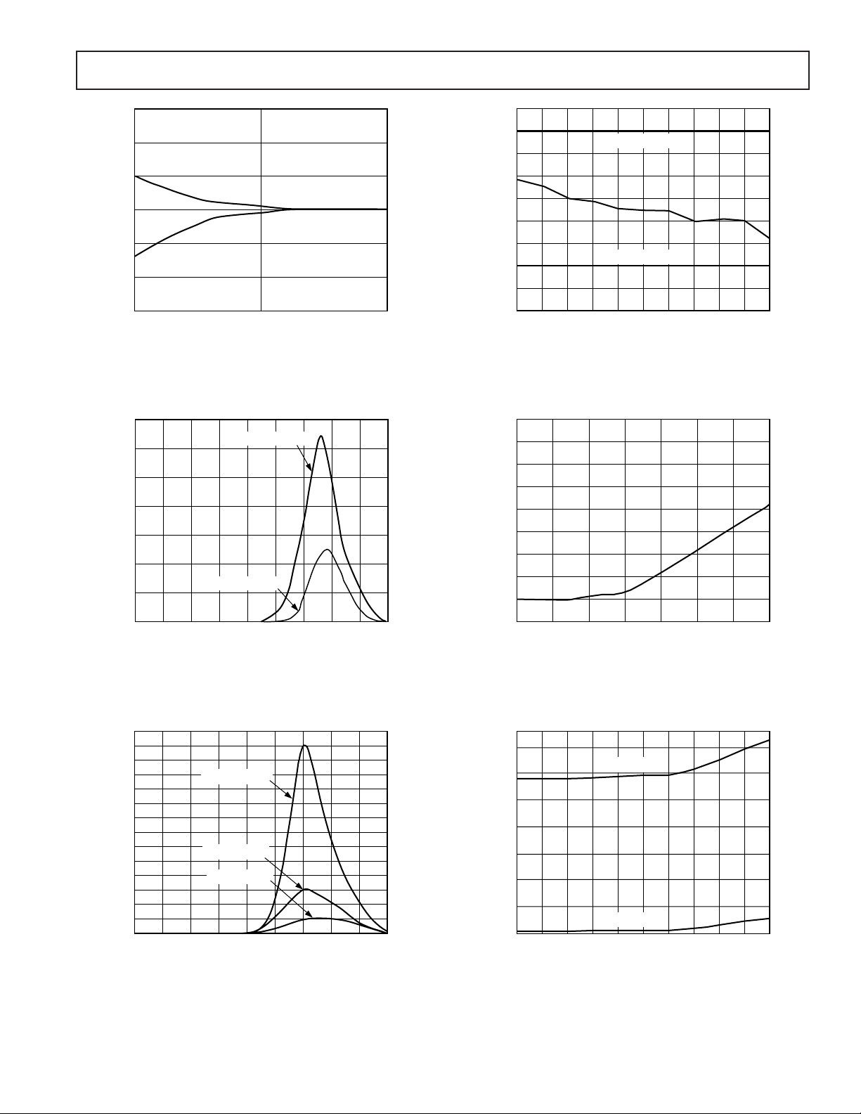
TPC 1. Temperature Error vs. PC Board Track Resistance
(D+ to V
)
DD
14
12
10
8
6
4
TEMPERATURE ERROR – ⴗC
2
0
1
10 100k 1000M
VIN = 250mV p-p
= 100mV p-p
V
IN
10k 100M1k 10M100 1M
FREQUENCY – Hz
TPC 2. Temperature Error vs. Power Supply
Noise Frequency
TPC 4. Temperature Error of ADM1028 vs. Pentium® III
Temperature
40
35
30
25
20
15
10
TEMPERATURE ERROR – ⴗC
5
0
–5
010203040506070
CAPACITANCE – nF
TPC 5. Temperature Error vs. Capacitance Between
D+ and D–
14
13
12
11
10
9
8
7
6
5
REV. B
4
3
TEMPERATURE ERROR – ⴗC
2
1
0
110100 1k 10k 100k 1M 10M 100M 1G
TPC 3. Temperature Error vs. Common-Mode
Noise Frequency
VIN = 100mV p-p
VIN = 50mV p-p
VIN = 25mV p-p
FREQUENCY – Hz
TPC 6. Standby Current vs. Clock Frequency
–5–
 Loading...