

Page 1
查询ADM1025供应商查询ADM1025供应商
Low-Cost PC
a
FEATURES
Up to Eight Measurement Channels
Five Inputs to Measure Supply Voltages
Monitored Internally
V
CC
External Temperature Measurement with Remote Diode
On-Chip Temperature Sensor
Five Digital Inputs for VID Bits
Integrated 100 k⍀ Pull-Ups on VID Pins (ADM1025 Only)
LDCM Support
2C®
-Compatible System Management Bus (SMBus)
I
Programmable RESET Output Pin
Programmable INT Output Pin
Configurable Offset for Internal/External Channel
Shutdown Mode to Minimize Power Consumption
Limit Comparison of all Monitored Values
APPLICATIONS
Network Servers and Personal Computers
Microprocessor-Based Office Equipment
Test Equipment and Measuring Instruments
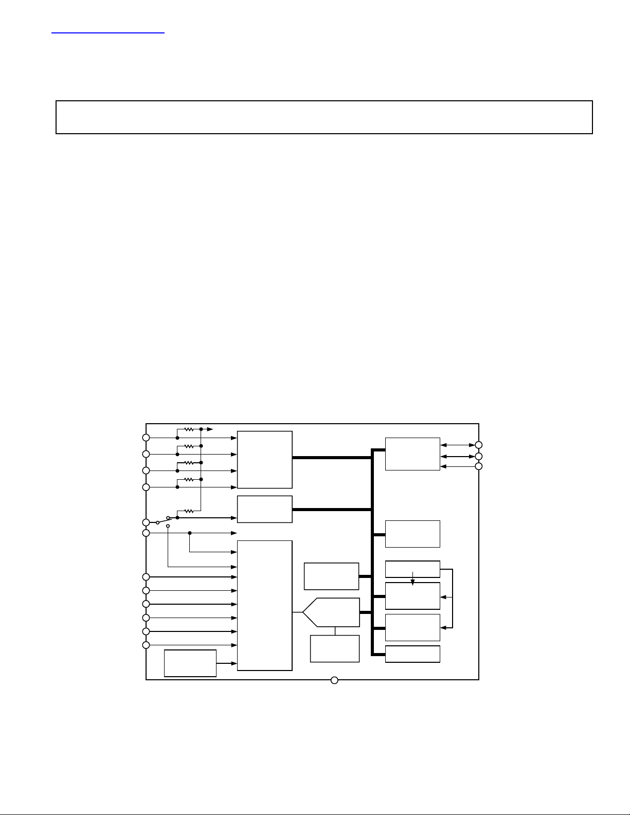
FUNCTIONAL BLOCK DIAGRAM
Hardware Monitor ASIC
ADM1025/ADM1025A*
PRODUCT DESCRIPTION
The ADM1025/ADM1025A is a complete system hardware
monitor for microprocessor-based systems, providing measurement and limit comparison of various system parameters. Five
voltage measurement inputs are provided, for monitoring 2.5 V,
3.3 V, 5 V and 12 V power supplies and the processor core
voltage. The ADM1025/ADM1025A can monitor a sixth power
supply voltage by measuring its own V
dedicated to a remote temperature-sensing diode, and an on-chip
temperature sensor allows ambient temperature to be monitored. The ADM1025A has open-drain VID inputs while the
ADM1025 has on-chip 100 kΩ pull-ups on the VID inputs.
Measured values and in/out of limit status can be read out via
2
an I
C-compatible serial System Management Bus. The device
can be controlled and configured over the same serial bus. The
device also has a programmable INT output to indicate undervoltage, overvoltage and over-temperature conditions.
The ADM1025/ADM1025A’s 3.0 V to 5.5 V supply voltage
range, low supply current, and I
it ideal for a wide range of applications. These include hardware
monitoring and protection applications in personal computers,
electronic test equipment, and office electronics.
. One input (two pins) is
CC
2
C-compatible interface make
V
VID0
VID1
VID2
VID3
300k⍀
/VID4
12V
IN
V
CC
V
CCPIN
2.5V
IN
3.3V
IN
5V
IN
D+
D–/NTI
BANDGAP
TEMPERATURE
SENSOR
*Patent Pending.
I2C is a registered trademark of Philips Corporation.
DD
100k⍀
PULLUPS
VID0–3
REGISTER
VID4
REGISTER
POWER TO CHIP
INPUT
ATTENUATORS
AND
ANALOG
MULTIPLEXER
REV. A
Information furnished by Analog Devices is believed to be accurate and
reliable. However, no responsibility is assumed by Analog Devices for its
use, nor for any infringements of patents or other rights of third parties
which may result from its use. No license is granted by implication or
otherwise under any patent or patent rights of Analog Devices.
SERIAL BUS
INTERFACE
ADD/RST/INT/NTO
SDA
SCL
ADM1025/
ADM1025A
VALUE AND
LIMIT
REGISTERS
ADDRESS
POINTER
REGISTER
ADC
2.5V
BANDGAP
REFERENCE
GND
One Technology Way, P.O. Box 9106, Norwood, MA 02062-9106, U.S.A.
Tel: 781/329-4700 World Wide Web Site: http://www.analog.com
Fax: 781/326-8703 © Analog Devices, Inc., 2000
LIMIT
COMPARATORS
MEASUREMENT
STATUS
REGISTERS
OFFSET
REGISTER
CONFIGURATION
REGISTER
Page 2

ADM1025/ADM1025A–SPECIFICATIONS
P
arameter Min Typ Max Unit Test Conditions/Comments
(TA = T
MIN
to T
, VCC = V
MAX
MIN
to V
, unless otherwise noted.)
MAX
POWER SUPPLY
Supply Voltage, V
Supply Current, I
CC
CC
3.0 3.30 5.5 V (Note 1)
1.4 2.5 mA Interface Inactive, ADC Active
32 500 µA Standby Mode (Note 2)
TEMPERATURE-TO-DIGITAL CONVERTER
Internal Sensor Accuracy ± 3 °C
Resolution 1 °C
External Diode Sensor Accuracy ± 5 °C
± 3 °C60°C ≤ T
≤ 100°C; VCC = 3.3 V
A
Resolution 1 °C
Remote Sensor Source Current 180 µA High Level
11 µA Low Level
ANALOG-TO-DIGITAL CONVERTER
(INCLUDING MUX AND ATTENUATORS)
Total Unadjusted Error, TUE ±2 % (Note 3)
Differential Nonlinearity, DNL ± 1 LSB
Power Supply Sensitivity ± 1 %/V
Conversion Time (Analog Input or Internal Temperature) 11.6 ms (Note 4)
Conversion Time (External Temperature) 34.8 ms (Note 4)
Input Resistance (2.5 V, 3.3 V, 5 V, 12 V, V
) 100 140 250 kΩ
CCPIN
OPEN-DRAIN DIGITAL OUTPUT ADD/RST/INT/NTO
Output Low Voltage, V
High Level Output Leakage Current, I
OL
OH
0.1 1 µAV
0.4 V I
= –6.0 mA; V
OUT
= VCC; V
OUT
CC
= 3 V
CC
= 3 V
RST Pulsewidth 20 45 ms
OPEN-DRAIN SERIAL DATA BUS OUTPUT (SDA)
Output Low Voltage, V
High Level Output Leakage Current, I
OL
OH
0.1 1 µAV
0.4 V I
= –6.0 mA; VCC = 3 V
OUT
= V
OUT
CC
SERIAL BUS DIGITAL INPUTS (SCL, SDA)
Input High Voltage, V
Input Low Voltage, V
IL
IH
2.1 V
0.8 V
Hysteresis 500 mV
DIGITAL INPUT LOGIC LEVELS
(ADD, VID0–VID4, NTI)
5
VID0–3 Input Resistance 100 kΩ ADM1025 Only
VID4 Input Resistance 300 kΩ ADM1025 Only
100 kΩ ADM1025A
2.1 V
0.8 V
Input High Voltage, V
Input Low Voltage, V
6
IH
6
IL
DIGITAL INPUT LEAKAGE CURRENT
Input High Current, I
Input Low Current, I
IL
Input Capacitance, C
IH
IN
–1 µAV
1 µAV
IN
IN
= V
= 0
CC
5pF
SERIAL BUS TIMING
Clock Frequency, f
Glitch Immunity, t
Bus Free Time, t
Start Setup Time, t
Start Hold Time, t
Stop Condition Setup Time t
SCL Low Time, t
SCL High Time, t
SCL, SDA Rise Time, t
SCL, SDA Fall Time, t
Data Setup Time, t
Data Hold Time, t
NOTES
1
All voltages are measured with respect to GND, unless otherwise specified.
2
Typicals are at TA = 25°C and represent most likely parametric norm. Shutdown current typ is measured with VCC = 3.3 V.
3
TUE (Total Unadjusted Error) includes Offset, Gain and Linearity errors of the ADC, multiplexer and on-chip input attenuators, including an external series input
protection resistor value between zero and 1 kΩ.
4
Total monitoring cycle time is nominally 114.4 ms. Monitoring Cycle consists of 6 Voltage + 1 Internal Temperature + 1 External Temperature readings.
5
ADD is a three-state input that may be pulled high, low or left open-circuit.
6
Timing specifications are tested at logic levels of V
Specifications subject to change without notice.
SCLK
SW
BUF
SU:STA
HD:STA
LOW
HIGH
SU:DAT
HD:DAT
50 ns See Figure 1
1.3 µs See Figure 1
600 ns See Figure 1
600 ns See Figure 1
SU:STO
600 ns See Figure 1
1.3 µs See Figure 1
0.6 µs See Figure 1
R
F
100 ns See Figure 1
300 ns See Figure 1
= 0.8 V for a falling edge and V
IL
= 2.2 V for a rising edge.
IH
400 kHz See Figure 1
300 ns See Figure 1
300 ns See Figure 1
–2–
REV. A
Page 3
ADM1025/ADM1025A
ABSOLUTE MAXIMUM RATINGS*
Positive Supply Voltage (VCC) . . . . . . . . . . . . . . . . . . . . .6.5 V
Voltage on 12 V V
Pin . . . . . . . . . . . . . . . . . . . . . . . . . 20 V
IN
Voltage on Any Input or Output Pin . . . . . . . . . –0.3 V to +6.5 V
Input Current at Any Pin . . . . . . . . . . . . . . . . . . . . . . . ± 5 mA
Package Input Current . . . . . . . . . . . . . . . . . . . . . . . ± 20 mA
Maximum Junction Temperature (TJ max) . . . . . . . . . . 150°C
Storage Temperature Range . . . . . . . . . . . . –65°C to +150°C
Lead Temperature, Soldering
Vapor Phase 60 sec . . . . . . . . . . . . . . . . . . . . . . . . . . . 215°C
Infrared 15 sec . . . . . . . . . . . . . . . . . . . . . . . . . . . . . . 200°C
ESD Rating All Pins . . . . . . . . . . . . . . . . . . . . . . . . . . 2000 V
ORDERING GUIDE
Temperature Package Package
Model Range Description Option Option
ADM1025ARQ 0°C to 100°C 16-Lead QSOP RQ-16 Integrated 100
ADM1025AARQ 0°C to 100°C 16-Lead QSOP RQ-16 Open-Drain VID Inputs
t
LOW
t
R
t
F
*Stresses above those listed under Absolute Maximum Ratings may cause perma-
nent damage to the device. This is a stress rating only; functional operation of the
device at these or any other conditions above those indicated in the operational
section of this specification is not implied. Exposure to absolute maximum rating
conditions for extended periods may affect device reliability.
THERMAL CHARACTERISTICS
16-Lead QSOP Package:
θ
= 105°C/W
JA
= 39°C/W
θ
JC
kΩ
VID Pull-Ups
t
HD:STA
SCL
SDA
t
t
HD:STA
t
BUF
S
HD:DAT
t
HIGH
t
SU:DAT
t
SU:STA
t
HD:STO
PSP
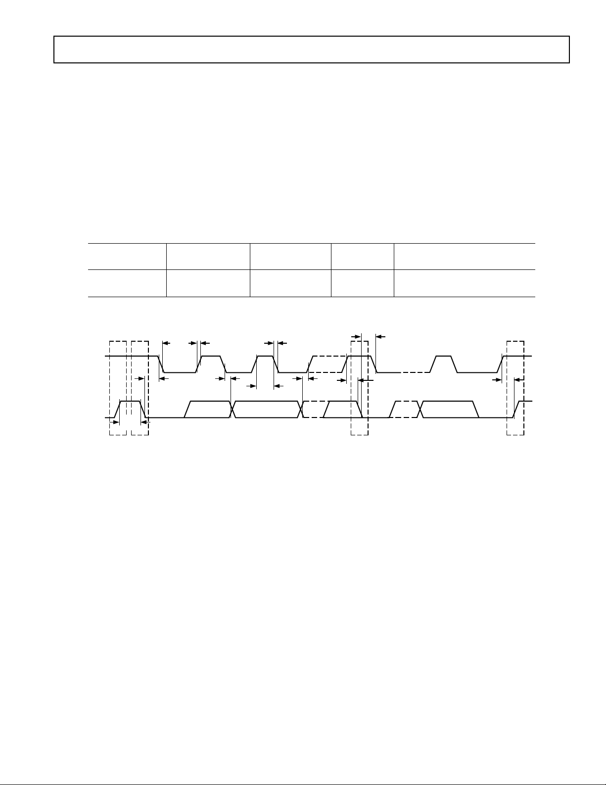
Figure 1. Diagram for Serial Bus Timing
REV. A
–3–
Page 4

ADM1025/ADM1025A
PIN FUNCTION DESCRIPTIONS
Pin
No. Mnemonic Description
1 SDA Digital I/O. Serial bus bidirectional data. Open-drain output.
2 SCL Digital Input. Serial bus clock.
3 GND System Ground.
4V
CC
5 VID0 Digital Input. Core voltage ID readouts from the processor. This value is read into the VID0–VID3
6 VID1 Digital Input. Core voltage ID readouts from the processor. This value is read into the VID0–VID3
7 VID2 Digital Input. Core voltage ID readouts from the processor. This value is read into the VID0–VID3
8 VID3 Digital Input. Core voltage ID readouts from the processor. This value is read into the VID0–VID3
9 D–/NTI Analog/Digital Input. Connected to cathode of external temperature sensing diode. If held high at
10 D+ Analog Input. Connected to anode of external temperature sensing diode.
11 12 V
12 5 V
13 3.3 V
14 2.5 V
15 V
/VID4 Programmable Analog/Digital Input. Defaults to 12 VIN analog input at power-up, but may be pro-
IN
IN
IN
IN
CCPIN
16 ADD/RST/INT/NTO Programmable Digital I/O. The lowest order programmable bit of the SMBus Address, sampled on
Power. Can be powered by +3.3 V standby power if monitoring in low power states is required.
This pin also serves as the analog input to monitor V
CC
.
Status Register. It has an on-chip 100 kΩ pull-up resistor (ADM1025 only).
Status Register. It has an on-chip 100 kΩ pull-up resistor (ADM1025 only).
Status Register. It has an on-chip 100 kΩ pull-up resistor (ADM1025 only).
Status Register. It has an on-chip 100 kΩ pull-up resistor (ADM1025 only).
power-up, initiates NAND tree test mode.
grammed as VID4 Core Voltage ID readout from the processor. This value is read into the VID4
Status Register. In analog 12 V
mode it has an on-chip voltage attenuator. In VID4 mode it has an
IN
on-chip 300 kΩ pull-up resistor.
Analog Input. Monitors 5 V supply.
Analog Input. Monitors 3.3 V supply.
Analog Input. Monitors 2.5 V supply.
Analog Input. Monitors processor core voltage (0 V to 3.0 V).
SMB activity as a three-state input. Can also be configured to give a minimum 20 ms low reset
output pulse. Alternatively, can be programmed as an interrupt output for temperature/voltage
interrupts. Functions as the output of the NAND tree in NAND tree test mode.
PIN CONFIGURATION
SDA
SCL
GND
V
VID0
VID1
VID2
VID3
1
2
3
4
CC
5
6
7
8
ADM1025/
ADM1025A
TOP VIEW
(Not to Scale)
16
ADD/RST/INT/NTO
V
15
CCPIN
2.5V
14
IN
3.3V
13
IN
5V
12
IN
12V
/VID4
11
IN
10
D+
D–/NTI
9
–4–
REV. A
Page 5
Typical Performance Characteristics–
ADM1025/ADM1025A
30
20
10
0
–10
–20
–30
TEMPERATURE ERROR – ⴗC
–40
–50
–60
1 1003.3
LEAKAGE RESISTANCE – M⍀
DXP TO GND
DXP TO VCC (5V)
10 30
Figure 2. Temperature Error vs. PC Board Track Resistance
6
5
4
250mV p-p REMOTE
3
2
1
TEMPERATURE ERROR – ⴗC
0
100mV p-p REMOTE
120
100
90
80
70
60
50
READING
40
30
20
10
0
0 11010
20 30 40 50
MEASURED TEMPERATURE
60 70 80 90 100
Figure 5. Pentium II® Temperature Measurement vs.
ADM1025/ADM1025A Reading
25
20
15
10
5
TEMPERATURE ERROR – ⴗC
0
–1
50 50M500
5k
50k
FREQUENCY – Hz
500k 5M
Figure 3. Temperature Error vs. Power Supply Noise
Frequency
25
20
15
10
5
TEMPERATURE ERROR – ⴗC
0
–5
50 50M500
5k 50k 500k 5M
FREQUENCY – Hz
100mV p-p
50mV p-p
25mV p-p
Figure 4. Temperature Error vs. Common-Mode Noise
Frequency
–5
1102.2
3.2 4.7 7
DXP-DXN CAPACITANCE – nF
Figure 6. Temperature Error vs. Capacitance Between D+
and D–
10
9
8
TEMPERATURE ERROR – ⴗC
7
6
5
4
3
2
1
0
50 50M500
5k 50k 500k 5M
10mV SQ. WAVE
100k 25M
FREQUENCY – Hz
Figure 7. Temperature Error vs. Differential-Mode Noise
Frequency
Pentium II is a registered trademark of Intel Corporation.
REV. A
–5–
Page 6

ADM1025/ADM1025A
26.5
26.0
SHUTDOWN CURRENT – A
25.5
25.0
24.5
24.0
23.5
23.0
22.5
–40 –20
VDD = 3.3V
0 20 40 60 80 100 120
TEMPERATURE – C
Figure 8. Standby Current vs. Temperature
GENERAL DESCRIPTION
The ADM1025/ADM1025A is a complete system hardware
monitor for microprocessor-based systems. The device communicates with the system via a serial System Management Bus.
The serial bus controller has a hardwired address line for device
selection (Pin 16), a serial data line for reading and writing
addresses and data (Pin 1), and an input line for the serial clock
(Pin 2). All control and programming functions of the ADM1025/
ADM1025A are performed over the serial bus.
MEASUREMENT INPUTS
The device has six measurement inputs, five for voltage and one
for temperature. It can also measure its own supply voltage and
can measure ambient temperature with its on-chip temperature
sensor.
Pins 11 through 15 are analog inputs with on-chip attenuators,
configured to monitor 12 V, 5 V, 3.3 V, 2.5 V and the processor
core voltage, respectively. Pin 11 may alternatively be programmed
as a digital input for Bit 4 of the processor voltage ID code.
Power is supplied to the chip via Pin 4 and the system also
monitors the voltage on this pin.
Remote temperature sensing is provided by the D+ and D–
inputs, to which a diode-connected, external temperaturesensing transistor may be connected.
An on-chip bandgap temperature sensor monitors system ambient temperature.
SEQUENTIAL MEASUREMENT
When the ADM1025/ADM1025A monitoring sequence is started,
it cycles sequentially through the measurement of analog inputs
and the temperature sensors. Measured values from these inputs
are stored in Value Registers. These can be read out over the
serial bus, or can be compared with programmed limits stored
in the Limit Registers. The results of out-of-limit comparisons
are stored in the Status Registers, which can be read over the
serial bus to flag out of limit conditions.
PROCESSOR VOLTAGE ID
Five digital inputs (VID4 to VID0—Pins 5 to 8 and 11) read the
processor voltage ID code and store it in the VID registers, from
which it can be read out by the management system over the
serial bus. If Pin 11 is configured as a 12 V analog input (powerup default), the VID4 bit in the VID4 register will default to 0.
The VID pins have internal 100 kΩ pull-up resistors (ADM1025
only).
ADD/RST/INT/NTO
Pin 16 is a programmable digital I/O pin. After power-up, at the
first sign of SMBus activity, it is sampled to set the lowest two
bits of the serial bus address. During board-level, NAND tree
connectivity testing, this pin functions as the output of the NAND
tree. During normal operation Pin 16 may be programmed as a
reset output to provide a low going 20 ms reset pulse when
enabled, or it may be programmed as an interrupt output for
out-of-limit temperature and/or voltage events. These functions
are described in more detail later.
INTERNAL REGISTERS OF THE ADM1025/ADM1025A
A brief description of the ADM1025/ADM1025A’s principal
internal registers is given below. More detailed information on
the function of each register is given in Tables V to XV.
Configuration Register: Provides control and configuration.
Address Pointer Register: This register contains the address that
selects one of the other internal registers. When writing to the
ADM1025/ADM1025A, the first byte of data is always a register
address, which is written to the Address Pointer Register.
Status Registers: Two registers to provide status of each limit
comparison.
VID Registers: The status of the VID0 to VID4 pins of the
processor can read from these registers.
Value and Limit Registers: The results of analog voltage
inputs and temperature measurements are stored in these registers, along with their limit values.
Offset Register: Allows either an internal or external temperature channel reading to be offset by a two’s complement value
written to this register.
SERIAL BUS INTERFACE
Control of the ADM1025/ADM1025A is carried out via the
serial bus. The ADM1025/ADM1025A is connected to this
bus as a slave device, under the control of a master device or
master controller.
The ADM1025/ADM1025A has a 7-bit serial bus address. When
the device is powered up, it will do so with a default serial bus
address. The five MSBs of the address are set to 01011, the two
LSBs are determined by the logical states of Pin 16 at power-up.
This is a three-state input that can be grounded, connected to
V
or left open-circuit to give three different addresses:
CC
Table I. Address Selection
–6–
ADD Pin A1 A0
GND 0 0
No Connect 1 0
V
CC
01
REV. A
Page 7

ADM1025/ADM1025A
If ADD is left open-circuit the default address will be 0101110.
ADD is sampled only after power-up, so any changes made will
have no effect, unless power is cycled.
The facility to make hardwired changes to A1 and A0 allows the
user to avoid conflicts with other devices sharing the same serial
bus if, for example, more than one ADM1025/ADM1025A is
used in a system. However, as previously mentioned, the ADD
pin may also function as a reset output or interrupt output. Use
of these functions may restrict the addresses that can be set. See
the sections on RST and INT for further information.
The serial bus protocol operates as follows:
1. The master initiates data transfer by establishing a START
condition, defined as a high-to-low transition on the serial
data line SDA while the serial clock line SCL remains high.
This indicates that an address/data stream will follow. All
slave peripherals connected to the serial bus respond to the
START condition, and shift in the next eight bits, consisting
of a 7-bit address (MSB first) plus an R/W bit, which determines the direction of the data transfer, i.e., whether data
will be written to or read from the slave device.
The peripheral whose address corresponds to the transmitted
address responds by pulling the data line low during the low
period before the ninth clock pulse, known as the Acknowledge Bit. All other devices on the bus now remain idle while
the selected device waits for data to be read from or written
to it. If the R/W bit is a 0, the master will write to the slave
device. If the R/W bit is a 1, the master will read from the
slave device.
2. Data is sent over the serial bus in sequences of nine clock
pulses, eight bits of data followed by an Acknowledge Bit
from the slave device. Transitions on the data line must
occur during the low period of the clock signal and remain
stable during the high period, as a low-to-high transition
when the clock is high may be interpreted as a STOP signal.
The number of data bytes that can be transmitted over the
serial bus in a single READ or WRITE operation is limited
only by what the master and slave devices can handle.
3. When all data bytes have been read or written, stop conditions are established. In WRITE mode, the master will pull
the data line high during the 10th clock pulse to assert a
STOP condition. In READ mode, the master device will
override the acknowledge bit by pulling the data line high
during the low period before the 9th clock pulse. This is
known as No Acknowledge. The master will then take the
data line low during the low period before the 10th clock
pulse, then high during the 10th clock pulse to assert a
STOP condition.
Any number of bytes of data may be transferred over the serial
bus in one operation, but it is not possible to mix read and write
in one operation, because the type of operation is determined at
the beginning and cannot subsequently be changed without
starting a new operation.
In the case of the ADM1025/ADM1025A, write operations
contain either one or two bytes, and read operations contain one
byte, and perform the following functions:
To write data to one of the device data registers or read data
from it, the Address Pointer Register must be set so that the
correct data register is addressed, data can then be written into
that register or read from it. The first byte of a write operation
always contains an address that is stored in the Address Pointer
Register. If data is to be written to the device, the write operation contains a second data byte that is written to the register
selected by the address pointer register.
This is illustrated in Figure 9a. The device address is sent over
the bus followed by R/W set to 0. This is followed by two data
bytes. The first data byte is the address of the internal data
register to be written to, which is stored in the Address Pointer
Register. The second data byte is the data to be written to the
internal data register.
SCL
SDA
START BY
MASTER
19
1 0 1 1 A1 A0 D7
FRAME 1
SERIAL BUS ADDRESS BYTE
SCL (CONTINUED)
SDA (CONTINUED)
R/W0
ADM1025
ACK. BY
1
D7 D6
1
D6
D5 D4 D3
D2
D2
D1 D0
D1
D5 D4 D3
ADDRESS POINTER REGISTER BYTE
FRAME 2
FRAME 3
DATA BYTE
ACK. BY
ADM1025
D0
9
9
ACK. BY
ADM1025
STOP BY
MASTER
Figure 9a. Writing a Register Address to the Address Pointer Register, then Writing Data to the Selected Register
REV. A
–7–
Page 8

ADM1025/ADM1025A
191
SCL
SDA 1 0 1 1 A1 A0 D7
START BY
MASTER
0
FRAME 1
SERIAL BUS ADDRESS BYTE
R/W
ACK. BY
ADM1025
Figure 9b. Writing to the Address Pointer Register Only
19
SCL
0
SDA
START BY
MASTER
1 0 1 1 A1 A0 D7
FRAME 1
SERIAL BUS ADDRESS BYTE
R/W
ACK. BY
ADM1025
Figure 9c. Reading Data from a Previously Selected Register
When reading data from a register there are two possibilities:
1. If the ADM1025/ADM1025A’s Address Pointer Register
value is unknown or not the desired value, it is first necessary
to set it to the correct value before data can be read from the
desired data register. This is done by performing a write to
the ADM1025/ADM1025A as before, but only the data byte
containing the register address is sent, as data is not to be
written to the register. This is shown in Figure 9b.
A read operation is then performed consisting of the serial bus
address, R/W bit set to 1, followed by the data byte read from
the data register. This is shown in Figure 9c.
2. If the Address Pointer Register is known to be already at the
desired address, data can be read from the corresponding
data register without first writing to the Address Pointer
Register, so Figure 9b can be omitted.
NOTES
1. Although it is possible to read a data byte from a data register
without first writing to the Address Pointer Register, if the
Address Pointer Register is already at the correct value, it is
not possible to write data to a register without writing to the
Address Pointer Register, because the first data byte of a
write is always written to the Address Pointer Register.
2. In Figures 9a to 9c, the serial bus address is shown as the
default value 01011(A1)(A0), where A1 and A0 are set by
the three-state ADD pin.
3. In addition to supporting the Send Byte and Receive Byte
protocols, the ADM1025/ADM1025A also supports the
Read Byte protocol (see System Management Bus specifications Rev. 1.1 for more information).
4. If Reset or Interrupt functionality is required, address pin
cannot be strapped to GND, as this would keep the ADD/
RST/INT/NTO pin permanently low.
MEASUREMENT INPUTS
The ADM1025/ADM1025A has six external measurement
inputs, five for voltage and one (two pins) for temperature.
Internal measurements are also carried out on V
and the
CC
on-chip temperature sensor.
–8–
9
D6
ADDRESS POINTER REGISTER BYTE
1
D6
D4
D5
FRAME 2
D5 D4 D3
FRAME 2
DATA BYTE FROM ADM1025
D3
D2
D2
D1
D1
D0
ACK. BY
ADM1025
D0
NO ACK.
BY MASTER
STOP BY
MASTER
9
STOP BY
MASTER
A-TO-D CONVERTER
These inputs are multiplexed into the on-chip, successive approximation, analog-to-digital converter. This has a resolution
of eight bits. The basic input range is zero to 2.5 V, but the
inputs have built-in attenuators to allow measurement of 2.5 V,
3.3 V, 5 V, 12 V and the processor core voltage V
, without
CCP
any external components. To allow for the tolerance of these
supply voltages, the A-to-D converter produces an output of
3/4 full scale (decimal 192) for the nominal input voltage, and
so has adequate headroom to cope with overvoltages. Table II
shows the input ranges of the analog inputs and output codes of
the A-to-D converter.
When the ADC is running, it samples and converts an input
every 11.6 ms, except for the external temperature (D+ and D–)
input. This has special input signal conditioning and is averaged
over 16 conversions to reduce noise; a measurement on this
input takes nominally 34.8 ms.
INPUT CIRCUITS
The internal structure for the analog inputs are shown in Figure
10. Each input circuit consists of an input protection diode, an
attenuator, plus a capacitor to form a first-order low-pass filter
which gives the input immunity to high frequency noise.
122.2k
12V
3.3V
2.5V
V
5V
CCPIN
IN
IN
IN
IN
22.7k
91.6k
55.2k
62.6k
82.4k
36.7k
111.2k
19.6k
105k⍀
⍀
⍀
⍀
⍀
⍀
⍀
⍀
⍀
⍀
35pF
25pF
25pF
25pF
10pF
MUX
Figure 10. Structure of Analog Inputs
REV. A
Page 9

ADM1025/ADM1025A
Table II. A/D Output Code vs. V
IN
Input Voltage A/D Output
12 V
IN
5 V
IN
VCC/3.3 V
IN
2.5 V
IN
V
CCPIN
Decimal Binary
<0.062 <0.026 <0.0172 <0.013 <0.012 0 0000 0000
0.062–0.125 0.026–0.052 0.017–0.034 0.013–0.026 0.012–0.023 1 0000 0001
0.125–0.188 0.052–0.078 0.034–0.052 0.026–0.039 0.023–0.035 2 0000 0010
0.188–0.250 0.078–0.104 0.052–0.069 0.039–0.052 0.035–0.047 3 0000 0011
0.250–0.313 0.104–0.130 0.069–0.086 0.052–0.065 0.047–0.058 4 0000 0100
0.313–0.375 0.130–0.156 0.086–0.103 0.065–0.078 0.058–0.070 5 0000 0101
0.375–0.438 0.156–0.182 0.103–0.120 0.078–0.091 0.070–0.082 6 0000 0110
0.438–0.500 0.182–0.208 0.120–0.138 0.091–0.104 0.082–0.093 7 0000 0111
0.500–0.563 0.208–0.234 0.138–0.155 0.104–0.117 0.093–0.105 8 0000 1000
•
•
•
4.000–4.063 1.666–1.692 1.100–1.117 0.833–0.846 0.749–0.761 64 (1/4 Scale) 0100 0000
•
•
•
8.000–8.063 3.330–3.560 2.200–2.217 1.667–1.680 1.499–1.511 128 (1/2 Scale) 1000 0000
•
•
•
12.000–12.063 5.000–5.026 3.300–3.317 2.500–2.513 2.249–2.261 192 (3/4 Scale) 1100 0000
•
•
•
15.312–15.375 6.380–6.406 4.210–4.230 3.190–3.203 2.869–2.881 245 1111 0101
15.375–15.437 6.406–6.432 4.230–4.245 3.203–3.216 2.881–2.893 246 1111 0110
15.437–15.500 6.432–6.458 4.245–4.263 3.216–3.229 2.893–2.905 247 1111 0111
15.500–15.563 6.458–6.484 4.263–4.280 3.229–3.242 2.905–2.916 248 1111 1000
15.625–15.625 6.484–6.510 4.280–4.300 3.242–3.255 2.916–2.928 249 1111 1001
15.625–15.688 6.510–6.536 4.300–4.314 3.255–3.268 2.928–2.940 250 1111 1010
15.688–15.750 6.536–6.562 4.314–4.330 3.268–3.281 2.940–2.951 251 1111 1011
15.750–15.812 6.562–6.588 4.331–4.348 3.281–3.294 2.951–2.964 252 1111 1100
15.812–15.875 6.588–6.615 4.348–4.366 3.294–3.307 2.964–2.975 253 1111 1101
15.875–15.938 6.615–6.640 4.366–4.383 3.307–3.320 2.975–2.987 254 1111 1110
>15.938 >6.640 >4.383 >3.320 >2.988 255 1111 1111
REV. A
–9–
Page 10

ADM1025/ADM1025A
TEMPERATURE MEASUREMENT SYSTEM
Internal Temperature Measurement
The ADM1025/ADM1025A contains an on-chip bandgap temperature sensor, whose output is digitized by the on-chip ADC.
The temperature data is stored in the Local Temperature Value
Register (address 27h). As both positive and negative temperatures can be measured, the temperature data is stored in two’s
complement format, as shown in Table III. Theoretically, the
temperature sensor and ADC can measure temperatures from
–128°C to +127°C with a resolution of 1°C, although temperatures below 0°C and above 100°C are outside the operating
temperature range of the device.
External Temperature Measurement
The ADM1025/ADM1025A can measure temperature using an
external diode sensor or diode-connected transistor, connected to
Pins 9 and 10.
The forward voltage of a diode or diode-connected transistor,
operated at a constant current, exhibits a negative temperature
coefficient of about –2 mV/°C. Unfortunately, the absolute
value of V
, varies from device to device, and individual calibra-
BE
tion is required to null this out, so the technique is unsuitable
for mass production.
The technique used in the ADM1025/ADM1025A is to measure
the change in V
when the device is operated at two differ-
BE
ent currents.
This is given by:
= KT/q × ln(N)
∆V
BE
where:
K is Boltzmann’s constant
q is charge on the carrier
T is absolute temperature in Kelvins
N is ratio of the two currents
Figure 11 shows the input signal conditioning used to measure
the output of an external temperature sensor. This figure shows
the external sensor as a substrate transistor, provided for temperature monitoring on some microprocessors, but it could
equally well be a discrete transistor.
If a discrete transistor is used, the collector will not be grounded,
and should be linked to the base. If a PNP transistor is used,
the base is connected to the D– input and the emitter to the D+
input. If an NPN transistor is used, the emitter is connected to
the D– input and the base to the D+ input.
Bit 6 of Status Register 2 (42h) is set if a remote diode fault is
detected. The ADM1025/ADM1025A detects shorts from D+
to GND or supply, as well as shorts/opens between D+/D–.
V
DD
IN ⴛ II
BIAS
Table III. Temperature Data Format
Temperature Digital Output
–128°C 1000 0000
–125°C 1000 0011
–100°C 1001 1100
–75°C 1011 0101
–50°C 1100 1110
–25°C 1110 0111
0°C 0000 0000
+10°C 0000 1010
+25°C 0001 1001
+50°C 0011 0010
+75°C 0100 1011
+100°C 0110 0100
+125°C 0111 1101
+127°C 0111 1111
To prevent ground noise interfering with the measurement, the
more negative terminal of the sensor is not referenced to ground,
but is biased above ground by an internal diode at the D– input.
If the sensor is used in a very noisy environment, a capacitor of
value up to 1 nF may be placed between the D+ and D– inputs
to filter the noise.
To measure ∆V
, the sensor is switched between operating
BE
currents of I and N × I. The resulting waveform is passed through
a 65 kHz low-pass filter to remove noise, then to a chopperstabilized amplifier that performs the functions of amplification
and rectification of the waveform to produce a dc voltage proportional to ∆V
. This voltage is measured by the ADC to give
BE
a temperature output in 8-bit two’s complement format. To
further reduce the effects of noise, digital filtering is performed
by averaging the results of sixteen measurement cycles. An
external temperature measurement takes nominally 34.8 ms.
LAYOUT CONSIDERATIONS
Digital boards can be electrically noisy environments and care
must be taken to protect the analog inputs from noise, particularly when measuring the very small voltages from a remote
diode sensor. The following precautions should be taken:
1. Place the ADM1025/ADM1025A as close as possible to the
remote sensing diode. Provided that the worst noise sources
such as clock generators, data/address buses and CRTs are
avoided, this distance can be four to eight inches.
2. Route the D+ and D– tracks close together, in parallel, with
grounded guard tracks on each side. Provide a ground plane
under the tracks if possible.
3. Use wide tracks to minimize inductance and reduce noise
pickup. 10 mil track minimum width and spacing is
recommended.
D+
REMOTE
SENSING
TRANSISTOR
D–
BIAS
DIODE
LOW-PASS
FILTER
= 65kHz
f
C
Figure 11. Signal Conditioning for External Diode
Temperature Sensors
V
V
OUT+
OUT–
TO
ADC
–10–
GND
D+
D–
GND
10MIL
10MIL
10MIL
10MIL
10MIL
10MIL
10MIL
Figure 12. Arrangement of Signal Tracks
REV. A
Page 11

ADM1025/ADM1025A
4. Try to minimize the number of copper/solder joints, which
can cause thermocouple effects. Where copper/solder joints
are used, make sure that they are in both the D+ and D–
path and at the same temperature.
Thermocouple effects should not be a major problem as 1°C
corresponds to about 240 µV, and thermocouple voltages are
about 3 µV/
thermocouples with a big temperature differential between
them, thermocouple voltages should be much less than 200 µV.
5. Place 0.1 µF bypass and 1 nF input filter capacitors close to
the ADM1025/ADM1025A.
6. If the distance to the remote sensor is more than 8 inches, the
use of twisted pair cable is recommended. This will work up
to about 6 to 12 feet.
7. For really long distances (up to 100 feet) use shielded twisted
pair such as Belden #8451 microphone cable. Connect the
twisted pair to D+ and D– and the shield to GND close to
the ADM1025/ADM1025A. Leave the remote end of the
shield unconnected to avoid ground loops.
Because the measurement technique uses switched current
sources, excessive cable and/or filter capacitance can affect the
measurement. When using long cables, the filter capacitor may
be reduced or removed.
Cable resistance can also introduce errors. 1 Ω series resistance
introduces about 0.5°C error.
LIMIT VALUES
High and low limit values for each measurement channel are
stored in the appropriate limit registers. As each channel is
measured, the measured value is stored and compared with the
programmed limit.
STATUS REGISTERS
The results of limit comparisons are stored in Status Registers 1
and 2. The Status Register bit for a particular measurement
channel reflects the status of the last measurement and limit
comparison on that channel. If a measurement is within limits
the corresponding Status Register bit will be cleared to “0.” If
the measurement is out of limits the corresponding status register bit will be set to “1.”
The state of the various measurement channels may be polled
by reading the Status Registers over the serial bus. Reading the
Status Registers does not affect their contents. Out-of-limit
temperature/voltage events may also be used to generate an
interrupt, so that remedial action such as turning on a cooling
fan may be taken immediately. This is described in the section
on RST and INT.
MONITORING CYCLE TIME
The monitoring cycle begins when a one is written to the Start
Bit (Bit 0) of the Configuration Register. The ADC measures
each analog input in turn and as each measurement is completed the result is automatically stored in the appropriate value
register. This “round-robin” monitoring cycle continues until it
is disabled by writing a 0 to Bit 0 of the Configuration Register.
o
C of temperature difference. Unless there are two
As the ADC will normally be left to free-run in this manner, the
time taken to monitor all the analog inputs will normally not be
of interest, as the most recently measured value of any input can
be read out at any time.
INPUT SAFETY
Scaling of the analog inputs is performed on-chip, so external
attenuators are normally not required. However, since the power
supply voltages will appear directly at the pins, its is advisable to
add small external resistors in series with the supply traces to the
chip to prevent damaging the traces or power supplies should
an accidental short such as a probe connect two power supplies together.
As the resistors will form part of the input attenuators, they will
affect the accuracy of the analog measurement if their value is
too high. The analog input channels are calibrated assuming an
external series resistor of 500 Ω, and the accuracy will remain
within specification for any value from zero to 1 kΩ, so a standard 510 Ω resistor is suitable.
The worst such accident would be connecting 0 V to 12 V—a
total of 12 V difference, with the series resistors this would draw
a maximum current of approximately 12 mA.
LAYOUT AND GROUNDING
Analog inputs will provide best accuracy when referred to a
clean ground. A separate, low impedance ground plane for
analog ground, which provides a ground point for the voltage
dividers and analog components, will provide best performance
but is not mandatory.
The power supply bypass, the parallel combination of 10 µF
(electrolytic or tantalum) and 0.1 µF (ceramic) bypass capacitors
connected between Pin 9 and ground, should also be located as
close as possible to the ADM1025/ADM1025A.
RST/INT OUTPUT
As previously mentioned, Pin 16 is a multifunction pin. Its state
after power-on is latched to set the lowest two bits of the serial
bus address. During NAND tree board-level connectivity testing
it functions as the output of the NAND tree. It may also be used
as a reset output, or as an interrupt output for out-of-limit temperature/voltage events.
Pin 16 is programmed as a reset output by clearing bit 0 of the
Test Register and setting Bit 7 of the VID Register. A low going,
20 ms, reset output pulse can then be generated by setting Bit 4
of the Configuration Register.
If Bit 7 of the VID Register is cleared, Pin 16 can be programmed
as an interrupt output for out-of-limit temperature/voltage events
(INT). Desired interrupt operation is achieved by changing the
values of Bits 1 and 0 of the Test Register as shown in Table IV.
Note, however, that Bits 2 to 7 of the Test Register must be
zeros (not don’t cares). If, for example, INT is programmed for
thermal and voltage interrupts, then if any temperature or voltage measurement goes outside its respective high or low limit,
the INT output will go low. It will remain low until Status Register 1 is read, when it will be cleared. If the temperature or
voltage remains out of limit, INT will be reasserted on the next
monitoring cycle. INT can also be cleared by issuing an Alert
Response Address Call.
REV. A
–11–
Page 12

ADM1025/ADM1025A
Table IV. Controlling the Operation of INT
Test Register
Bit 1 Bit 0 Function
0 0 Interrupts Disabled
0 1 Thermal Interrupt Only
1 0 Voltage Interrupt Only
1 1 Voltage and Thermal Interrupts
Note that Bit 7 of VID register should be zero, and that Bits 2 to 7 of Test
Register must be zeros.
When Pin 16 is used as a RST or INT output, it is open-drain and
requires an external pull-up resistor. This will restrict the address
function on Pin 16 to being high at power-up. If the RST or INT
function is required and two ADM1025/ADM1025As are to be
used on the same serial bus, A1/A0 can be set to 10 by using a
high value pull-up on Pin 16 (100 kΩ or greater). This will not
override the “floating” condition of ADD during power-up.
Note, however, that the RST/INT outputs of two or more
devices cannot be wire-OR’d, as the devices would then have
the same address. If the RST/INT outputs need to be connected
to a common interrupt line, they can be OR’d together using the
circuit of Figure 13.
If the RST or INT functionality is not required, a third address
may be used by setting A1/A0 to 00 by using a 1 kΩ pull-down
resistor on Pin 16. Note that this address should not be used if
RST or INT is required, since using this address will cause the
device to appear to be generating resets or interrupts, since Pin
16 will be permanently tied low.
V
CC
R1
V
CC
1k⍀
R2
470k⍀
V
CC
R5
4.7k⍀
OPEN-COLLECTOR
AND GATE
RST OR INT
A1/A0 = 01
ADD/RST/INT/NTO
ADM1025/
ADM1025A
#1
A1/A0 = 10
ADD/RST/INT/NTO
ADM1025/
ADM1025A
#2
SDA
SCL
SDA
SCL
Figure 13. Using Two ADM1025/ADM1025As on the
Same Bus with a Common Interrupt
GENERATING AN SMBALERT
The INT output can be used as an interrupt output or can be
used as an SMBALERT. One or more INT outputs can be connected to a common SMBALERT line connected to the master.
If a device’s INT line goes low, the following procedure occurs:
1. SMBALERT pulled low.
2. Master initiates a read operation and sends the Alert
Response Address (ARA = 0001 100). This is a general call
address that must not be used as a specific device address.
3. The device whose INT output is low responds to the Alert
Response Address, and the master reads its device address.
The address of the device is now known and it can be interrogated in the usual way.
4. If more than one device’s INT output is low, the one with
the lowest device address will have priority, in accordance
with normal SMBus arbitration.
5. Once the ADM1025/ADM1025A has responded to the Alert
Response Address, it will reset its INT output; however, if
the error condition that caused the interrupt persists, INT
will be reasserted on the next monitoring cycle.
NAND TREE TESTS
A NAND tree is provided in the ADM1025/ADM1025A for
Automated Test Equipment (ATE) board level connectivity
testing. The device is placed into NAND Test Mode by powering up with Pin 9 (D-/NTI) held high. This pin is automatically
sampled after power-up and if it is connected high, the NAND
test mode is invoked.
In NAND test mode, all digital inputs may be tested as illustrated below. ADD/RST/INT/NTO will become the NAND test
output pin.
To perform a NAND tree test, all pins are initially driven low.
The test vectors set all inputs low, then one-by-one toggle them
high (keeping them high). Exercising the test circuit with this
“walking one” pattern, starting with the input closest to the output of the tree, cycling toward the farthest, causes the output of
the tree to toggle with each input change. Allow for a typical
propagation delay of 500 ns. The structure of the NAND tree is
shown in Figure 14.
SDA
SCL
VID0
VID1
VID2
VID3
ADD/RST/INT/NTO
Figure 14. NAND Tree
Note: If any of the inputs shown in Figure 14 are unused, they
should not be connected directly to ground, but via a resistor
such as 10 kΩ. This will allow the ATE (Automatic Test Equipment) to drive every input high so that the NAND tree test can
be properly carried out. Refer to Table XVI for Test Vectors.
–12–
REV. A
Page 13

ADM1025/ADM1025A
USING THE ADM1025/ADM1025A
Power-On RESET
When power is first applied, the ADM1025/ADM1025A performs a “power- on reset” on several of its registers. Registers
whose power-on values are not shown have power-on conditions
that are indeterminate. Value and limit registers are reset to 00h
on power-up. The ADC is inactive. In most applications, usually the first action after power-on would be to write limits into
the Limit Registers.
Power-on reset clears or initializes the following registers (the
initialized values are shown in Table VI):
– Configuration Register
– Status Registers #1 and #2
– VID0-3 Register
– VID4 Register
– Test Register
INITIALIZATION
Configuration Register Initialization performs a similar, but not
identical, function to power-on reset.
Configuration Register Initialization is accomplished by setting
Bit 7 of the Configuration Register high. This bit automatically
clears after being set.
USING THE CONFIGURATION REGISTER
Control of the ADM1025/ADM1025A is provided through the
configuration register. The Configuration Register is used to
start and stop the ADM1025/ADM1025A, programming the
operating modes of Pins 11 and 16, and provide the initialization function described above.
Bit 0 of the Configuration Register controls the monitoring loop
of the ADM1025/ADM1025A. Setting Bit 0 low stops the monitoring loop and puts the ADM1025/ADM1025A into a low power
mode thereby reducing power consumption. Serial bus communication is still possible with any register in the ADM1025/
ADM1025A while in low power mode. Setting Bit 0 high starts
the monitoring loop.
Bit 4 of the Configuration Register causes a low going 20 ms (typ)
pulse at the RST pin (Pin 16) when set. This bit is self-clearing.
Bit 5 of the Configuration Register selects the operating mode of
pin 11 between the default of 12 V analog input (Bit 5 = 0) and
VID4 (Bit 5 = 1).
Bit 7 of the Configuration Register is used to start a Configuration Register Initialization when it is set to 1.
USING THE OFFSET REGISTER
This register contains a two’s complement value that is added
(or subtracted if the number is negative) to either the internal or
external temperature reading. Note that the default value in the
offset register is zero, so zero is always added to the temperature
reading. The offset register is configured for the external temperature channel by default. It may be switched to the internal
channel by setting Bit 0 of the Test Register to 1, setting Bit 6 of
the VID Register to 1, and clearing Bit 7 of the VID Register.
before starting the ADC to avoid spurious out-of-limit conditions. The time taken to complete the analog measurements
depends on how they are configured, as described elsewhere.
Once the measurements have been completed, the results can be
read from the Value Registers at any time.
REDUCED POWER AND SHUTDOWN MODE
The ADM1025/ADM1025A can be placed in a low power
mode by setting Bit 0 of the Configuration Register to 0. This
disables the internal ADC. Full shutdown mode may then be
achieved by setting Bit 7 of the VID Register to 1 AND Bit 0 of
the Test Register to 1. This turns off power to all analog circuits
and stops the monitoring cycle, if running, but it does not affect
the condition of any of the registers. The device will return to its
previous state when these bits are reset to zero.
5 V OPERATION
The ADM1025/ADM1025A may be operated with V
CC
connected to any supply voltage between 3.0 V and 5.5 V, but it
should be noted that the device has been optimized for 3.3 V
operation. In particular, the internal voltage divider used to
measure the supply voltage is optimized for 3.3 V. Powering the
device from 5 V will cause the V
Reading Register (Register
CC
25h) to overrange. In this case, the 5 V measurement should be
read from the 5 V Reading Register (Register 23h), instead of
the V
Reading Register. Note also that when 12 VIN/VID4 pin
CC
is programmed to read VID4, due to its internal voltage divider,
it will only read V
= 2.1 V on 12 VIN/VID4 pin as logic high if
IH
device is being powered from 3.3 V supply.
REGISTERS
Table V. Address POINTER Register
Bit Name R/W Description
7–0 Address Pointer Write Address of ADM1025/
ADM1025A Registers. See
the tables below for detail.
Table VI. List of Registers
Address Power On
Register A7–A0 Value of
Name in Hex Registers: <7:0>
Configuration Register 40h 0000 1000
Status Register 1 41h 0000 0000
Status Register 2 42h 0000 0000
VID Register 47h <7:4> = 0000, <3:0> =
VID3–VID0
VID4 Register 49h <0> = VID4; Default =
1000 000 (VID4)
Value and Limit
Registers 15–3Dh
Company ID 3Eh 0100 0001
Stepping 3Fh 0010 (Bits 3:0 Version
Number)
STARTING CONVERSION
The monitoring function of the ADM1025/ADM1025A is started
by writing to the Configuration Register and setting Start (Bit 0),
high. Limit values should be written into the Limit Registers
REV. A
–13–
Page 14

ADM1025/ADM1025A
Table VII. Register 40H – Configuration Register
Bit Name R/W Description
0 START Read/Write Logic 1 enables start-up of
monitor ASIC, Logic 0 places
the ASIC in standby mode. At
start-up, limit checking functions and scanning begins. Note,
all HIGH and LOW LIMITS
should be set into the ADM1025/
ADM1025A prior to turning on
this bit. (Power-up Default = 0)
1 Reserved Read
2 Reserved Read
3 Reserved Read
4 RESET Read/Write Setting this bit generates a
minimum 20 ms low pulse on
Pin 16, if the function is
enabled.
5 +12/VID4 Read/Write Selects whether Pin 11 acts
Select as a 12 V Analog Input monitor-
ing pin, or as a VID[4] input.
This pin defaults to the 12 V
Analog Input. (Default = 0)
6 Reserved Read
7 Initialization Read/Write Logic 1 restores power-up
default values to the Configu-
ration Register and Status
Registers. This bit automati-
cally clears itself and the power-
on default is zero.
Table VIII. Register 41H – STATUS Register 1 (Power-On
Default <7:0> = 00h)
Bit Name R/W Description
0 +2.5 V_Error Read Only A one indicates a High
or Low limit has been
exceeded.
1V
_Error Read Only A one indicates a High
CCP
or Low limit has been
exceeded.
2 +3.3 V_Error Read Only A one indicates a High
or Low limit has been
exceeded.
3 +5 V_Error Read Only A one indicates a High
or Low limit has been
exceeded.
4 Local Temp Read Only A one indicates that a
Error High or a Low Tem-
perature limit has been
exceeded.
5 Remote Temp Read Only A one indicates a High
Error or Low Remote Tem-
perature Limit has been
exceeded.
6 Reserved
7 Reserved
Table IX. Register 42H – Status Register 2 (Power-On Default
<7:0> = 00h)
Bit Name R/W Description
0 +12 V_Error Read Only A one indicates a High
or Low limit has been
exceeded.
1V
_Error Read Only A one indicates a High
CC
or Low limit has been
exceeded.
2 Reserved Read Only Undefined
3 Reserved Read Only Undefined
4 Reserved Read Only Undefined
5 Reserved Read Only Undefined
6 Remote Diode Read Only A one indicates either a
Fault short or open circuited
fault on the remote ther-
mal diode inputs.
7 Reserved Read Only Undefined
Table X. Register 47h – VID REGISTER (Power-On Default
= 0000 (VID[3:0]))
Bit Name R/W Description
0–3 VID[3:0] Read Only The VID[3:0] inputs from
Pentium/PRO power supplies
to indicate the operating
voltage (e.g., 1.3 V to 2.9 V).
4–5 Reserved Read Only Undefined
6 Offset Config Read/Write Configures offset register to
be used with internal or
external channel. If Bit 0 of
Test Register = 1, and Bit 7
of VID Register = 0, then
setting this bit to 1 configures the Offset Register to the
internal temperature channel. Clearing this bit configures the Offset Register to the
external temperature channel. (Default = 0)
7 RST ENABLE Read/Write When set to 1, enables the
RST output function on Pin
16. This bit defaults to 0 on
power-up. (RST Disabled.)
Table XI. Register 49h – VID4 Register (Power-On Default =
1000 000(VID4))
Bit Name R/W Description
0 VID4 Read VID4 Input (If Selected)
(Defaults to 0)
1–7 Reserved Read
–14–
REV. A
Page 15

ADM1025/ADM1025A
Table XII. Registers 15h–3Dh – Value and Limit Registers
Address R/W Description
15h Read/Write Manufacturers Test Register
1Fh Read/Write Offset Register
20h Read Only 2.5 V Reading
21h Read Only V
Reading
CCP
22h Read Only 3.3 V Reading
23h Read Only 5 V Reading
24h Read Only 12 V Reading
25h Read Only V
Reading
CC
26h Read Only Remote Diode Temperature Reading
27h Read Only Local Temperature Reading
2Bh Read/Write 2.5 V High Limit
2Ch Read/Write 2.5 V Low Limit
2Dh Read/Write V
2Eh Read/Write V
High Limit
CCP
Low Limit
CCP
2Fh Read/Write 3.3 V High Limit
30h Read/Write 3.3 V Low Limit
31h Read/Write 5 V High Limit
32h Read/Write 5 V Low Limit
33h Read/Write 12 V High Limit
34h Read/Write 12 V Low Limit
35h Read/Write V
36h Read/Write V
High Limit
CC
Low Limit
CC
37h Read/Write Remote Temperature High Limit
38h Read/Write Remote Temperature Low Limit
39h Read/Write Local Temperature High Limit
3Ah Read/Write Local Temperature Low Limit
NOTE
For the high limits of the voltages, the device is doing a greater-than comparison. For the low limits, however, it is doing a less-than or equal comparison.
Table XIV. Register 3Eh – Company ID
Value (Bits 7:0) R/W Description
0100 0001 Read Only This location contains the
company identification
number which may be used
by software to determine
the manufacturer’s device.
This register is read only.
Table XV. Register 3Fh – Stepping
Value (Bits 7:0) R/W Description
0010 [Version] Read Only Stepping ID Number and
Version
Table XVI. NAND Tree Test Vectors
Vector ADD/RST/
No. SDA SCL VID0 VID1 VID2 VID3 INT/NTO
10000001
20000010
30000111
40001110
50011111
60111110
71111111
Table XIII. Register 15h – Manufacturers Test Register
Bit Name R/W Description
0 Read/Write Used to select RST or INT
functions. Refer to RST/INT
Input section.
1 Read/Write Used to select RST or INT
functions. Refer to RST/INT
Input section.
2–7 Reserved Read/Write Reserved. Only values written
to these bits should be zeros.
REV. A
–15–
Page 16

ADM1025/ADM1025A
OUTLINE DIMENSIONS
Dimensions shown in inches and (mm).
16-Lead QSOP
(RQ-16)
0.197 (5.00)
0.189 (4.80)
16
0.157 (3.99)
0.150 (3.81)
0.010 (0.25)
0.004 (0.10)
REF: JEDEC 0.150" SSOP – DRAWING NUMBER MO-137
0.059 (1.50)
MAX
1
PIN 1
0.025
(0.64)
BSC
9
8
0.069 (1.75)
0.053 (1.35)
0.012 (0.30)
0.008 (0.20)
0.244 (6.20)
0.228 (5.79)
SEATING
PLANE
0.010 (0.20)
0.007 (0.18)
C00060a–2.5–7/00 (rev. A)
8ⴗ
0ⴗ
0.050 (1.27)
0.016 (0.41)
–16–
PRINTED IN U.S.A.
REV. A
 Loading...