Analog Devices ADM1025 Datasheet

Low-Cost PC
a
FEATURES
Up to Eight Measurement Channels
Five Inputs to Measure Supply Voltages
Monitored Internally
V
CC
External Temperature Measurement with Remote Diode
On-Chip Temperature Sensor
Five Digital Inputs for VID Bits
Integrated 100 k⍀ Pull-Ups on VID Pins (ADM1025 Only)
LDCM Support
2C®
-Compatible System Management Bus (SMBus)
I
Programmable RESET Output Pin
Programmable INT Output Pin
Configurable Offset for Internal/External Channel
Shutdown Mode to Minimize Power Consumption
Limit Comparison of all Monitored Values
APPLICATIONS
Network Servers and Personal Computers
Microprocessor-Based Office Equipment
Test Equipment and Measuring Instruments
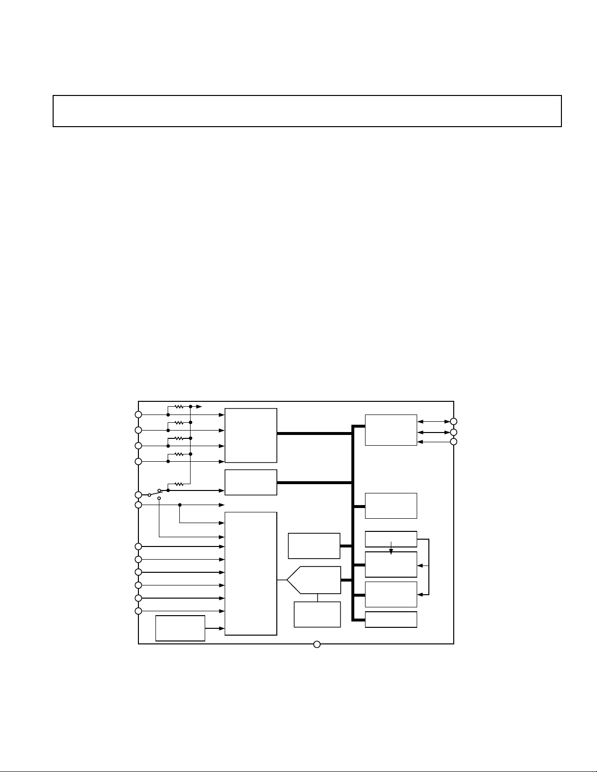
FUNCTIONAL BLOCK DIAGRAM
Hardware Monitor ASIC
ADM1025/ADM1025A*
PRODUCT DESCRIPTION
The ADM1025/ADM1025A is a complete system hardware
monitor for microprocessor-based systems, providing measurement and limit comparison of various system parameters. Five
voltage measurement inputs are provided, for monitoring 2.5 V,
3.3 V, 5 V and 12 V power supplies and the processor core
voltage. The ADM1025/ADM1025A can monitor a sixth power
supply voltage by measuring its own V
dedicated to a remote temperature-sensing diode, and an on-chip
temperature sensor allows ambient temperature to be monitored. The ADM1025A has open-drain VID inputs while the
ADM1025 has on-chip 100 kΩ pull-ups on the VID inputs.
Measured values and in/out of limit status can be read out via
2
an I
C-compatible serial System Management Bus. The device
can be controlled and configured over the same serial bus. The
device also has a programmable INT output to indicate undervoltage, overvoltage and over-temperature conditions.
The ADM1025/ADM1025A’s 3.0 V to 5.5 V supply voltage
range, low supply current, and I
it ideal for a wide range of applications. These include hardware
monitoring and protection applications in personal computers,
electronic test equipment, and office electronics.
. One input (two pins) is
CC
2
C-compatible interface make
V
VID0
VID1
VID2
VID3
300k⍀
/VID4
12V
IN
V
CC
V
CCPIN
2.5V
IN
3.3V
IN
5V
IN
D+
D–/NTI
BANDGAP
TEMPERATURE
SENSOR
*Patent Pending.
I2C is a registered trademark of Philips Corporation.
DD
100k⍀
PULLUPS
VID0–3
REGISTER
VID4
REGISTER
POWER TO CHIP
INPUT
ATTENUATORS
AND
ANALOG
MULTIPLEXER
REV. A
Information furnished by Analog Devices is believed to be accurate and
reliable. However, no responsibility is assumed by Analog Devices for its
use, nor for any infringements of patents or other rights of third parties
which may result from its use. No license is granted by implication or
otherwise under any patent or patent rights of Analog Devices.
SERIAL BUS
INTERFACE
ADD/RST/INT/NTO
SDA
SCL
ADM1025/
ADM1025A
VALUE AND
LIMIT
REGISTERS
ADDRESS
POINTER
REGISTER
ADC
2.5V
BANDGAP
REFERENCE
GND
One Technology Way, P.O. Box 9106, Norwood, MA 02062-9106, U.S.A.
Tel: 781/329-4700 World Wide Web Site: http://www.analog.com
Fax: 781/326-8703 © Analog Devices, Inc., 2000
LIMIT
COMPARATORS
MEASUREMENT
STATUS
REGISTERS
OFFSET
REGISTER
CONFIGURATION
REGISTER

ADM1025/ADM1025A–SPECIFICATIONS
P
arameter Min Typ Max Unit Test Conditions/Comments
(TA = T
MIN
to T
, VCC = V
MAX
MIN
to V
, unless otherwise noted.)
MAX
POWER SUPPLY
Supply Voltage, V
Supply Current, I
CC
CC
3.0 3.30 5.5 V (Note 1)
1.4 2.5 mA Interface Inactive, ADC Active
32 500 µA Standby Mode (Note 2)
TEMPERATURE-TO-DIGITAL CONVERTER
Internal Sensor Accuracy ± 3 °C
Resolution 1 °C
External Diode Sensor Accuracy ± 5 °C
± 3 °C60°C ≤ T
≤ 100°C; VCC = 3.3 V
A
Resolution 1 °C
Remote Sensor Source Current 180 µA High Level
11 µA Low Level
ANALOG-TO-DIGITAL CONVERTER
(INCLUDING MUX AND ATTENUATORS)
Total Unadjusted Error, TUE ±2 % (Note 3)
Differential Nonlinearity, DNL ± 1 LSB
Power Supply Sensitivity ± 1 %/V
Conversion Time (Analog Input or Internal Temperature) 11.6 ms (Note 4)
Conversion Time (External Temperature) 34.8 ms (Note 4)
Input Resistance (2.5 V, 3.3 V, 5 V, 12 V, V
) 100 140 250 kΩ
CCPIN
OPEN-DRAIN DIGITAL OUTPUT ADD/RST/INT/NTO
Output Low Voltage, V
High Level Output Leakage Current, I
OL
OH
0.1 1 µAV
0.4 V I
= –6.0 mA; V
OUT
= VCC; V
OUT
CC
= 3 V
CC
= 3 V
RST Pulsewidth 20 45 ms
OPEN-DRAIN SERIAL DATA BUS OUTPUT (SDA)
Output Low Voltage, V
High Level Output Leakage Current, I
OL
OH
0.1 1 µAV
0.4 V I
= –6.0 mA; VCC = 3 V
OUT
= V
OUT
CC
SERIAL BUS DIGITAL INPUTS (SCL, SDA)
Input High Voltage, V
Input Low Voltage, V
IL
IH
2.1 V
0.8 V
Hysteresis 500 mV
DIGITAL INPUT LOGIC LEVELS
(ADD, VID0–VID4, NTI)
5
VID0–3 Input Resistance 100 kΩ ADM1025 Only
VID4 Input Resistance 300 kΩ ADM1025 Only
100 kΩ ADM1025A
2.1 V
0.8 V
Input High Voltage, V
Input Low Voltage, V
6
IH
6
IL
DIGITAL INPUT LEAKAGE CURRENT
Input High Current, I
Input Low Current, I
IL
Input Capacitance, C
IH
IN
–1 µAV
1 µAV
IN
IN
= V
= 0
CC
5pF
SERIAL BUS TIMING
Clock Frequency, f
Glitch Immunity, t
Bus Free Time, t
Start Setup Time, t
Start Hold Time, t
Stop Condition Setup Time t
SCL Low Time, t
SCL High Time, t
SCL, SDA Rise Time, t
SCL, SDA Fall Time, t
Data Setup Time, t
Data Hold Time, t
NOTES
1
All voltages are measured with respect to GND, unless otherwise specified.
2
Typicals are at TA = 25°C and represent most likely parametric norm. Shutdown current typ is measured with VCC = 3.3 V.
3
TUE (Total Unadjusted Error) includes Offset, Gain and Linearity errors of the ADC, multiplexer and on-chip input attenuators, including an external series input
protection resistor value between zero and 1 kΩ.
4
Total monitoring cycle time is nominally 114.4 ms. Monitoring Cycle consists of 6 Voltage + 1 Internal Temperature + 1 External Temperature readings.
5
ADD is a three-state input that may be pulled high, low or left open-circuit.
6
Timing specifications are tested at logic levels of V
Specifications subject to change without notice.
SCLK
SW
BUF
SU:STA
HD:STA
LOW
HIGH
SU:DAT
HD:DAT
50 ns See Figure 1
1.3 µs See Figure 1
600 ns See Figure 1
600 ns See Figure 1
SU:STO
600 ns See Figure 1
1.3 µs See Figure 1
0.6 µs See Figure 1
R
F
100 ns See Figure 1
300 ns See Figure 1
= 0.8 V for a falling edge and V
IL
= 2.2 V for a rising edge.
IH
400 kHz See Figure 1
300 ns See Figure 1
300 ns See Figure 1
–2–
REV. A

ADM1025/ADM1025A
ABSOLUTE MAXIMUM RATINGS*
Positive Supply Voltage (VCC) . . . . . . . . . . . . . . . . . . . . .6.5 V
Voltage on 12 V V
Pin . . . . . . . . . . . . . . . . . . . . . . . . . 20 V
IN
Voltage on Any Input or Output Pin . . . . . . . . . –0.3 V to +6.5 V
Input Current at Any Pin . . . . . . . . . . . . . . . . . . . . . . . ± 5 mA
Package Input Current . . . . . . . . . . . . . . . . . . . . . . . ± 20 mA
Maximum Junction Temperature (TJ max) . . . . . . . . . . 150°C
Storage Temperature Range . . . . . . . . . . . . –65°C to +150°C
Lead Temperature, Soldering
Vapor Phase 60 sec . . . . . . . . . . . . . . . . . . . . . . . . . . . 215°C
Infrared 15 sec . . . . . . . . . . . . . . . . . . . . . . . . . . . . . . 200°C
ESD Rating All Pins . . . . . . . . . . . . . . . . . . . . . . . . . . 2000 V
ORDERING GUIDE
Temperature Package Package
Model Range Description Option Option
ADM1025ARQ 0°C to 100°C 16-Lead QSOP RQ-16 Integrated 100
ADM1025AARQ 0°C to 100°C 16-Lead QSOP RQ-16 Open-Drain VID Inputs
t
LOW
t
R
t
F
*Stresses above those listed under Absolute Maximum Ratings may cause perma-
nent damage to the device. This is a stress rating only; functional operation of the
device at these or any other conditions above those indicated in the operational
section of this specification is not implied. Exposure to absolute maximum rating
conditions for extended periods may affect device reliability.
THERMAL CHARACTERISTICS
16-Lead QSOP Package:
θ
= 105°C/W
JA
= 39°C/W
θ
JC
kΩ
VID Pull-Ups
t
HD:STA
SCL
SDA
t
t
HD:STA
t
BUF
S
HD:DAT
t
HIGH
t
SU:DAT
t
SU:STA
t
HD:STO
PSP
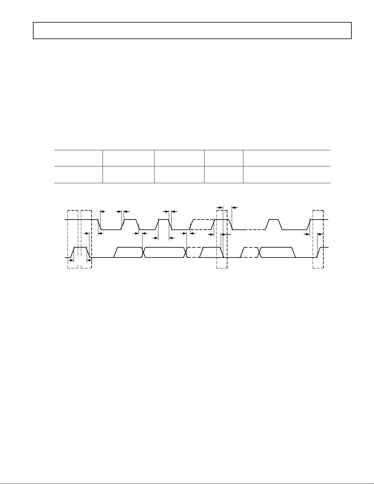
Figure 1. Diagram for Serial Bus Timing
REV. A
–3–

ADM1025/ADM1025A
PIN FUNCTION DESCRIPTIONS
Pin
No. Mnemonic Description
1 SDA Digital I/O. Serial bus bidirectional data. Open-drain output.
2 SCL Digital Input. Serial bus clock.
3 GND System Ground.
4V
CC
5 VID0 Digital Input. Core voltage ID readouts from the processor. This value is read into the VID0–VID3
6 VID1 Digital Input. Core voltage ID readouts from the processor. This value is read into the VID0–VID3
7 VID2 Digital Input. Core voltage ID readouts from the processor. This value is read into the VID0–VID3
8 VID3 Digital Input. Core voltage ID readouts from the processor. This value is read into the VID0–VID3
9 D–/NTI Analog/Digital Input. Connected to cathode of external temperature sensing diode. If held high at
10 D+ Analog Input. Connected to anode of external temperature sensing diode.
11 12 V
12 5 V
13 3.3 V
14 2.5 V
15 V
/VID4 Programmable Analog/Digital Input. Defaults to 12 VIN analog input at power-up, but may be pro-
IN
IN
IN
IN
CCPIN
16 ADD/RST/INT/NTO Programmable Digital I/O. The lowest order programmable bit of the SMBus Address, sampled on
Power. Can be powered by +3.3 V standby power if monitoring in low power states is required.
This pin also serves as the analog input to monitor V
CC
.
Status Register. It has an on-chip 100 kΩ pull-up resistor (ADM1025 only).
Status Register. It has an on-chip 100 kΩ pull-up resistor (ADM1025 only).
Status Register. It has an on-chip 100 kΩ pull-up resistor (ADM1025 only).
Status Register. It has an on-chip 100 kΩ pull-up resistor (ADM1025 only).
power-up, initiates NAND tree test mode.
grammed as VID4 Core Voltage ID readout from the processor. This value is read into the VID4
Status Register. In analog 12 V
mode it has an on-chip voltage attenuator. In VID4 mode it has an
IN
on-chip 300 kΩ pull-up resistor.
Analog Input. Monitors 5 V supply.
Analog Input. Monitors 3.3 V supply.
Analog Input. Monitors 2.5 V supply.
Analog Input. Monitors processor core voltage (0 V to 3.0 V).
SMB activity as a three-state input. Can also be configured to give a minimum 20 ms low reset
output pulse. Alternatively, can be programmed as an interrupt output for temperature/voltage
interrupts. Functions as the output of the NAND tree in NAND tree test mode.
PIN CONFIGURATION
SDA
SCL
GND
V
VID0
VID1
VID2
VID3
1
2
3
4
CC
5
6
7
8
ADM1025/
ADM1025A
TOP VIEW
(Not to Scale)
16
ADD/RST/INT/NTO
V
15
CCPIN
2.5V
14
IN
3.3V
13
IN
5V
12
IN
12V
/VID4
11
IN
10
D+
D–/NTI
9
–4–
REV. A

Typical Performance Characteristics–
ADM1025/ADM1025A
30
20
10
0
–10
–20
–30
TEMPERATURE ERROR – ⴗC
–40
–50
–60
1 1003.3
LEAKAGE RESISTANCE – M⍀
DXP TO GND
DXP TO VCC (5V)
10 30
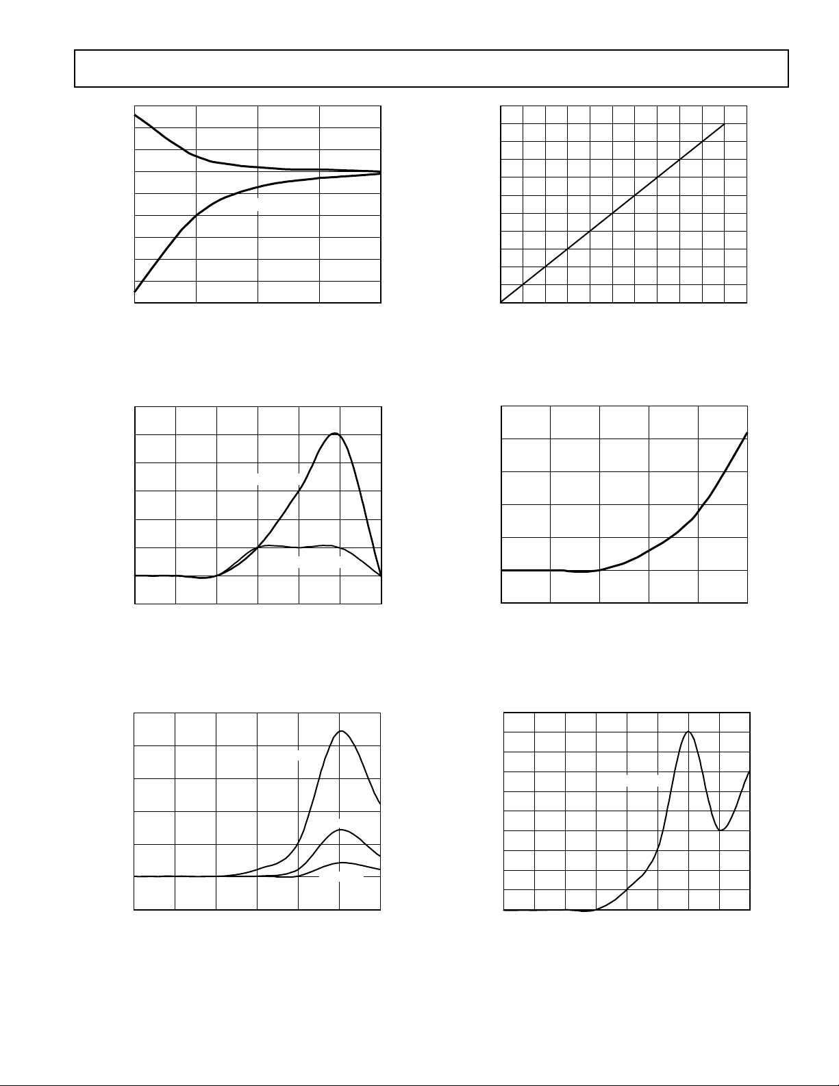
Figure 2. Temperature Error vs. PC Board Track Resistance
6
5
4
250mV p-p REMOTE
3
2
1
TEMPERATURE ERROR – ⴗC
0
100mV p-p REMOTE
120
100
90
80
70
60
50
READING
40
30
20
10
0
0 11010
20 30 40 50
MEASURED TEMPERATURE
60 70 80 90 100
Figure 5. Pentium II® Temperature Measurement vs.
ADM1025/ADM1025A Reading
25
20
15
10
5
TEMPERATURE ERROR – ⴗC
0
–1
50 50M500
5k
50k
FREQUENCY – Hz
500k 5M
Figure 3. Temperature Error vs. Power Supply Noise
Frequency
25
20
15
10
5
TEMPERATURE ERROR – ⴗC
0
–5
50 50M500
5k 50k 500k 5M
FREQUENCY – Hz
100mV p-p
50mV p-p
25mV p-p
Figure 4. Temperature Error vs. Common-Mode Noise
Frequency
–5
1102.2
3.2 4.7 7
DXP-DXN CAPACITANCE – nF
Figure 6. Temperature Error vs. Capacitance Between D+
and D–
10
9
8
TEMPERATURE ERROR – ⴗC
7
6
5
4
3
2
1
0
50 50M500
5k 50k 500k 5M
10mV SQ. WAVE
100k 25M
FREQUENCY – Hz
Figure 7. Temperature Error vs. Differential-Mode Noise
Frequency
Pentium II is a registered trademark of Intel Corporation.
REV. A
–5–
 Loading...