

Low-Cost PC Temperature
a
FEATURES
External Temperature Measurement with Remote
Diode (Two Channels)
On-Chip Temperature Sensor
Interrupt and Over-Temperature Outputs
Fault Tolerant Fan Control
Brownout Detection
LDCM Support
System Management Bus (SMBus)
Standby Mode to Minimize Power Consumption
Limit Comparison of all Monitored Values
APPLICATIONS
Network Servers and Personal Computers
Microprocessor-Based Office Equipment
Test Equipment and Measuring Instruments
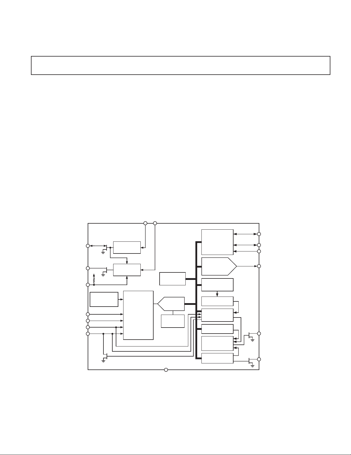
FUNCTIONAL BLOCK DIAGRAM
V
CC
Monitor and Fan Control ASIC
ADM1022
GENERAL DESCRIPTION
The ADM1022 is a low cost temperature monitor and fan controller for microprocessor-based systems. The temperature of one
or two remote sensor diodes may be measured, allowing monitoring of processor temperature in single- or dual-processor systems.
Measured values can be read out via a serial System Management Bus, and values for limit comparisons can be programmed
in over the same serial bus.
The ADM1022 also contains a DAC for fan speed control.
Automatic hardware temperature trip points are provided and
the fan will be driven to full speed if they are exceeded.
Finally, the chip has two supply voltage monitors for brownout
detection.
The ADM1022’s 3.0 V to 5.5 V supply voltage range, low supply
current, and SMBus interface make it ideal for a wide range of
applications. These include hardware monitoring and protection
applications in personal computers, electronic test equipment
and office electronics.
V
MON
RST1
RST2
MR
D1+
D1–
D2+/GPI
D2–/THERM
V
CC
20k⍀
BANDGAP
TEMPERATURE
SENSOR
RESET
GENERATOR 1
RESET
GENERATOR 2
ANALOG
MULTIPLEXER
ADM1022
ADDRESS
POINTER
REGISTER
ADC
2.5V
BANDGAP
REFERENCE
GND
SERIAL BUS
INTERFACE
ANALOG
OUTPUT
REGISTER
AND 8-BIT DAC
VALUE AND
LIMIT
REGISTERS
LIMIT
COMPARATORS
INTERRUPT
STATUS
REGISTERS
INT MASK
REGISTER
MASK
GATING
CONFIGURATION
REGISTER
ADD/NTEST_OUT
SDA
SCL
FAN_SPD/NTEST_IN
INT
FAN_OFF
REV. B
Information furnished by Analog Devices is believed to be accurate and
reliable. However, no responsibility is assumed by Analog Devices for its
use, nor for any infringements of patents or other rights of third parties that
may result from its use. No license is granted by implication or otherwise
under any patent or patent rights of Analog Devices. Trademarks and
registered trademarks are the property of their respective companies.
One Technology Way, P.O. Box 9106, Norwood, MA 02062-9106, U.S.A.
Tel: 781/329-4700 www.analog.com
Fax: 781/326-8703 © 2003 Analog Devices, Inc. All rights reserved.

ADM1022–SPECIFICATIONS
(TA = T
Parameter Min Typ
MIN
to T
, VCC = V
MAX
1
to V
MIN
, unless otherwise noted.)
MAX
Max Unit Test Conditions
POWER SUPPLY
Supply Voltage, V
Supply Current, I
CC
CC
3.0 3.30 5.5 V
1.4 2.6 mA Interface Inactive, ADC Active
TEMPERATURE-TO-DIGITAL CONVERTER
Internal Sensor Accuracy ± 3 ∞C
± 1 ± 2 ∞CT
= 85∞C, Tested at Wafer Sort
A
Resolution 1 ∞C
External Diode Sensor Accuracy ± 5 ∞C
± 3 ∞CT
= 85∞C, Tested at Wafer Sort
A
Resolution 1 ∞C
Remote Sensor Source Current 60 90 130 mAHigh Level (D+ = D– +0.65 V)
3.5 5.5 7.5 mA Low Level (D+ = D– +0.65 V)
Total Monitoring Cycle Time, t
C
200 ms
ANALOG OUTPUT
Output Voltage Range 0 2.5 V
Total Unadjusted Error, TUE ± 5% I
= 2 mA
L
Full-Scale Error ± 1 ± 3%
Zero Error ± 2 LSB No Load
Differential Nonlinearity, DNL ± 1 LSB Monotonic by Design
Integral Nonlinearity ± 1 LSB
Output Source Current 2 mA
Output Sink Current 1 mA
VOLTAGE MONITOR THRESHOLDS
Reset Threshold, V
MON
, V
CC
2.85 2.925 3.00 V Measured with VCC Falling
Hysteresis 50 mV
MR INPUT
MR Minimum Pulsewidth, t
MR
10 ms
MR Glitch Immunity 100 ns
MR to RST2 Propagation Delay, t
MD
0.5 ms
MR Pull-Up Resistance 10 20 30 kW
RESET OUTPUTS, RST1, RST2
Reset Output Voltage, V
Reset Active Timeout Period, t
VCC to Reset Delay, t
DIGITAL OUTPUT ADD/NTEST_OUT
Output High Voltage, V
Output Low Voltage, V
OL
RP
D
2
OH
OL
140 180 560 ms
20 ms
2.4 V I
0.3 V I
0.4 V
= 1.2 mA
SINK
V
= VTH(MAX)
CC
= 3.0 mA
OUT
OPEN-DRAIN DIGITAL OUTPUTS
(INT, THERM, RST2, RST1)
Output Low Voltage, V
High Level Output Leakage Current, I
OL
OH
0.1 1 mAV
0.4 V I
= –3.0 mA
OUT
= V
OUT
CC
OPEN-DRAIN SERIAL DATA
BUS OUTPUT (SDA)
Output Low Voltage, V
High Level Output Leakage Current, I
OL
OH
0.4 V I
0.1 1 mAV
= –3.0 mA
OUT
= V
OUT
CC
SERIAL BUS DIGITAL INPUTS
(SCL, SDA)
Input High Voltage, V
Input Low Voltage, V
IL
IH
2.1 V (min)
0.8 V (max)
Input Leakage Current ±5 mA
Hysteresis 500 mV
–2–
REV. B
Parameter Min Typ Max Unit Test Conditions
DIGITAL INPUT LOGIC LEVELS
(FAN_SPD/NTEST_IN,
ADD/NTEST_OUT, MR, GPI)
Input High Voltage, V
Input Low Voltage, V
IL
IH
2.2 V
0.8 V
DIGITAL INPUT LEAKAGE CURRENT
(ALL DIGITAL INPUTS)
Input High Current, I
Input Low Current, I
Input Capacitance, C
SERIAL BUS TIMING
Clock Frequency, f
Glitch Immunity, t
Bus Free Time, t
Start Setup Time, t
Start Hold Time, t
Stop Condition Setup Time, t
SCL Low Time, t
SCL High Time, t
SCL, SDA Rise Time, t
SCL, SDA Fall Time, t
Data Setup Time, t
Data Hold Time, t
NOTES
1
Typicals are at TA = 25∞C and represent most likely parametric norm. Standby current typ is measured with VCC = 3.3 V.
2
ADD is a three-state input that may be pulled high, low or left open-circuit.
3
Timing specifications are tested at logic levels of V
Specifications subject to change without notice.
SCLK
SW
BUF
SU:STA
HD:STA
LOW
HIGH
SU:DAT
HD:DAT
IH
IL
IN
3
SU:STO
R
F
= 0.8 V for a falling edge and V
IL
–1 –0.005 mAV
+0.005 +1 mAV
5pF
400 kHz See Figure 1
50 ns See Figure 1
1.3 ms See Figure 1
600 ns See Figure 1
600 ns See Figure 1
600 ns See Figure 1
1.3 ms See Figure 1
0.6 ms See Figure 1
300 ns See Figure 1
300 ns See Figure 1
100 ns See Figure 1
300 ns See Figure 1
= 2.2 V for a rising edge.
IH
IN
IN
= V
= 0
CC
ADM1022
SCLK
SDATA
t
BUF
PS
t
HD;STA
t
LOW
t
R
t
HD;DAT
t
HIGH
t
F
t
SU;DAT
Figure 1. Diagram for Serial Bus Timing
t
HD;STA
t
SU;STA
S
t
SU;STO
P
REV. B
–3–

ADM1022
ABSOLUTE MAXIMUM RATINGS*
Positive Supply Voltage (VCC) . . . . . . . . . . . . . . . . . . . . 6.5 V
Voltage On Digital Inputs Except Therm . . –0.3 V to +6.5 V
Voltage On Therm Pin . . . . . . . . . . . . –0.3 V to V
+ 0.3 V
CC
Voltage on Any Other Input
or Output Pin . . . . . . . . . . . . . . . . . . –0.3 V to V
+ 0.3 V
CC
Input Current at Any Pin . . . . . . . . . . . . . . . . . . . . . . . ± 5 mA
Package Input Current . . . . . . . . . . . . . . . . . . . . . . . ± 20 mA
Maximum Junction Temperature (T
max) . . . . . . . . . . 150∞C
J
Storage Temperature Range . . . . . . . . . . . . –65∞C to +150∞C
Lead Temperature, Soldering
Vapor Phase 60 sec . . . . . . . . . . . . . . . . . . . . . . . . . . 215∞C
Infrared 15 sec . . . . . . . . . . . . . . . . . . . . . . . . . . . . . 200∞C
ESD Rating (Human Body Model) . . . . . . . . . . . . . . . 4000 V
PIN CONFIGURATION
MR
RST1
GND
V
V
MON
RST2
1
2
3
4
5
CC
6
7
8
FAN_OFF
FAN_SPD/NTEST_IN
*Stresses above those listed under Absolute Maximum Ratings may cause perma-
nent damage to the device. This is a stress rating only; functional operation of the
device at these or any other conditions above those indicated in the operational
section of this specification is not implied. Exposure to absolute maximum rating
conditions for extended periods may affect device reliability.
THERMAL CHARACTERISTICS
16-Lead QSOP Package
q
= 105∞C/W
JA
= 39∞C/W
q
JA
ORDERING GUIDE
Temperature Package Package
Model Range Description Option
ADM1022ARQ 0∞C to 85∞C 16-Lead QSOP RQ-16
16
SDA
15
SCL
14
INT
ADM1022
TOP VIEW
(Not to Scale)
13
ADD/NTEST_OUT
12
D2+/GPI
11
D2–/THERM
10
D1+
9
D1–
CAUTION
ESD (electrostatic discharge) sensitive device. Electrostatic charges as high as 4000 V readily
accumulate on the human body and test equipment and can discharge without detection.
Although the ADM1022 features proprietary ESD protection circuitry, permanent damage may
occur on devices subjected to high energy electrostatic discharges. Therefore, proper ESD
precautions are recommended to avoid performance degradation or loss of functionality.
–4–
REV. B

ADM1022
PIN FUNCTION DESCRIPTIONS
Pin
No. Mnemonic Description
1 FAN_OFF Digital Output (Open-Drain) Fan Off Request. When asserted low this indicates a request to shut
off the fan independent of the FAN_SPD output. When negated (output FET off) it indicates that
the fan may be turned on.
2 MR Digital Input, Manual Reset. A logic low on this input causes RST2 to be asserted. Once this input
is negated that output will remain asserted for t
Leave unconnected if not used.
3 RST1 Digital I/O (Open-Drain). This pin is asserted low while V
remains asserted for t
after the reset condition is terminated. It is bidirectional so the ADM1022 can
RP
be optionally reset; external logic must be used to prevent system auxiliary reset from occurring
when used as an input.
4 GND GROUND. Power and Signal Ground.
5V
6V
CC
MON
POWER 3.3 V. Power source and voltage monitor input for first reset generator.
Analog Input. Voltage monitor input for second reset generator.
7 RST2 Digital Output (Open-Drain). This pin is asserted low under any of the following conditions:
– V
or VCC remains below the reset threshold
MON
– while MR is held low
– while RST1 is asserted.
It remains asserted for t
after the reset conditions are terminated.
RP
8 FAN_SPD/NTEST_IN Analog Output/Test Input. An active-high input that enables NAND board-level connectivity testing.
Refer to section on NAND testing. Used as an analog output for fan speed control when NAND
test is not selected.
9 D1– Remote Thermal Diode Negative Input. This is the negative input (current sink) from the remote
thermal diode. This also serves as the negative input into the A/D.
10 D1+ Remote Thermal Diode Positive Input. This is the positive input (current source) from the remote
thermal diode. This serves as the positive input into the A/D.
11 D2–/THERM Analog Input/Digital I/O (Open-Drain). Can be programmed as negative input for a second diode
temperature sensor, or as a digital I/O pin. In this case it is an active low thermal overload output
that indicates a violation of a temperature set point (over-temperature). Also acts as an input to
provide external fan control. When this pin is pulled low by an external signal, a status bit is set and
the fan speed is set to full on.
12 D2+/GPI Analog/Digital Input. Can be programmed as the positive input for a second diode sensor, or as a
general-purpose logic input. In this case it can be programmed as an active high or active low input
that sets Bit 4 of the Status Registers. This bit can only be reset by reading the status registers, pro-
vided GPI is in the inactive state.
13 ADD/NTEST_OUT Digital I/O. The lowest order programmable bit of the SMBus Address. ADD is sampled at power-
up and changing it while powered on will have no immediate effect. This pin also functions as an
output when doing a NAND test.
14 INT Digital Output (Open Drain), System Interrupt Output. This signal indicates a violation of a set
trip point. The output is enabled when Bit 1 of the Configuration Register is set to 1. The default
state is disabled.
15 SCL Digital Input SMBus Clock.
16 SDA Digital I/O (Open-Drain) SMBus Bidirectional Data.
. This input has an internal 20 kW pull-up resistor.
RP
remains below the reset threshold. It
CC
REV. B
–5–
ADM1022
–Typical Performance Characteristics
30
20
10
0
–10
–20
–30
TEMPERATURE ERROR – ⴗC
–40
–50
–60
1 1003.3
LEAKAGE RESISTANCE – M⍀
DXP TO GND
DXP TO VCC (5V)
10 30
TPC 1. Temperature Error vs. PC Leakage Resistance
6
5
4
250mV p-p REMOTE
3
2
120
100
90
80
70
60
50
READING
40
30
20
10
0
0 11010
20 30 40 50
MEASURED TEMPERATURE
60 70 80 90 100
TPC 4. Pentium® III Temperature Measurement vs.
ADM1022 Reading
30
25
20
15
10
ERROR
1
TEMPERATURE ERROR – ⴗC
0
–1
50 50M500
5k
50k
FREQUENCY – Hz
100mV p-p REMOTE
500k 5M
TPC 2. Temperature Error vs. Power Supply Noise
Frequency
25
20
15
10
5
TEMPERATURE ERROR – ⴗC
0
–5
50 50M500
5k 50k 500k 5M
FREQUENCY – Hz
100mV p-p
50mV p-p
25mV p-p
5
TEMPERATURE ERROR – ⴗC
0
–5
1.0 29.02.2
3.2 4.7 7.0
DXP-DXN CAPACITANCE – nF
10.0 14.0 22.0
TPC 5. Temperature Error vs. Capacitance Between D+
and D–
80
70
60
50
40
30
SUPPLY CURRENT – A
20
10
0
0
5k 10k 25k 50k 75k 100k 250k 500k 750k
SCLK FREQUENCY – Hz
VCC = 5V
VCC = 3V
1M1k
TPC 3. Temperature Error vs. Common-Mode Noise
Frequency
Pentium is a registered trademark of Intel Corporation.
–6–
TPC 6. Standby Current vs. Clock Frequency
REV. B

ADM1022
10
9
8
TEMPERATURE ERROR – ⴗC
7
6
5
4
3
2
1
0
50 50M500
5k 50k 500k 5M
10mV SQ. WAVE
100k 25M
FREQUENCY – Hz
TPC 7. Temperature Error vs. Differential-Mode Noise
Frequency
2.3
2.2
2.1
2.0
1.9
SUPPLY CURRENT – mA
1.8
VDD = 3.0V
1.7
VDD = 5.5V
VDD = 3.3V
TEMPERATURE – ⴗC
1109070503010–10–30
130
TPC 8. Standby Supply Current vs. Supply Voltage
400
GENERAL DESCRIPTION
The ADM1022 is a low-cost temperature monitor and fan controller for microprocessor-based systems. The temperature of
one or two remote sensor diodes may be measured, allowing
monitoring of processor temperature in single- or dual-processor
systems. The chip also contains an on-chip sensor to allow
ambient temperature to be monitored.
Measured values can be read out via a serial System Management Bus, and values for limit comparisons can be programmed
in over the same serial bus.
The ADM1022 also contains a DAC for fan speed control.
Automatic hardware temperature trip points are provided for
fault tolerant fan control and the fan will be driven to full speed
if they are exceeded. Two interrupt outputs are provided, which
will be asserted if the software or hardware limits are exceeded.
Finally, the chip has two supply voltage monitors for brownout
detection. These drive two reset pins, one of which is bidirectional. A manual reset input is also provided.
INTERNAL REGISTERS OF THE ADM1022
A brief description of the ADM1022’s principal internal registers is given below. More detailed information on the function
of each register is given in Tables IV to IX.
Configuration Register: Provides control and configuration.
Address Pointer Register: This register contains the address that
selects one of the other internal registers. When writing to the
ADM1022, the first byte of data is always a register address, which
is written to the Address Pointer Register.
Interrupt (INT) Status Register: This register provides status
of each Interrupt event. It is also mirrored by a second register
at address 4Ch.
Interrupt (INT) Mask Register: Allows masking of individual
interrupt sources.
Value and Limit Registers: The results of temperature measurements are stored in these registers, along with their limit values.
Analog Output Register: The code controlling the analog output DAC is stored in this register.
350
300
250
200
POWER RESET TIMEOUT – ms
150
100
TPC 9. Power-up Reset vs. Temperature
REV. B
RST2
RST1
TEMPERATURE – ⴗC
SERIAL BUS INTERFACE
Control of the ADM1022 is carried out via the serial bus. The
ADM1022 is connected to this bus as a slave device, under the
control of a master device, e.g., the PIIX4.
The ADM1022 has a 7-bit serial bus address. When the device is
powered up, it will do so with a default serial bus address. The five
MSBs of the address are set to 01011, the two LSBs are determined by the logical states of Pin 13 (ADD/NTEST_OUT).
This is a three-state input that can be grounded, connected to V
CC
or left open-circuit to give three different addresses. The state of
the ADD pin is only sampled at power-up, so changing ADD
1301109070503010–10–30
with power-on will have no effect until the device is powered
off then on again.
–7–

ADM1022
Table I. ADD Pin Truth Table
ADD Pin A1 A0
GND 1 0
No Connect 0 0
V
CC
If ADD is left open-circuit the default address will be 0101100.
The facility to make hardwired changes to A1 and A0 allows the
user to avoid conflicts with other devices sharing the same serial
bus; for example, if more than one ADM1022 is used in a system.
The serial bus protocol operates as follows:
1. The master initiates data transfer by establishing a START
condition, defined as a high-to-low transition on the serial
data line SDA while the serial clock line SCL remains high.
This indicates that an address/data stream will follow. All
slave peripherals connected to the serial bus respond to the
START condition, and shift in the next eight bits, consisting
of a 7-bit address (MSB first) plus an R/W bit, which determines the direction of the data transfer, i.e., whether data
will be written to or read from the slave device.
The peripheral whose address corresponds to the transmitted
address responds by pulling the data line low during the low
period before the ninth clock pulse, known as the Acknowledge Bit. All other devices on the bus now remain idle while
the selected device waits for data to be read from or written
to it. If the R/W bit is a 0, the master will write to the slave
device. If the R/W bit is a one, the master will read from the
slave device.
2. Data is sent over the serial bus in sequences of nine clock
pulses, eight bits of data followed by an Acknowledge Bit
from the slave device. Transitions on the data line must
occur during the low period of the clock signal and remain
stable during the high period, as a low-to-high transition when
the clock is high may be interpreted as a STOP signal. The
number of data bytes that can be transmitted over the serial
bus in a single READ or WRITE operation is limited only by
what the master and slave devices can handle.
3. When all data bytes have been read or written, stop conditions
are established. In WRITE mode, the master will pull the
data line high during the 10th clock pulse to assert a STOP
condition. In READ mode, the master device will override
the acknowledge bit by pulling the data line high during the
low period before the 9th clock pulse. This is known as No
Acknowledge. The master will then take the data line low
during the low period before the 10th clock pulse, then high
during the 10th clock pulse to assert a STOP condition.
Any number of bytes of data may be transferred over the serial
bus in one operation, but it is not possible to mix read and write
in one operation, because the type of operation is determined at
the beginning and cannot subsequently be changed without
starting a new operation.
01
In the case of the ADM1022, write operations contain either
one or two bytes, and read operations contain one byte, and
perform the following functions:
To write data to one of the device data registers or read data
from it, the Address Pointer Register must be set so that the
correct data register is addressed, then data can be written into
that register or read from it. The first byte of a write operation
always contains an address that is stored in the Address Pointer
Register. If data is to be written to the device, then the write
operation contains a second data byte that is written to the register selected by the address pointer register.
This is illustrated in Figure 2a. The device address is sent over
the bus followed by R/W set to 0. This is followed by two data
bytes. The first data byte is the address of the internal data
register to be written to, which is stored in the Address Pointer
Register. The second data byte is the data to be written to the
internal data register.
When reading data from a register there are two possibilities:
1. If the ADM1022’s Address Pointer Register value is unknown
or not the desired value, it is first necessary to set it to the correct value before data can be read from the desired data register.
This is done by performing a write to the ADM1022 as before,
but only the data byte containing the register address is sent,
as data is not to be written to the register. This is shown in
Figure 2b.
A read operation is then performed consisting of the serial bus
address, R/W bit set to 1, followed by the data byte read from
the data register. This is shown in Figure 2c.
2. If the Address Pointer Register is known to be already at the
desired address, data can be read from the corresponding
data register without first writing to the Address Pointer Register, so Figure 2b can be omitted.
NOTES
1. Although it is possible to read a data byte from a data register
without first writing to the Address Pointer Register, if the
Address Pointer Register is already at the correct value, it is
not possible to write data to a register without writing to the
Address Pointer Register, because the first data byte of a
write is always written to the Address Pointer Register.
2. In Figures 2a to 2c, the serial bus address is shown as the
default value 01011(A1)(A0), where A1 and A0 are set by
the three-state ADD pin.
3. The ADM1022 also supports the Read Byte protocol, as
described in the System Management Bus specification.
–8–
REV. B

ADM1022
D0
9
9
ACK. BY
ADM1022
STOP BY
MASTER
SCL
SDA
START BY
MASTER
19
0
1011
FRAME 1
SERIAL BUS ADDRESS
BYTE
(CONTINUED)
SDA (CONTINUED)
A0
A1
SCL
W
R/
ADM1022
ACK. BY
D7
1
D6
D7
ADDRESS POINTER REGISTER BYTE
1
D5
D6
D5
D4
FRAME 3
DATA BYTE
D4
FRAME 2
D3
D3
D2
D2
D1
D1
D0
ACK. BY
ADM1022
Figure 2a. Writing a Register Address to the Address Pointer Register, then Writing Data to the Selected Register
D0
9
ACK. BY
ADM1022
STOP BY
MASTER
SCL
SDA
START BY
MASTER
19
0
1011
FRAME 1
SERIAL BUS ADDRESS
BYTE
A0
A1
R/W
ADM1022
ACK. BY
1
D6
D7
ADDRESS POINTER REGISTER BYTE
D5
D4
FRAME 2
D3
D2
D1
Figure 2b. Writing to the Address Pointer Register Only
19
SCL
0
SDA
START BY
MASTER
1011
FRAME 1
SERIAL BUS ADDRESS
BYTE
A0
A1
R/W
ACK. BY
ADM1022
Figure 2c. Reading Data from a Previously Selected Register
TEMPERATURE MEASUREMENT SYSTEM
Internal Temperature Measurement
The ADM1022 contains an on-chip bandgap temperature
sensor. The on-chip ADC performs conversions on the output of this sensor and outputs the temperature data in 8-bit
twos complement format. The format of the temperature data
is shown in Table II.
External Temperature Measurement
The ADM1022 can measure the temperature of two external
diode sensors or diode-connected transistors, connected to Pins
9 and 10 or 11 and 12.
Pins 9 and 10 are a dedicated temperature input channel. The
default function of Pins 11 and 12 is the THERM input/output
and a general purpose logic input (GPI), but they can be configured to measure a diode sensor by setting Bit 7 of the Configuration Register to 1.
D0
NO ACK.
BY MASTER
9
STOP BY
MASTER
1
D6
D7
D4
D5
FRAME 2
DATA BYTE FROM ADM1022
D3
D2
D1
The forward voltage of a diode or diode-connected transistor,
operated at a constant current, exhibits a negative temperature
coefficient of about –2 mV/∞C. Unfortunately, the absolute value
, varies from device to device, and individual calibra-
of V
BE
tion is required to null this out, so the technique is unsuitable
for mass-production.
The technique used in the ADM1022 is to measure the change
in V
when the device is operated at two different currents.
BE
This is given by:
DV
= KT/q ¥ ln(N)
BE
where:
K is Boltzmann’s constant
q is charge on the carrier
T is absolute temperature in Kelvins
N is ratio of the two currents
REV. B
–9–

ADM1022
Figure 3 shows the input signal conditioning used to measure
the output of an external temperature sensor. This figure
shows the external sensor as a substrate transistor, provided
for temperature monitoring on some microprocessors, but it
could equally well be a discrete transistor.
V
DD
I
N ⴛ II
BIAS
V
V
OUT+
OUT–
TO
ADC
REMOTE
SENSING
TRANSISTOR
D+
D–
BIAS
DIODE
LOW-PASS
FILTER
= 65kHz
f
C
Figure 3. Signal Conditioning
If a discrete transistor is used, the collector will not be grounded,
and should be linked to the base. If a PNP transistor is used the
base is connected to the D– input and the emitter to the D+ input.
If an NPN transistor is used, the emitter is connected to the D–
input and the base to the D+ input.
Table II. Temperature Data Format
LAYOUT CONSIDERATIONS
Digital boards can be electrically noisy environments, and care
must be taken to protect the analog inputs from noise, particularly when measuring the very small voltages from a remote
diode sensor. The following precautions should be taken:
1. Place the ADM1022 as close as possible to the remote sensing diode. Provided that the worst noise sources such as
clock generators, data/address buses and CRTs are avoided,
this distance can be four to eight inches.
2. Route the D+ and D– tracks close together, in parallel, with
grounded guard tracks on each side. Provide a ground plane
under the tracks if possible.
3. Use wide tracks to minimize inductance and reduce noise
pickup. 10 mil track minimum width and spacing is
recommended.
GND
D+
D–
GND
10MIL
10MIL
10MIL
10MIL
10MIL
10MIL
10MIL
Temperature Digital Output
–128∞C 1000 0000
–125∞C 1000 0011
–100∞C 1001 1100
–75∞C 1011 0101
–50∞C 1100 1110
–25∞C 1110 0111
–1∞C 1111 1111
0∞C 0000 0000
+1∞C 0000 0001
+10∞C 0000 1010
+25∞C 0001 1001
+50∞C 0011 0010
+75∞C 0100 1011
+100∞C 0110 0100
+125∞C 0111 1101
+127∞C 0111 1111
To prevent ground noise interfering with the measurement, the
more negative terminal of the sensor is not referenced to ground,
but is biased above ground by an internal diode at the D– input.
If the sensor is used in a very noisy environment, a capacitor of
value up to 1000 pF may be placed between the D+ and D–
inputs to filter the noise.
To measure DV
, the sensor is switched between operating
BE
currents of I and N ¥ I. The resulting waveform is passed through
a 65 kHz low-pass filter to remove noise, thence to a chopperstabilized amplifier that performs the functions of amplification
and rectification of the waveform to produce a dc voltage proportional to DV
. This voltage is measured by the ADC to give
BE
a temperature output in 8-bit twos complement format. To
further reduce the effects of noise, digital filtering is performed
by averaging the results of 16 measurement cycles. An external
temperature measurement takes nominally 9.6 ms.
Figure 4. Arrangement of Signal Tracks
4. Try to minimize the number of copper/solder joints, which
can cause thermocouple effects. Where copper/solder joints
are used, make sure that they are in both the D+ and D–
path and at the same temperature.
Thermocouple effects should not be a major problem as 1∞C
corresponds to about 200 mV, and thermocouple voltages are
about 3 mV/
o
C of temperature difference. Unless there are
two thermocouples with a big temperature differential between
them, thermocouple voltages should be much less than 200 mV.
5. Place 0.1 mF bypass and 1000 pF input filter capacitors close
to the ADM1022.
6. If the distance to the remote sensor is more than eight inches,
the use of twisted pair cable is recommended. This will work
up to about 6 to 12 feet.
7. For really long distances (up to 100 feet) use a shielded
twisted pair such as Belden #8451 microphone cable. Connect the twisted pair to D+ and D– and the shield to GND
close to the ADM1022. Leave the remote end of the shield
unconnected to avoid ground loops.
Because the measurement technique uses switched current
sources, excessive cable and/or filter capacitance can affect the
measurement. When using long cables, the filter capacitor C1
may be reduced or removed. In any case, the total shunt capacitance should not exceed 1000 pF.
Cable resistance can also introduce errors. 1 W series resistance
introduces about 0.5∞C error.
–10–
REV. B

ADM1022
ANALOG OUTPUT
The ADM1022 has a single analog output (FAN_SPD) from an
unsigned 8-bit DAC that produces 0 V–2.5 V. The analog output register defaults to 00 during power-on reset, which produces
minimum fan speed. The analog output may be amplified and
buffered with external circuitry such as an op amp and transistor
to provide fan speed control.
Suitable fan drive circuits are given in Figures 5a to 5e. When
using any of these circuits, the following points should be noted:
1. All of these circuits will provide an output range from zero to
almost +V
2. To amplify the 2.5 V range of the analog output up to +V
FAN
.
,
FAN
the gain of these circuits needs to be set as shown.
3. Care must be taken when choosing the op amp to ensure that
its input common-mode range and output voltage swing are
suitable.
4. The op amp may be powered from the +V rail alone. If it
is powered from +V then the input common-mode range
should include ground to accommodate the minimum output
voltage of the DAC, and the output voltage should swing below
0.6 V to ensure that the transistor can be turned fully off.
5. In all these circuits, the output transistor must have an I
CMAX
greater than the maximum fan current, and be capable of dissipating power due to the voltage dropped across it when the
fan is not operating at full speed.
6. If the fan motor produces a large back ElectroMotive Force
(EMF) when switched off, it may be necessary to add clamp
diodes to protect the output transistors in the event that the
output goes from full-scale to zero very quickly.
7. Pulling FAN_SPD/NTEST_IN high externally on power-up
causes NAND Test Mode to be invoked on the ADM1022.
Therefore, a 4.7 kW pull-down resistor should be added
externally to the FAN_SPD pin to prevent ADM1022 inadvertently entering the NAND Tree Test Mode.
Figure 5c shows how the FAN_OFF signal may be used (with
any of the control circuits) to gate the fan on and off independent of the value on the FAN_SPD/NTEST_IN pin.
5V
FAN_SPD
AD8541
+
Q1
NDT452 P
12V
R4
R3
1k⍀
1k⍀
Q1
BD136
2SA968
FAN_SPD
R1
10k⍀
AD8519
+
39k⍀
R2
Figure 5b. 12 V Fan Circuit with Op Amp and PNP
Transistor
12V
R2
39k⍀
100k⍀
R4
1k⍀
R3
Q1
NDT452 P
3.3V
Q2
NDT3055L
FAN_SPD
R1
10k⍀
AD8519
+
FAN_OFF
Figure 5c. 12 V Fan Circuit with Op Amp and P-Channel
MOSFET
12V
FAN_SPD
5k⍀
R3
100k⍀
MBT3904
R5
Q1/Q2
DUAL
R4
100k⍀
3.9k⍀
R2
R1
1k⍀
Q3
NDT452 P
Figure 5d. Discrete 12 V Fan Drive Circuit with
P-Channel MOSFET, Single Supply
12V
REV. B
R2
R1
10k⍀
15k⍀
5V
FAN
Figure 5a. 5 V Fan Circuit with Op Amp
FAN_SPD
5k⍀
R5
100k⍀
MBT3904
R6
Q1/Q2
DUAL
R4
100k⍀
R3
100⍀
Q3
BC556
2N3906
R2
3.9k⍀
R1
1k⍀
Figure 5e. Discrete 12 V Fan Drive Circuit with Bipolar
Output Single Supply
–11–
Q4
BD132
TIP32A

ADM1022
FAULT TOLERANT FAN CONTROL
The ADM1022 incorporates a fault tolerant fan control capability that is tied to operation of the THERM output. It can override the setting of the analog output and force it to maximum to
give full fan speed in the event of a critical over-temperature
problem, even if, for some reason, this has not been handled by
the system software.
There are four temperature set point registers that will activate
the fault tolerant fan control. Two of these limits are programmable by the user and two are hardware (read-only) registers
that will operate if the user does not program any limits. The
fault tolerant fan control is activated if a limit is exceeded for
three or more consecutive readings. These limits are separate
from the normal high and low temperature limits for the INT
output, which do not affect the fault tolerant fan control or
THERM output.
A hardware limit of 70∞C for the on-chip temperature sensor is
programmed into the register at address 13h. For the remote
sensors, a hardware limit of 100∞C is programmed in to the
register at address 17h. These are the default limits and the analog output will be forced to full-scale if the on-chip sensor reads
more than 70∞C or either of the remote sensors reads more than
100∞C. This makes the fault tolerant fan control fail-safe in that it
will operate at these temperatures even if the user has programmed
no other limits, or in the event of a software malfunction.
The user may override these default limits by programming new
limits into registers at address 14h for the on-chip sensor and
18h for the remote sensors. The default values in these registers
are the same as for the read-only registers (70∞C and 100∞C),
but they may be programmed with higher or lower values.
Once registers 13h and 14h have been programmed, or if the
default is acceptable, Bit 1 of the configuration register must be
set to “1.” This bit is a write-once bit that can only be written to
“1” and it has two effects:
1. It makes the values in registers 13h and 14h the active limits,
and disables read-only registers 17h and 18h.
2. It locks the data into registers 13h and 14h, so they cannot
be changed until the lock bit is reset, which is when RST2 is
asserted or a Power-On Reset occurs.
Once the hardware override of the analog output is triggered, it will
only return to normal operation after three consecutive measurements that are five degrees lower than each of the above limits.
The analog output can also be forced to full-scale by pulling the
THERM pin (Pin 11) low. Bit 6 of the Status Register is also set.
Whenever FAN_SPD output is forced to full-scale, the FAN_OFF
output is negated.
THE ADM1022 INTERRUPT SYSTEM
The ADM1022 has two interrupt outputs, INT and THERM.
These have different functions. INT responds to violations of
software programmed temperature limits and its interrupt sources
are maskable, as described in more detail later. THERM is
intended as a “fail-safe” interrupt output that cannot be masked.
Interrupts and status bits are only set if a limit is exceeded for at
least three consecutive conversions.
Operation of the INT output is illustrated in Figure 6. Assuming that the temperature starts off within the programmed limits
and that temperature interrupt sources are not masked, INT
will go low if the temperature measured by any of the internal or
external sensors goes outside the programmed high or low
temperature limit for that sensor. INT also goes low whenever
THERM is low.
100ⴗC
90ⴗC
80ⴗC
70ⴗC
60ⴗC
50ⴗC
40ⴗC
INT
ACPI CONTROL
CLEAR EVENT
*
TEMP
*
METHODS
*ACPI AND DEFAULT CONTROL METHODS
ADJUST TEMPERATURE LIMIT VALUES
Figure 6. Operation of
*
HIGH LIMIT
*
*
LOW LIMIT
*
INT
Output
Once the interrupt has been cleared, it will not be reasserted
even if the temperature remains outside the limit previously
exceeded. However, INT will be reasserted if:
a) the temperature goes outside the other limit for the sensor
or
b) the previously exceeded limit is reprogrammed and the tem-
perature is then outside the new limit on the next conversion
cycle
or
c) an interrupt is generated by another source.
INTERRUPT MASKING
Any of the bits in the Interrupt Status Register can be masked out
by setting the corresponding mask bit in the Interrupt Mask Register. That interrupt source will then no longer generate an interrupt.
However, the bits in the status register will be set as normal.
INTERRUPT CLEARING
Reading the Interrupt Status Register will output the contents of
the Register, then clear it. It will remain cleared until the monitoring cycle updates it, so the next read operation should not be
performed on the register until this has happened, or the result
will be invalid.
The INT output is cleared with the INT_Clear bit, which is Bit
2 of the Configuration Register, without affecting the contents
of the Interrupt (INT) Status Registers.
INTERRUPT STATUS MIRROR REGISTER
Whenever a bit in the Interrupt Status Register is set, the corresponding bit is also set in the mirror register at address 4Ch.
This register allows a second management system to access the
status data without worrying about clearing the data. The data
in this register is for reading only and has no effect on the interrupt output. The contents of this register are cleared when read.
–12–
REV. B

ADM1022
THERM INPUT/OUTPUT
Pin 11 may be configured as an input for a second temperature
sensor by setting Bit 7 of the Configuration Register, or it may
be used as an interrupt output by clearing Bit 7 of the Configuration Register, which is its default condition. The Thermal
Management Input/Output (THERM) is a logic input/opendrain output. It can also function as a logic input. If THERM is
taken low by an external source, the analog output will be forced
to FFh to switch a controlled fan to maximum speed and
FAN_OFF will be negated.
THERM OPERATING MODE
THERM responds only to the “hardware” temperature limits
at addresses 13h, 14h, 17h and 18h, not to the software programmed limits. The function of these registers was described
earlier with regard to fault tolerant fan speed control.
HARDWARE
TRIP POINT
5ⴗ
TEMP
THERM
ANALOG
OUTPUT
FROM
VALUE
AND LIMIT
REGISTERS
PROGRAMMED
VALUE
FF
H
Figure 7. Operation of
HIGH
LIMIT
VALUE
LOW
LIMIT
COMPARA-
HIGH
AND
LOW
LIMIT
TORS
1 = OUT
OF
LIMIT
THERM
GPI
DATA
DEMULTI-
PLEXER
Output
EXT
FF
H
THERM
INPUT
INT. TEMP
EXT. TEMP2
DIODE 2 FAULT
RESERVED
GPI
EXT. TEMP1
THERM
DIODE 1 FAULT
MASKING
DATA
FROM BUS
8 MASK BITS
(SAME BIT
ORDER AS
STATUS
REGISTER)
0
1
2
INTERRUPT
3
STATUS
4
REGISTER
5
6
7
INTERRUPT
MASK
REGISTER
THERM will go low if the hardware temperature limit is exceeded
for three consecutive measurements. It will remain low until the
temperature falls five degrees below the limit for three consecutive measurements. While THERM is low, the analog output
will go to FFh to boost a controlled fan to full speed and
FAN_OFF will be negated.
When the Fault Tolerant Fan Control state is exited, the analog
FAN_SPD output returns to its previously programmed value,
which may have been changed during the time that the FAN_SPD
output was forced to FFh.
INTERRUPT STRUCTURE
The Interrupt Structure of the ADM1022 is shown in more
detail in Figure 8. As each measurement value is obtained and
stored in the appropriate value register, the value and the limits
from the corresponding limit registers are fed to the high and
low limit comparators. The result of each comparison (1 = out
of limit, 0 = in limit) is routed to the corresponding bit input of
the Interrupt Status Register via a data demultiplexer, and used
to set that bit high or low as appropriate.
The Interrupt Mask Register has bits corresponding to each of
the Interrupt Status Register Bits. Setting an Interrupt Mask Bit
high forces the corresponding Status Bit output low, while setting an Interrupt Mask Bit low allows the corresponding Status
Bit to be asserted. After masking, the status bits are all OR’d
together to produce the INT output, which will pull low if any
unmasked status bit goes high, i.e., when any measured value
goes out of limit.
The INT output is enabled when Bit 1 of the Configuration Register
(INT_Enable) is high, and Bit 2 (INT_Clear) is low.
The THERM output cannot be cleared nor its interrupt
sources masked.
MASK GATING ⴛ 8
STATUS
BIT
MASK
BIT
THIS CONNECTION ONLY RELEVANT IF
THERM IS PULLED LOW EXTERNALLY.
INT_ENABLE INT_CLEAR
CONFIGURATION
REGISTER
INT
REV. B
D2–/THERM
Figure 8. Interrupt Register Structure
–13–

ADM1022
GENERAL-PURPOSE LOGIC INPUT (GPI)
Pin 12 may be configured as an input for a second temperature
sensor input by setting Bit 7 of the Configuration Register, or it
may be used as a general-purpose logic input by clearing Bit 7 of
the Configuration Register, which is its default condition. The
GPI input may be programmed to be active high or active low by
clearing or setting Bit 6 of the Configuration Register. The default
value is active high. Bit 4 of the Interrupt Status Register follows
the state (or inverted state) of GPI and will generate an interrupt
when it is set to one, like any other input to the Interrupt Status
Register. However, the GPI bit is not latched in the Status Register
and always reflects the current state (or inverted state) of the
GPI input. If it is one it will not be cleared by reading the
Status Register.
RESETS
The ADM1022 has a manual reset input, (Pin 2 – MR), a bidirectional reset pin, (Pin 3 – RST1) and a reset output (Pin 7 –
RST2). These operate as follows:
Taking MR low forces a system reset and takes the RST2 output
low. It will remain low for t
after MR goes high again. The
RP
MR input has a 20 kW pull-up resistor, and may be left uncon-
nected if not used. MR is typically used to generate a system
reset from a front-panel push-button.
The RST1 pin is a bidirectional I/O. It is asserted low as an output if V
falls below the reset threshold. It can also operate as a
CC
reset input to the ADM1022 in the same way as MR. At powerup, RST2 will remain asserted for t
after RST1 goes high.
RP
The RST2 output is asserted low under any of the following
conditions:
£ the MR input is low, as previously described,
– RST1 is asserted low as an output or pulled low as an input,
£ V
is below the reset threshold.
MON
POWER-ON RESET
When the ADM1022 is powered up, it will initiate a power-on
reset sequence when the supply voltage V
rises above the
CC
power-on reset threshold, with registers being reset to their
power-on values. Normal operation will begin when the supply
voltage rises above the reset threshold. Registers whose poweron values are not shown have power on conditions that are
indeterminate (this includes the Value and Limit Registers). In
most applications, usually the first action after power-on would
be to write limits into the Limit Registers.
Power-on reset clears or initializes the following registers (the initialized values are shown in Table IV):
–Configuration Register
– Interrupt Status Register
– Interrupt Status Mirror Register
– Interrupt Mask Register
–Test Register
–Analog Output Register
–Programmable Trip Point Registers
Operation of the reset outputs at power-up, and for a manual reset
input, is shown in Figure 9. It should be noted that the resets will
only be asserted once V
rises above 1 V. Below this voltage there
CC
is insufficient gate drive voltage to turn on the output FETs. If the
device being reset and its pull-up resistor is supplied from V
reset voltage will rise with V
to 1 V before being pulled low. If
CC
CC
, the
the device being reset and its pull-up resistor use a separate
supply voltage, the reset output will follow that voltage until
reset is asserted.
The ADM1022 can also be reset by taking RST1 low as an input.
The above-mentioned registers will be reset to their default
values and the ADC will remain inactive as long as RST1 is
below the reset threshold.
V
CC
–1V
RST1
RST2
MR
RST2
t
RP
POWER-ON RESET
t
MANUAL RESET (FOR EXAMPLE)
t
RP
t
RP
Figure 9. Operation of Reset Outputs
RST1 AS I/O
If RST1 is used as a reset input to the ADM1022 while also
being used as a system reset output, it will be necessary to separate the two functions so that a reset from the system to the
ADM1022 does not also reset the system.
This can be achieved using the circuit of Figure 10. If ALT_RST
is high, then reset outputs from the ADM1022 can pass through
N2 to reset the system.
If, however, ALT_RST is low, the ADM1022 will be reset, but
SYS_RST will be held high by the high input from N1 to N2.
V
CC
ADM1022
RST1
ALT_RST
N1
Figure 10. Separation of
100k⍀
RST1
N2
Input from
SYS_RST
RST1
Output
–14–
REV. B

ADM1022
LATCH
D
Q
CLK
POWER-ON
RESET
ENABLE
GPI
SCL
SDA
MR
ADD/NTEST_OUT
FAN_SPD/
NTEST_IN
5 V OPERATION
The ADM1022 may be operated with VCC and/or V
MON
connected to any supply voltage between 3.0 V and 5.5 V, but it
should be noted that the reset threshold voltages are fixed and
optimized for 3.3 V operation. If the V
for example, the V
input can still be used to monitor another
MON
supply voltage is 5 V,
CC
3.3 V supply without problems. However, the reset threshold for
the 5 V, V
supply, may be below that at which 5 V logic will
CC
operate reliably and may not give a reliable indication of brownout on the 5 V supply.
Alternatively, V
may be configured to monitor a supply volt-
MON
age higher than 3.3 V by adding an input attenuator.
The ratio of R1 to R2 is given by:
R1/R2 = (V
Where V
reset voltage of the V
is the desired reset voltage and 2.93 V is the nominal
R
MON
V
IN
Figure 11. Scaling V
The input resistance of the V
– 2.93)/2.93
R
input.
V
MON
R1
R2
to a Higher Reset Voltage
MON
input is approximately 100 kW,
MON
with a tolerance of around ±30%, so the parallel combination of
R1 and R2 should be much lower than 100 kW to minimize
errors due to variations in this input resistance.
INITIALIZATION (SOFT RESET)
Soft reset performs a similar, but not identical, function to
power-on reset. The Test Register and Analog Output register
are not initialized.
Soft reset is accomplished by setting Bit 4 of the Configuration
Register high. This bit automatically clears after being set.
NAND TREE TEST
A NAND tree is provided in the ADM1022 for Automated Test
Equipment (ATE) board level connectivity testing. The device
is placed into NAND tree test mode by powering up with pin
FAN_SPD/NTEST_IN (Pin 8) held high. This pin is sampled
and its state at power-up is latched. If it is connected high, the
NAND tree test mode is invoked. NAND tree test mode will
only be exited once the ADM1022 is powered down.
In NAND tree test mode, all digital inputs may be tested as illustrated in Table III. ADD/NTEST_OUT will become the NAND
tree output pin.
The structure of the NAND Tree is shown in Figure 12. To
perform a NAND Tree test, all pins are initially driven low. The
test vectors set all inputs low, then one-by-one toggles them
high (keeping them high). Exercising the test circuit with this
“walking one” pattern, starting with the input closest to the output of the tree, cycling towards the farthest, causes the output of
the tree to toggle with each input change. Allow for a typical
propagation delay of 500 ns.
Figure 12. NAND Tree
Table III. Test Vectors
GPI SCL SDA MR ADD/NTEST_OUT
00001
00010
00111
01110
11111
CONFIGURING THE INTERRUPT
On power-up, the Interrupt functionality of the device is disabled.
The Configuration Register (0x40) must be written to, in order
to enable the Interrupt output. The INT_Clear bit (Bit 2) should
be cleared to 0 and the INT_Enable bit (Bit 1) of the Register
should be set to 1.
If the INT_Enable bit is set, and the INT_Clear bit is not
cleared to 0, then any interrupts generated will be reflected in
the Interrupt Status Register, but will not toggle the Interrupt
pin externally.
REV. B
–15–

ADM1022
Table IV. Registers
Address A7–A0
Register Name in Hex Comments
Value Registers 0x13–0x3A See Table V.
Company ID 0x3E This location will contain the company identification number. This
register is read only.
Revision 0x3F This location will contain the revision number of the part in the lower
four bits of the register [3:0]. The upper four bits reflect the ADM1022
Version Number [7:4]. The first version is 1100. The next version of
ADM1022 would be 1101, etc. For instance, if the stepping were A0
and this part is an ADM1022, this register would read 1100 0000.
This register is read only.
Configuration Register 0x40 See Table VI. Power-On Value = 0010 0101.
Interrupt Status Register 0x41 See Table VII. Power-On Value = 0000 0000.
Reserved for Future Use 0x42
Interrupt Mask Register 0x43 See Table VIII. Power-On Value = 0000 0000.
Reserved for Future Use 0x44
Reserved for Future Use 0x47
Reserved for Future Use 0x4A
Interrupt Status Register Mirror 0x4C See Table IX. Power-On Value = 0000 0000.
Table V. Registers 0x13–0x3A Value Registers
Address Read/Write Description
0x13 Read/Write Programmable Local Temp Sensor Automatic Trip Point—Default 70∞C. This register can only be
written to if the write once bit in the configuration register (0x40, Bit 3) has not been set.
0x14 Read/Write Programmable Remote Thermal Diode Automatic Trip Point—Default 100∞C. This register can
only be written to if the write once bit in the configuration register (0x40, Bit 3) has not been set.
0x15 Read/Write Test Register for manufacturer’s use only. Do not write to this register.
0x17 Read Only Default Local Temp Sensor Automatic Trip Point—Default 70∞C. Cannot be changed. Disabled
when Bit 3 of Configuration Register is set.
0x18 Read Only Default Remote Thermal Diode Automatic Trip Point—Default 100∞C. Cannot be changed. Disabled
when Bit 3 of Configuration Register is set.
0x19 Read/Write Analog Output, FAN_SPD (Defaults to 0x00h).
0x20 Read Only External Temperature Value Diode 2
0x26 Read Only External Temperature Value Diode 1
0x27 Read Only Internal Temperature
0x2B Read/Write External Temperature Diode 2 High Limit
0x2C Read/Write External Temperature Diode 2 Low Limit
0x37 Read/Write External Temperature Diode 1 High Limit
0x38 Read/Write External Temperature Diode 1 Low Limit
0x39 Read/Write Internal Temperature High Limit
0x3A Read/Write Internal Temperature Low Limit
–16–
REV. B

ADM1022
Table VI. Register 0x40 Configuration Register
Bit Name Read/Write Description
0 START Read/Write Setting this bit to a “1” enables startup of ADM1022; clearing this bit to a “0” places ADM1022
in standby mode. Caution: The INT output will not be cleared if the user clears this bit after an
interrupt has occurred (see “INT Clear” bit). At startup temperature monitoring and limit
checking functions begin. Note, all limit values should be programmed into ADM1022 prior to
using the standard thermal interrupt mechanism based upon high and low limits. (Power-Up
Default = 1.)
1 INT Enable Read/Write Setting this bit to a “1” enables the INT output. 1 = Enabled 0 = Disabled
(Power-Up Default = 0).
2 INT Clear Read/Write This bit clears the INT output when set (1) without affecting the contents of the Interrupt Status
Register. (Power-Up Default = 1.)
3 Programmable Read/Write Setting this bit to a “1” will lock in the value set into the Programmable Local and Remote
Automatic Trip Once Automatic Trip Point Registers (Value Register locations 0x13 and 0x14). Furthermore,
Point Lock Bit when this bit is set, the values in the Default Local and Remote Automatic Trip Point
Registers (Value Register locations 0x17 and 0x18) will no longer have an effect on the
THERM, FAN_SPD or FAN-OFF outputs. This bit cannot be written again until after RST2
has been asserted or Power-On Reset occurs. (Power-Up Default = 0.)
4 Soft Reset Read/Write Setting this bit to a “1” will restore power-up default values to the Configuration Register,
Interrupt Status Register, Interrupt Status Register Mirror, Interrupt Mask Register.
This bit automatically clears itself since the power-on default is zero.
5 FAN OFF Read/Write Setting this bit to a “1” will cause the FAN OFF pin to be floated. Clearing this bit to “0” will
cause the FAN OFF pin to be driven low, which requests that the fan be turned off. This bit will
be unconditionally set if the THERM pin is ever asserted. Reading this bit reflects the state of
the FAN-OFF output buffer. Due to the open-drain nature of this pin the value read does not
represent the actual state of the external circuit connected to it. (Power-Up Default = 1.)
6 GPI Invert Read/Write Setting this bit to a “1” will invert the GPI input for the purpose of level detection and interrupt
generation. Clearing this bit to a “0” leaves the GPI input unmodified. (Power-Up Default = 0.)
7D2 Read/Write Setting this bit configures Pins 11 and 12 as inputs for a second diode temperature sensor. Clearing
this bit configures Pin 11 as THERM output and Pin 12 as general purpose logic input (GPI).
(Power-Up Default = 0.)
Table VII. Register 0x41 Interrupt Status Register. Power-On Default <7:0> = 00h
Bit Name Read/Write Description
0 Int. Temp Error Read Only A one indicates that one of the internal temperature sensor limits has been exceeded.
1Ext. Temp2 Error Read Only A one indicates that one of the limits for the second external temperature sensor has
been exceeded.
2Diode 2 Fault Read Only A one indicates either a short- or open-circuit fault on remote sensor diode 2.
3Reserved Read Only Undefined
4 GPI Input Read Only A “1” indicates that the GPI pin is asserted. The polarity of the GPI pin is determined
by GPI Invert (Bit 6) in the Configuration Register. For example, if GPI Invert is cleared,
this bit will be “1” when the GPI pin is high (“1”); this bit will be “0” when the GPI
pin is low (“0”). If GPI Invert is set, this bit will be “1” when the GPI pin is low (“0”);
this bit will be “0” when the GPI pin is high (“1”). Note that the state of GPI is not
latched; this bit simply reflects the state or inverted state of the GPI pin. Note: if this
bit is “1” reading this register will NOT clear it to “0.”
5Ext. Temp1 Error Read Only A one indicates that one of the limits for the first external temperature sensor has been
exceeded.
6 THERM Input Read Only A one indicates that the thermal overload (THERM) line has been asserted externally.
7Diode 1 Fault Read Only A one indicates either a short- or open-circuit fault on remote sensor diode 1.
NOTE: An error that causes continuous interrupts to be generated may be masked in its respective mask register until the error can be alleviated.
REV. B
–17–

ADM1022
Table VIII. 0x43 Interrupt Mask Register. Power-On Default <7:0> = 00h
Bit Name Read/Write Description
0 Int. Temp Error Read Only A one disables the corresponding interrupt status bit for the INT output.
1Ext. Temp2 Error Read Only A one disables the corresponding interrupt status bit for the INT output.
2Diode 2 Fault Read Only A one disables the corresponding interrupt status bit for the INT output.
3Reserved Read Only Undefined
4 GPI Input Read/Write A one disables the corresponding interrupt status bit for the INT output.
5Ext. Temp1 Error Read/Write A one disables the corresponding interrupt status bit for the INT output.
6 THERM Input Read/Write A one disables the corresponding interrupt status bit for the INT output.
7Diode 1 Fault Read/Write A one disables the corresponding interrupt status bit for the INT output.
Table IX. Register 0x4C Interrupt Status Register Mirror. Power-On Default <7:0> = 00h
Bit Name Read/Write Description
0 Int. Temp Error Read Only A one indicates that one of the internal temperature sensor limits has been exceeded.
1Ext. Temp2 Error Read Only A one indicates that one of the limits for the second external temperature sensor
has been exceeded.
2Diode 2 Fault Read Only A one indicates either a short- or open-circuit fault on remote sensor diode 2.
3Reserved Read Only Undefined
4 GPI Input Read Only A “1” indicates that the GPI pin is asserted. The polarity of the GPI pin is
determined by GPI Invert (Bit 6) in the Configuration Register. For example, if GPI
Invert is cleared, this bit will be “1” when the GPI pin is high (“1”); this bit will be
“0” when the GPI pin is low (“0.”) If GPI Invert is set, this bit will be “1” when
the GPI pin is low (“0”); this bit will be “0” when the GPI pin is high (“1”). Note
that the state of GPI is not latched; this bit simply reflects the state or inverted
state of the GPI pin. Note: if this bit is “1” reading this register will NOT clear
it to “0.”
5Ext. Temp1 Error Read Only A one indicates that one of the limits for the first external temperature sensor has
been exceeded.
6 THERM Input Read Only A one indicates that the thermal overload (THERM) line has been asserted externally.
7Diode 1 Fault Read Only A one indicates either a short- or open-circuit fault on remote sensor diode 1.
–18–
REV. B

OUTLINE DIMENSIONS
16-Lead Shrink Small Outline Package [QSOP]
(RQ-16)
Dimensions shown in inches
0.193
BSC
ADM1022
0.065
0.049
0.010
0.004
COPLANARITY
0.004
0.012
0.008
9
8
0.154
BSC
0.069
0.053
SEATING
PLANE
0.236
BSC
0.010
0.006
16
1
PIN 1
0.025
BSC
COMPLIANT TO JEDEC STANDARDS MO-137AB
8ⴗ
0ⴗ
0.050
0.016
Revision History
Location Page
4/03—Data Sheet changed from REV. A to REV. B.
Added ESD Caution . . . . . . . . . . . . . . . . . . . . . . . . . . . . . . . . . . . . . . . . . . . . . . . . . . . . . . . . . . . . . . . . . . . . . . . . . . . . . . . . . . . . . 4
Updated OUTLINE DIMENSIONS . . . . . . . . . . . . . . . . . . . . . . . . . . . . . . . . . . . . . . . . . . . . . . . . . . . . . . . . . . . . . . . . . . . . . . . 19
7/01—Data Sheet changed from REV. 0 to REV. A.
Figure 1 replaced with new figure . . . . . . . . . . . . . . . . . . . . . . . . . . . . . . . . . . . . . . . . . . . . . . . . . . . . . . . . . . . . . . . . . . . . . . . . . . . 3
REV. B
–19–

C00057–0–4/03(B)
–20–
 Loading...