Low-Cost Microprocessor
a
FEATURES
Alternative to the ADM1021
On-Chip and Remote Temperature Sensing
No Calibration Necessary
1ⴗC Accuracy for On-Chip Sensor
3ⴗC Accuracy for Remote Sensor
Programmable Over/Under Temperature Limits
Programmable Conversion Rate
2-Wire SMBus Serial Interface
Supports System Management Bus (SMBus) Alert
200 A Max Operating Current
1 A Standby Current
3 V to 5.5 V Supply
Small 16-Lead QSOP Package
APPLICATIONS
Desktop Computers
Notebook Computers
Smart Batteries
Industrial Controllers
Telecomms Equipment
Instrumentation
System Temperature Monitor*
ADM1021A
PRODUCT DESCRIPTION
The ADM1021A is a two-channel digital thermometer and under/
over temperature alarm, intended for use in personal computers
and other systems requiring thermal monitoring and management.
The device can measure the temperature of a microprocessor
using a diode-connected PNP transistor, which may be provided
on-chip in the case of the Pentium
or can be a low-cost discrete NPN/PNP device such as the
2N3904/2N3906. A novel measurement technique cancels out
the absolute value of the transistor’s base emitter voltage, so
that no calibration is required. The second measurement channel measures the output of an on-chip temperature sensor, to
monitor the temperature of the device and its environment.
The ADM1021A communicates over a two-wire serial interface
compatible with SMBus
standards. Under and over temperature
limits can be programmed into the devices over the serial bus,
and an ALERT output signals when the on-chip or remote
temperature is out of range. This output can be used as an interrupt, or as an SMBus alert.
®
III or similar processors,
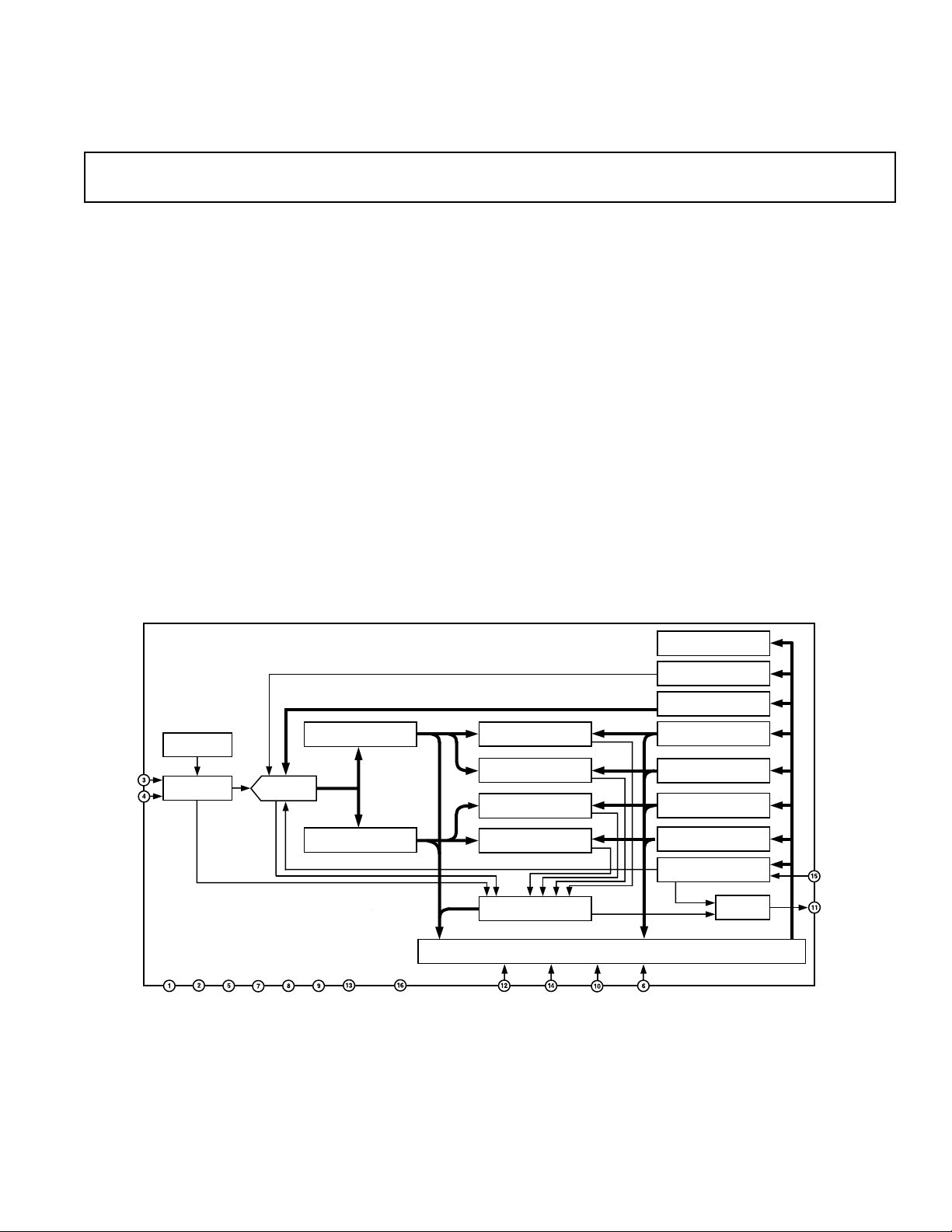
D+
D–
ON-CHIP TEMP.
SENSOR
ANALOG MUX
EXTERNAL DIODE OPEN-CIRCUIT
ADM1021A
NC
NC GND NC NC
V
DD
LOCAL TEMPERATURE
VALUE REGISTER
A-TO-D
CONVERTER
BUSY RUN/STANDBY
REMOTE TEMPERATURE
VALUE REGISTER
GND
FUNCTIONAL BLOCK DIAGRAM
LOCAL TEMPERATURE
LOW LIMIT COMPARATOR
LOCAL TEMPERATURE
HIGH LIMIT COMPARATOR
REMOTE TEMPERATURE
LOW LIMIT COMPARATOR
REMOTE TEMPERATURE
HIGH LIMIT COMPARATOR
STATUS REGISTER
SMBUS INTERFACE
NC
SDATA
SCLK ADD0 ADD1
ADDRESS POINTER
REGISTER
ONE-SHOT
REGISTER
CONVERSION RATE
REGISTER
LOCAL TEMPERATURE
LOW LIMIT REGISTER
LOCAL TEMPERATURE
HIGH LIMIT REGISTER
REMOTE TEMPERATURE
LOW LIMIT REGISTER
REMOTE TEMPERATURE
HIGH LIMIT REGISTER
CONFIGURATION
REGISTER
INTERRUPT
MASKING
NC = NO CONNECT
STBY
ALERT
*Patents Pending.
Pentium is a registered trademark of Intel Corporation.
REV. A
Information furnished by Analog Devices is believed to be accurate and
reliable. However, no responsibility is assumed by Analog Devices for its
use, nor for any infringements of patents or other rights of third parties that
may result from its use. No license is granted by implication or otherwise
under any patent or patent rights of Analog Devices.
One Technology Way, P.O. Box 9106, Norwood, MA 02062-9106, U.S.A.
Tel: 781/329-4700 www.analog.com
Fax: 781/326-8703 © Analog Devices, Inc., 2001

ADM1021A–SPECIFICATIONS
(TA = T
MIN
1
to T
, VDD = 3.0 V to 3.6 V, unless otherwise noted.)
MAX
Parameter Min Typ Max Unit Test Conditions/Comments
POWER SUPPLY AND ADC
Temperature Resolution 1 °C Guaranteed No Missed Codes
Temperature Error, Local Sensor ± 1 °C
–3 +3 °C
Temperature Error, Remote Sensor –3 +3 °CT
= 60°C to 100°C
A
–5 +5 °C
Supply Voltage Range 3 3.6 V Note 2
Undervoltage Lockout Threshold 2.5 2.7 2.95 V V
Undervoltage Lockout Hysteresis 25 mV
Power-On Reset Threshold 0.9 1.7 2.2 V VDD, Falling Edge
Input, Disables ADC, Rising Edge
DD
3
POR Threshold Hysteresis 50 mV
Standby Supply Current 1 5 µAV
= 3.3 V, No SMBus Activity
DD
4 µA SCLK at 10 kHz
Average Operating Supply Current 130 200 µA 0.25 Conversions/Sec Rate
Autoconvert Mode, Averaged Over 4 Seconds 225 330 µA Two Conversions/Sec Rate
Conversion Time 65 115 170 ms From Stop Bit to Conversion Complete
(Both Channels)
D+ Forced to D– + 0.65 V
Remote Sensor Source Current 120 205 300 µA High Level (Note 3)
71216µA Low Level (Note 3)
D-Source Voltage 0.7 V
Address Pin Bias Current (ADD0, ADD1) 50 µA Momentary at Power-On Reset
SMBUS INTERFACE
Logic Input High Voltage, V
IH
2.2 V VDD = 3 V to 5.5 V
STBY, SCLK, SDATA
Logic Input Low Voltage, V
IL
0.8 V VDD = 3 V to 5.5 V
STBY, SCLK, SDATA
SMBus Output Low Sink Current 6 mA SDATA Forced to 0.6 V
ALERT Output Low Sink Current 1 mA ALERT Forced to 0.4 V
Logic Input Current, I
, I
IH
IL
–1 +1 µA
SMBus Input Capacitance, SCLK, SDATA 5 pF
SMBus Clock Frequency 100 kHz
SMBus Clock Low Time, t
SMBus Clock High Time, t
SMBus Start Condition Setup Time, t
LOW
HIGH
SU:STA
4.7 µst
4 µst
4.7 µs
Between 10% Points
LOW
Between 90% Points
HIGH
SMBus Repeat Start Condition 250 ns Between 90% and 90% Points
Setup Time, t
SMBus Start Condition Hold Time, t
SMBus Stop Condition Setup Time, t
SU:STA
HD:STA
SU:STO
4 µs Time from 10% of SDATA to 90% of SCLK
4 µs Time from 90% of SCLK to 10% of SDATA
SMBus Data Valid to SCLK 250 ns Time from 10% or 90% of SDATA to 10%
Rising Edge Time, t
SU:DAT
SMBus Data Hold Time, t
SMBus Bus Free Time, t
BUF
HD:DAT
0 µs
4.7 µs Between Start/Stop Condition
of SCLK
SCLK Falling Edge to SDATA 1 µs Master Clocking in Data
Valid Time, t
NOTES
1
T
= 100°C; T
MAX
2
Operation at VDD = 5 V guaranteed by design, not production tested.
3
Guaranteed by design, not production tested.
Specifications subject to change without notice.
MIN
VD,DAT
= 0°C.
–2–
REV. A

ADM1021A
TOP VIEW
(Not to Scale)
NC = NO CONNECT
NC
V
DD
D+
D–
NC
ADD1
GND
GND
NC
STBY
SCLK
NC
SDATA
ALERT
ADD0
NC
ADM1021A
16
15
14
13
12
11
10
9
1
2
3
4
5
6
7
8
ABSOLUTE MAXIMUM RATINGS*
Positive Supply Voltage (VDD) to GND . . . . . . –0.3 V to +6 V
D+, ADD0, ADD1 . . . . . . . . . . . . . . . –0.3 V to V
+ 0.3 V
DD
D– to GND . . . . . . . . . . . . . . . . . . . . . . . . . . –0.3 V to +0.6 V
SCLK, SDATA, ALERT, STBY . . . . . . . . . . . –0.3 V to +6 V
Input Current . . . . . . . . . . . . . . . . . . . . . . . . . . . . . . . ±50 mA
Input Current, D– . . . . . . . . . . . . . . . . . . . . . . . . . . . . ± 1 mA
ESD Rating, All Pins (Human Body Model) . . . . . . . . 2000 V
Continuous Power Dissipation
Up to 70°C . . . . . . . . . . . . . . . . . . . . . . . . . . . . . . 650 mW
Derating above 70°C . . . . . . . . . . . . . . . . . . . . . 6.7 mW/°C
Operating Temperature Range . . . . . . . . . . –55°C to +125°C
Maximum Junction Temperature (T
max) . . . . . . . . . . 150°C
J
Storage Temperature Range . . . . . . . . . . . . –65°C to +150°C
Lead Temperature, (Soldering 10 sec) . . . . . . . . . . . . . 300°C
IR Reflow Peak Temperature . . . . . . . . . . . . . . . . . . . . . 220°C
*Stresses above those listed under Absolute Maximum Ratings may cause perma-
nent damage to the device. This is a stress rating only; functional operation of the
device at these or any other conditions above those indicated in the operational
section of this specification is not implied. Exposure to absolute maximum rating
conditions for extended periods may affect device reliability.
THERMAL CHARACTERISTICS
16-Lead QSOP Package: θ
= 150°C/W.
JA
ORDERING GUIDE
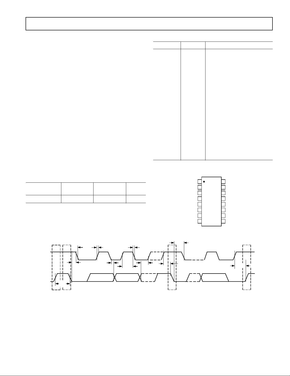
PIN FUNCTION DESCRIPTIONS
Pin No. Mnemonic Description
1, 5, 9, 13, 16 NC No Connect
2V
DD
Positive Supply, 3 V to 5.5 V.
3 D+ Positive Connection to Remote
Temperature Sensor.
4 D– Negative Connection to Remote
Temperature Sensor.
6 ADD1 Three-State Logic Input, Higher
Bit of Device Address.
7, 8 GND Supply 0 V Connection.
10 ADD0 Three-State Logic Input, Lower
Bit of Device Address.
11 ALERT Open-Drain Logic Output Used as
Interrupt or SMBus Alert.
12 SDATA Logic Input/Output, SMBus Serial
Data. Open-Drain Output.
14 SCLK Logic Input, SMBus Serial Clock.
15 STBY Logic Input Selecting Normal
Operation (High) or Standby Mode
(Low).
PIN CONFIGURATION
Temperature Package Package
Model Range Description Option
ADM1021AARQ 0°C to 100°C 16-Lead QSOP RQ-16
t
R
t
HD;DAT
t
HIGH
SCL
SDA
t
LOW
t
HD;STA
t
BUF
S
P
Figure 1. Diagram for Serial Bus Timing
t
F
t
SU;DAT
t
SU;STA
t
HD;STA
t
SU;STO
PS
REV. A
–3–

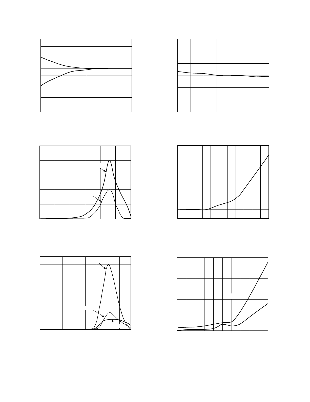
ADM1021A–Typical Performance Characteristics
20
15
10
5
0
–5
–10
–15
TEMPERATURE ERROR – ⴗC
–20
–25
–30
Figure 2. Temperature Error vs. PC Board Track Resistance
D+ TO GND
D+ TO V
DD
LEAKAGE RESISTANCE – M⍀
101
100
Figure 5. Temperature Error of ADM1021A vs.
Pentium III Temperature
2
1
ERROR – ⴗC
–1
–2
–3
60070
50
80
TEMPERATURE – ⴗC
UPPER SPEC LEVEL
DEV10
LOWER SPEC LEVEL
90
100
110
120
5
4
250mV p-p REMOTE
3
2
TEMPERATURE ERROR – ⴗC
1
0
100
100mV p-p REMOTE
FREQUENCY – Hz
100M1k 10k 100k 1M 10M
Figure 3. Temperature Error vs. Power Supply Noise
Frequency
9
8
7
6
5
4
3
TEMPERATURE ERROR – ⴗC
2
1
0
10 1k 10k
1
100 100k 1M
100mV p-p
50mV p-p
FREQUENCY – Hz
25mV p-p
10M 100M
Figure 4. Temperature Error vs. Common-Mode Noise
Frequency
14
12
10
8
6
4
2
TEMPERATURE ERROR – ⴗC
0
–1
2
4 6 81012141618202224
CAPACITANCE – nF
Figure 6. Temperature Error vs. Capacitance Between
D+ and D–
70
60
50
40
30
20
SUPPLY CURRENT – A
10
0
1
5 10 25 50 75 100 1000250 500 750
SCLK FREQUENCY – kHz
VDD = 3.3V
VDD = 5V
Figure 7. Standby Supply Current vs. Clock Frequency
–4–
REV. A
 Loading...