Analog Devices ADM101E Datasheet

Craft Port
TM
Tiny RS-232 Transceiver for
a
FEATURES
460 kbit/s Transmission Rate
Single +5 V Power Supply
Compatible with RS-232 Input/Output Levels
0.1 F Charge Pump Capacitors
One Driver and One Receiver
On-Board DC-DC Converter
ⴞ4.2 V Output Swing with +5 V Supply
Low Power BiCMOS: 500 A I
Ultralow Power (1 A) Shutdown Mode
10-Lead SOIC Package
APPLICATIONS
Mobile Telephones
Palmtop Computers
PDAs
Portable Instrumentation
GPS Receivers
CC
Portable Applications
ADM101E
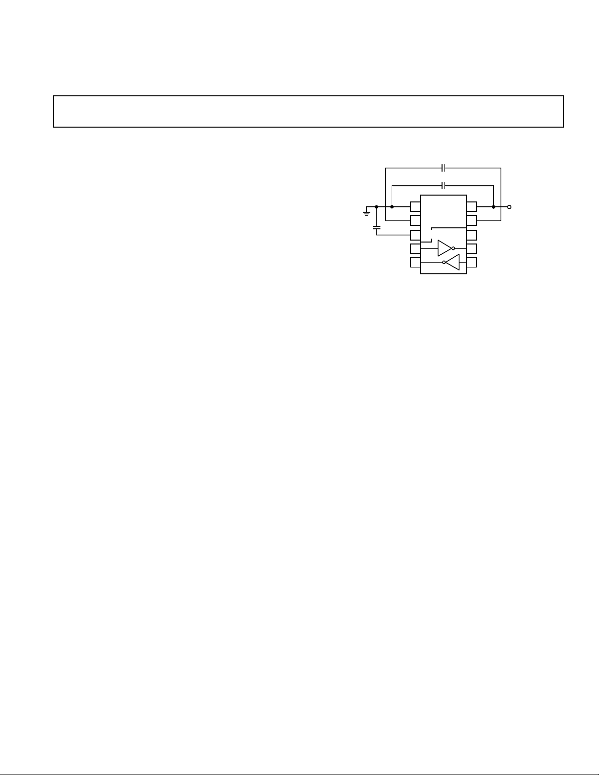
FUNCTIONAL BLOCK DIAGRAM
0.1mF
+
0.1mF
+
V
CC
10
C1+
9
8
SD
T
7
OUT
R
R1
6
IN
0.1mF
GND
C1–
+
R
OUT
+5V TO –5V
1
VOLTAGE
INVERTER
2
V–
ADM101E
3
T
IN
T1
4
5
+5V
GENERAL DESCRIPTION
The ADM101E is a single channel RS-232 driver and receiver in
the Analog Devices Craft Port
series, designed to operate from a
single, +5 V supply. A highly efficient charge-pump voltage
inverter generates an on-chip –5 V supply, which eliminates the
need for a negative power supply for the driver and permits
RS-232 compatible output levels to be developed using charge
pump capacitors as small as 0.1 µF.
A shutdown input disables the charge pump and puts the device
into a low power shutdown mode, in which the current con-
sumption is typically less than 1 µA. The transmitter is disabled
during shutdown but the receiver remains functional.
Craft Port is a trademark of Analog Devices, Inc.
An epitaxial BiCMOS construction minimizes power consumption to 3 mW and also guards against latch-up. Overvoltage
protection is provided allowing the receiver inputs to withstand
continuous voltages in excess of ±30 V. In addition, all I-O pins
have ESD protection to levels greater than 15 kV.
The ADM101E is available in a 10-lead µSOIC package, which
makes it ideal for serial communications in small, portable applications such as palmtop computers and mobile telephones,
where a full, RS-232 serial interface is not required, but compact size and low power drain are paramount.
REV. 0
Information furnished by Analog Devices is believed to be accurate and
reliable. However, no responsibility is assumed by Analog Devices for its
use, nor for any infringements of patents or other rights of third parties
which may result from its use. No license is granted by implication or
otherwise under any patent or patent rights of Analog Devices.
One Technology Way, P.O. Box 9106, Norwood, MA 02062-9106, U.S.A.
Tel: 781/329-4700 World Wide Web Site: http://www.analog.com
Fax: 781/326-8703 © Analog Devices, Inc., 1999

ADM101E–SPECIFICATIONS
(VCC = +5 V ⴞ 10%, C1 = C2 = 0.1 F. All specifications T
otherwise noted.)
MIN
Parameter Min Typ Max Units Test Conditions/Comments
Output Voltage Swing ±3.5 ±4.2 V V
±3.25 ±4.2 V V
= 5 V ±5%, T
CC
= 5 V ±10%, T
CC
Loaded with 3 kΩ to GND
OUT
Loaded with 3 kΩ to
OUT
GND
Power Supply Current (Unloaded) 0.5 1 mA No Load, TIN = VCC or GND
V
CC
V
Power Supply Current (Loaded) 1.85 2.5 mA T
CC
Power Supply Current (Shutdown) 1 µA SD Input = V
V
CC
Input Logic Threshold Low, V
Input Logic Threshold High, V
INL
INH
2.4 V
0.8 V
Loaded with 3 kΩ to GND
OUT
CC
Input Leakage Current ±1 µA
RS-232 Input Voltage Range –15 +15 V
RS-232 Input Threshold Low 0.8 2.2 V
RS-232 Input Threshold High 2.4 2.6 V
RS-232 Input Hysteresis 0.2 V
RS-232 Input Resistance 357kΩ
TTL/CMOS Output Voltage Low, V
TTL/CMOS Output Voltage High, V
Propagation Delay 0.25 µs RS-232 to TTL
Instantaneous Slew Rate
1
OL
OH
3.5 V I
25 V/µsC
0.4 V I
Transition Region Slew Rate 11 V/µsR
= 1.6 mA
OUT
= –1.0 mA
OUT
= 10 pF, R
L
= 3 kΩ, C
L
= 3 kΩ–7 kΩ, TA = +25°C
L
= 1000 pF
L
Measured from +3 V to –3 V or Vice Versa
Baud Rate 460 kB R
Output Resistance 300 Ω V
= 3 kΩ, C
L
= 0 V, V
CC
= 1 nF
L
= ±2 V
OUT
RS-232 Output Short Circuit Current ±25 ±60 mA
NOTES
1
Sample tested to ensure compliance.
Specifications subject to change without notice.
to T
MAX
unless
ABSOLUTE MAXIMUM RATINGS*
(T
= +25°C unless otherwise noted)
A
VCC . . . . . . . . . . . . . . . . . . . . . . . . . . . . . . . . . . . . . . . . . +6 V
V– . . . . . . . . . . . . . . . . . . . . . . . . . . . . . . . . . . +0.3 V to –6 V
Input Voltages
Driver Input T
Receiver Input R
. . . . . . . . . . . . . . –0.3 V to (VCC, +0.3 V)
IN
. . . . . . . . . . . . . . . . . . . . . . . . . . . ±30 V
IN
Output Voltages
Driver Output T
Receiver Output R
. . . . . . . . (VCC, +0.3 V) to (V–, –0.3 V)
OUT
. . . . . . . . . . . –0.3 V to (VCC +0.3 V)
OUT
Short Circuit Duration
T
. . . . . . . . . . . . . . . . . . . . . . . . . . . . . . . . . Continuous
OUT
Power Dissipation
RM-10 (Derate 12 mW/°C Above +70°C) . . . . . . . 1488 mW
Thermal Impedance . . . . . . . . . . . . . . . . . . . . . . . +135°C/W
Operating Temperature Range
Industrial (A Version) . . . . . . . . . . . . . . . . –40°C to +85°C
Storage Temperature Range . . . . . . . . . . . . –65°C to +150°C
Lead Temperature Soldering
Vapor Phase (60 sec) . . . . . . . . . . . . . . . . . . . . . . . .+215°C
Infrared (15 sec) . . . . . . . . . . . . . . . . . . . . . . . . . . . .+220°C
ESD Rating . . . . . . . . . . . . . . . . . . . . . . . . . . . . . . . . >2000 V
ESD Rating (I-O Pins) . . . . . . . . . . . . . . . . . . . . . . . . . 15 kV
*This is a stress rating only; functional operation of the device at these or any other
conditions above those indicated in the operation sections of this specification is
not implied. Exposure to absolute maximum rating conditions for extended
periods of time may affect reliability.
ORDERING GUIDE
Temperature Package Package
Model Range Description Option
ADM101EARM –40°C to +85°C µSOIC RM-10
–2–
REV. 0
 Loading...