ANALOG DEVICES ADL5812 Service Manual
Dual High IP3, 700 MHz to 2800 MHz, Double Balanced,
V
Passive Mixer, IF Amplifier, and Wideband LO Amplifier
FEATURES
RF frequency: 700 MHz to 2800 MHz continuous
LO frequency: 250 MHz to 2800 MHz, high-side or
low-side inject
IF range: 30 MHz to 450 MHz
Power conversion gain of 6.7 dB at 1900 MHz
SSB noise figure of 11.6 dB at 1900 MHz
Input IP3 of 27.2 dBm at 1900 MHz
Input P1dB of 12.5 dBm at 1900 MHz
Typical LO drive of 0 dBm
Single-ended, 50 Ω RF port
Single-ended or balanced LO input port
Single-supply operation: 3.6 V to 5.0 V
Serial port interface control on all functions
Exposed paddle 6 mm × 6 mm, 40-lead LFCSP package
APPLICATIONS
Multiband/multistandard cellular base station diversity
receivers
Wideband radio link diversity downconverters
Multimode cellular extenders and broadband receivers
ADL5812
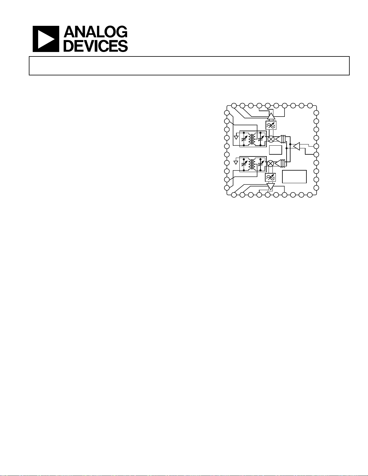
FUNCTIONAL BLOCK DIAGRAM
VPIF1
IFGM1
NC
IFOP1
IFON1
NC
IFGD1
V1LO4V1LO3
2LO4V2LO3V2LO2
V1LO2
30
V1LO1
29
NC
28
NC
27
NC
26
LOIP
25
LOIN
24
LE
DATA
23
CLK
22
V2LO1
21
09913-001
40 39 38 37 36 35 34 33 32 31
1
RF1
2
RFCT1
IFON2
BIAS
GEN
ADL5812
INTERFACE
NC
IFGD2
SERIAL
PORT
NC
NC
NC
NC
NC
NC
RFCT2
RF2
3
4
5
6
7
8
9
10
11 12 13 14 15 16 17 18 19 20
NC
VPIF2
IFOP2
IFGM2
Figure 1.
GENERAL DESCRIPTION
The ADL5812 uses revolutionary new broadband, square wave
limiting, local oscillator (LO) amplifiers to achieve an
unprecedented radio frequency (RF) bandwidth of 700 MHz
to 2800 MHz. Unlike conventional narrow-band sine wave LO
amplifier solutions, this permits the LO to be applied either
above or below the RF input over an extremely wide bandwidth.
Because energy storage elements are not used, the dc current
consumption also decreases with decreasing LO frequency.
The ADL5812 uses highly linear, doubly balanced, passive mixer
cores along with integrated RF and LO balancing circuits to
allow single-ended operation. The ADL5812 incorporates
programmable RF baluns, allowing optimal performance over
a 700 MHz to 2800 MHz RF input frequency. The balanced
passive mixer arrangement provides outstanding LO-to-RF and
LO-to-IF leakages, excellent RF-to-IF isolation, and excellent
intermodulation performance over the full RF bandwidth.
The balanced mixer cores also provide extremely high input
linearity, allowing the device to be used in demanding
wideband applications where in-band blocking signals may
otherwise result in the degradation of dynamic range. Blocker
noise figure performance is comparable to narrow-band passive
mixer designs. High linearity IF buffer amplifiers follow the
passive mixer cores, yielding typical power conversion gains of
6.7 dB, and can be used with a wide range of output
impedances. For low voltage applications, the ADL5812 is
capable of operation at voltages down to 3.6 V with
substantially reduced current. Two logic bits are provided to
individually power down (1.5 mA for both channels) the two
channels as desired.
All features of the ADL5812 are controlled via a 3-wire serial
port interface, resulting in optimum performance and
minimum external components.
The ADL5812 is fabricated using a BiCMOS high performance
IC process. The device is available in a 40-lead, 6mm × 6mm,
LFCSP package and operates over a −40°C to +85°C
temperature range. An evaluation board is also available.
Rev. 0
Information furnished by Analog Devices is believed to be accurate and reliable. However, no
responsibility is assumed by Anal og Devices for its use, nor for any infringements of patents or ot her
rights of third parties that may result from its use. Specifications subject to change without notice. No
license is granted by implication or otherwise under any patent or patent rights of Analog Devices.
Trademarks and registered trademarks are the property of their respective owners.
One Technology Way, P.O. Box 9106, Norwood, MA 02062-9106, U.S.A.
Tel: 781.329.4700 www.analog.com
Fax: 781.461.3113 ©2011 Analog Devices, Inc. All rights reserved.

ADL5812
TABLE OF CONTENTS
Features.............................................................................................. 1
Applications....................................................................................... 1
Functional Block Diagram .............................................................. 1
General Description ......................................................................... 1
Revision History ............................................................................... 2
Specifications..................................................................................... 3
Timing Characteristics ................................................................ 4
Absolute Maximum Ratings............................................................ 5
ESD Caution.................................................................................. 5
Pin Configuration and Function Descriptions............................. 6
Typical Performance Characteristics ............................................. 7
3.6 V Performance...................................................................... 16
Spurious Performance................................................................ 17
Circuit Description......................................................................... 20
RF Subsystem.............................................................................. 20
LO Subsystem ............................................................................. 21
Applications Information.............................................................. 22
Basic Connections...................................................................... 22
IF Port.......................................................................................... 22
Bias Resistor Selection ............................................................... 22
VGS Programming..................................................................... 23
Low-Pass Filter Programming.................................................. 23
RF Balun Programming ............................................................ 23
Register Structure........................................................................... 24
Evaluation Board............................................................................ 25
Outline Dimensions....................................................................... 27
Ordering Guide .......................................................................... 27
REVISION HISTORY
7/11—Revision 0: Initial Version
Rev. 0 | Page 2 of 28

ADL5812
SPECIFICATIONS
VS = 5 V, TA = 25°C, fRF = 1900 MHz, fLO = 1697 MHz, RF power = −10 dBm, LO power = 0 dBm, R1 = R2 = 1200 Ω, ZO = 50 Ω, optimum
SPI settings, unless otherwise noted.
Table 1.
Parameter Test Conditions/Comments Min Typ Max Unit
RF INPUT INTERFACE
Return Loss Tunable to >20 dB broadband via serial port 10 dB
Input Impedance 50 Ω
RF Frequency Range 700 2800 MHz
OUTPUT INTERFACE
Output Impedance Differential impedance, f = 200 MHz 260||1.2 Ω||pF
IF Frequency Range 30 450 MHz
DC Bias Voltage1 Externally generated VS V
LO INTERFACE
LO Power −6 0 +10 dBm
Return Loss 13.3 dB
Input Impedance 50 Ω
LO Frequency Range Low-side or high-side LO 250 2800 MHz
DYNAMIC PERFORMANCE
Power Conversion Gain Including 4:1 IF port transformer and PCB loss 6.7 dB
Voltage Conversion Gain Z
SSB Noise Figure 11.6 dB
SSB Noise Figure Under Blocking
Input Third-Order Intercept
Input Second-Order Intercept
Input 1 dB Compression Point 12.5 dBm
LO-to-IF Output Leakage Unfiltered IF output −37 dBm
LO-to-RF Input Leakage −46 dBm
RF-to-IF Output Isolation 26 dB
IF/2 Spurious −10 dBm input power −70 dBc
IF/3 Spurious −10 dBm input power −78 dBc
POWER INTERFACE
Supply Voltage, VS 3.6 5 5.5 V
Quiescent Current Resistor programmable IF current 412 mA
Power-Down Current 1.5 mA
1
Supply voltage must be applied from external circuit through choke inductors.
= 50 Ω, differential Z
SOURCE
= 200 Ω differential 13.1 dB
LOAD
5 dBm blocker present ±10 MHz from wanted RF input,
LO source filtered
= 1900 MHz, f
f
RF1
= 1901 MHz, fLO = 1697 MHz, each RF tone
RF2
at −10 dBm
= 1900 MHz, f
f
RF1
= 2000 MHz, fLO = 1697 MHz, each RF tone
RF2
at −10 dBm
21 dB
27.2 dBm
55 dBm
Rev. 0 | Page 3 of 28
ADL5812
A
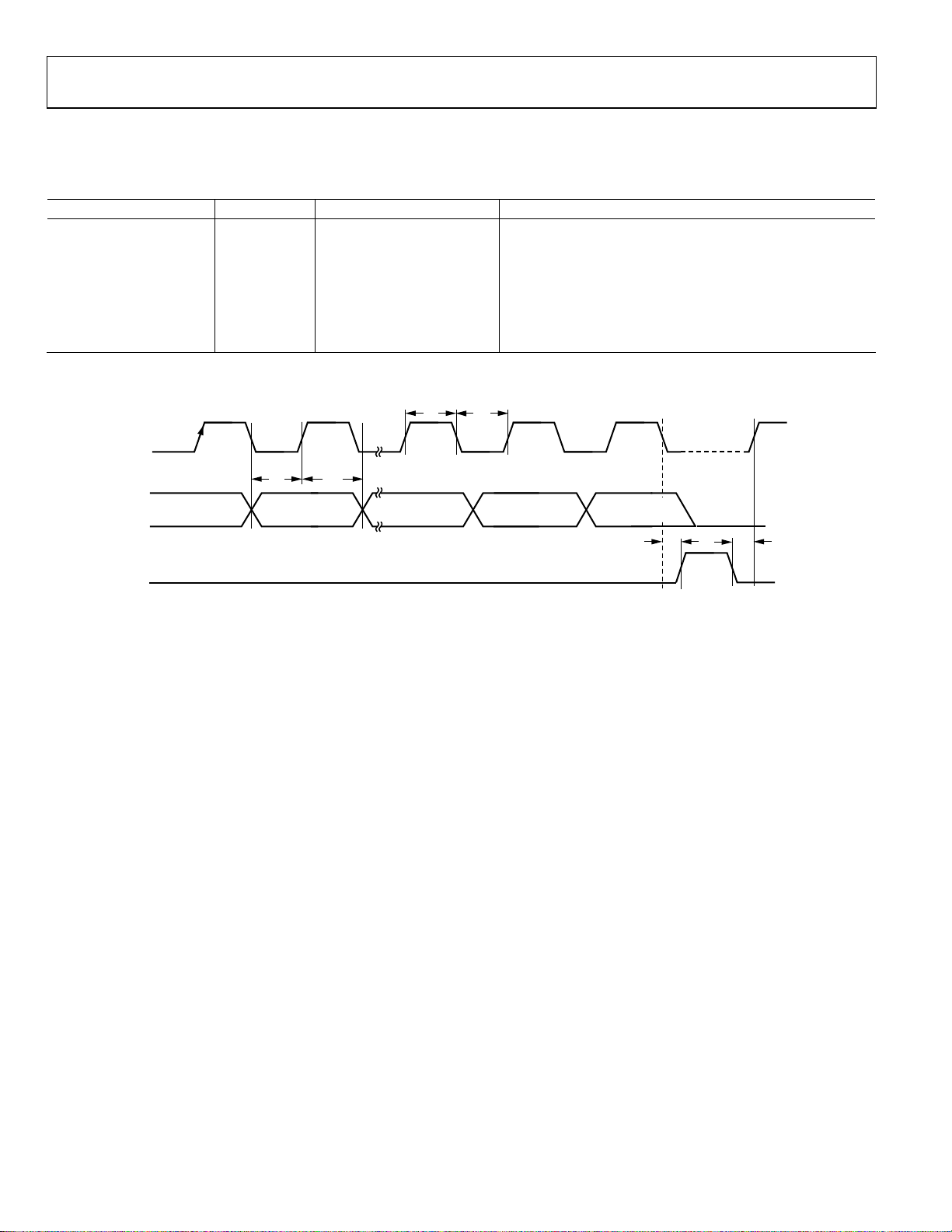
TIMING CHARACTERISTICS
Low logic level ≤ 0.4 V, and high logic level ≥ 1.4 V.
Table 2. Serial Interface Timing
Parameter Limit Unit Test Conditions/Comments
t1 20 ns minimum LE setup time
t2 10 ns minimum DATA-to-CLK setup time
t3 10 ns minimum DATA-to-CLK hold time
t4 25 ns minimum CLK high duration
t5 25 ns minimum CLK low duration
t6 10 ns minimum CLK-to-LE setup time
t7 20 ns minimum LE pulse width
Timing Diagram
CLK
t
4
t
5
t
2
D
DB23 (MSB) DB22
TA
LE
t
3
DB2 DB1
(CONTROL BIT C2)(CONTROL BIT C3)
DB0 (LSB)
(CONTROL BIT C1)
t
t
t
7
6
1
09913-002
Figure 2. Timing Diagram
Rev. 0 | Page 4 of 28
ADL5812
ABSOLUTE MAXIMUM RATINGS
Table 3.
Parameter Rating
Supply Voltage, V
CLK, DATA, LE 5.5 V
IF Output Bias 6.0 V
RF Input Power 20 dBm
LO Input Power 13 dBm
Internal Power Dissipation 2.5 W
θJA (Exposed Paddle Soldered Down) 30°C
Maximum Junction Temperature 150°C
Operating Temperature Range −40°C to +85°C
Storage Temperature Range −65°C to +150°C
5.5 V
POS
Stresses above those listed under Absolute Maximum Ratings
may cause permanent damage to the device. This is a stress
rating only; functional operation of the device at these or any
other conditions above those indicated in the operational
section of this specification is not implied. Exposure to absolute
maximum rating conditions for extended periods may affect
device reliability.
ESD CAUTION
Rev. 0 | Page 5 of 28
ADL5812
2
2
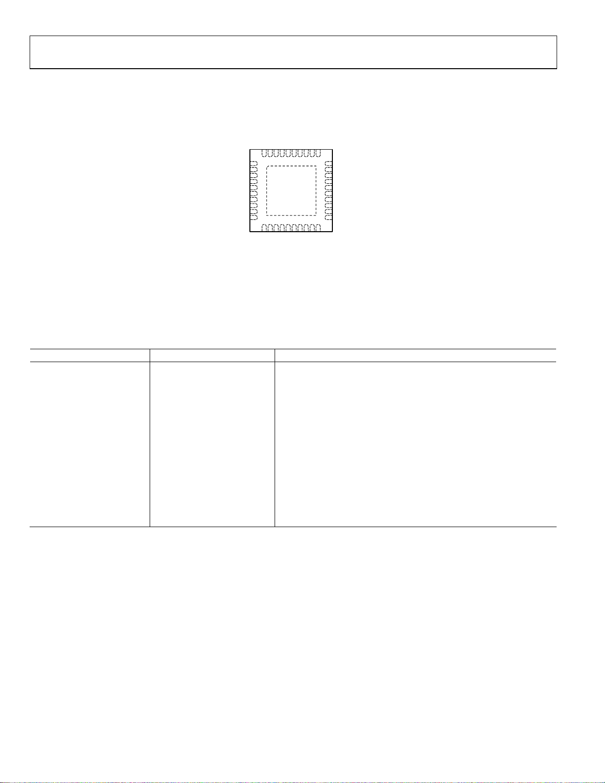
PIN CONFIGURATION AND FUNCTION DESCRIPTIONS
VPIF1
IFGM1NCIFOP1
IFON1NCIFGD1
V1LO4V1LO3V1LO
32
31
33
34
35
36
37
38
39
40
1
RF1
RFCT1
2
NC
3
NC
4
NC
5
6
NC
NC
7
NC
8
9
RFCT2
RF2
10
NOTES
1. NC = NO CONNE CT. CAN BE GRO UNDED.
. EXPOSE D PAD MUST BE CO NNECTED
TO GROUND.
ADL5812
TOP VIEW
(Not to Scale)
11
12
13
15
14
NC
VPIF2
IFOP2
IFON2NCIFGD2
IFGM2
17
16
Figure 3. Pin Configuration
30
V1LO1
29
NC
28
NC
NC
27
26
LOIP
25
LOIN
LE
24
23
DATA
22
CLK
21
V2LO1
18
19
20
V2LO4
V2LO3
V2LO2
09913-003
Table 4. Pin Function Descriptions
Pin No. Mnemonic Description
1, 10 RF1, RF2 RF Input. Should be ac-coupled.
2, 9 RFCT1, RFCT2 RF Balun Center Tap (AC Ground).
3 to 8, 13, 16, 27 to 29, 35, 38 NC No Connect. Can be grounded.
11, 40 VPIF1, VPIF2 Supply Voltage for IF Amplifier.
12, 39 IFGM1, IFGM2 IF Amplifier Bias Control.
14, 15, 36, 37 IFOP1, IFOP2, IFON1, IFON2
Differential Open-Collector IF Outputs. Should be pulled up to V
external inductors.
17, 34 IFGD1, IFGD2 Supply Return for IF Amplifier. Must be grounded.
18 to 21, 30 to 33
V1LO1, V1LO2, V1LO3, V1LO4,
Positive Supply Voltages for LO Amplifiers.
V2LO1, V2LO2, V2LO3, V2LO4
22, 23, 24 CLK, DATA, LE Serial Port Interface Control.
25 LOIN Ground Return for LO Input. Must be ac coupled.
26 LOIP LO Input. Should be ac-coupled.
EPAD Exposed pad must be connected to ground.
CC
via
Rev. 0 | Page 6 of 28
ADL5812
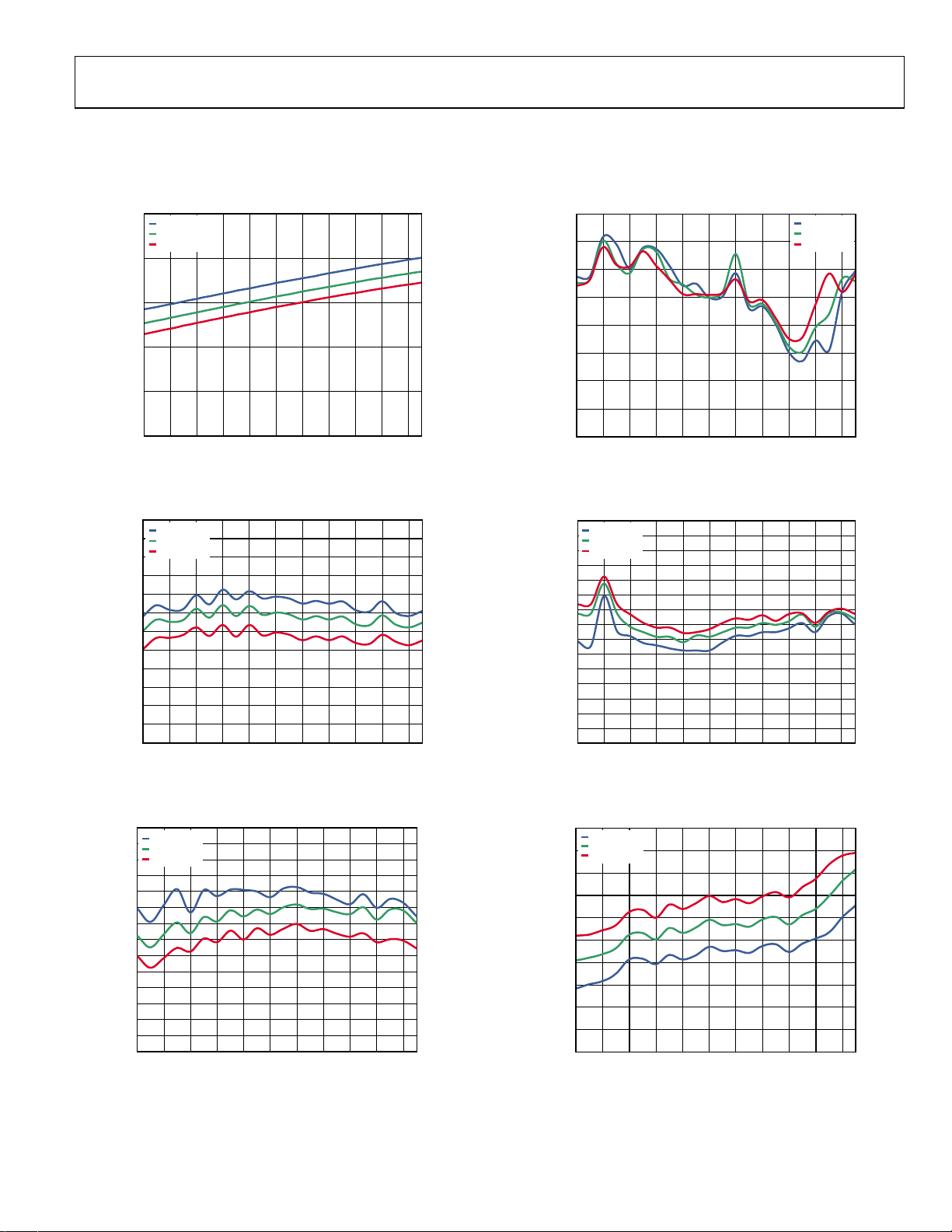
TYPICAL PERFORMANCE CHARACTERISTICS
VS = 5 V, TA = 25°C, fRF = 1900 MHz, fLO = 1697 MHz, RF power = −10 dBm, LO power = 0 dBm, R1 = R2 = 1200 Ω, ZO = 50 Ω, optimum
SPI settings, unless otherwise noted.
450
400
TA = –40°C
= +25°C
T
A
=+85°C
T
A
70
65
60
TA = –40°C
= +25°C
T
A
=+85°C
T
A
350
300
SUPPLY CURRENT (mA)
250
200
700 900 1100 1300 1500 1700 1900 2100 2300 2500 2700
RF FREQ UENCY (MHz )
Figure 4. Supply Current vs. RF Frequency
12
TA = –40°C
11
= +25°C
T
A
=+85°C
T
A
10
9
8
7
6
5
4
CONVERSION GAIN (dB)
3
2
1
0
700 900 1100 1300 1500 1700 1900 2100 2300 2500 2700
RF FREQUE NCY (MHz)
Figure 5. Power Conversion Gain vs. RF Frequency
32
TA = –40°C
31
= +25°C
T
A
T
=+85°C
30
A
29
28
27
26
25
24
23
INPUT IP3 (dBm)
22
21
20
19
18
700 900 1100 1300 1500 1700 1900 2100 2300 2500 2700
RF FREQUENCY (MHz)
Figure 6. Input IP3 vs. RF Frequency
55
50
45
INPUT IP2 (dBm)
40
35
30
700 900 1100 1300 1500 1700 1900 2100 2300 2500 2700
09913-008
RF FREQUENCY (MHz)
09913-016
Figure 7. Input IP2 vs. RF Frequency
20
TA =–40°C
19
= +25°C
T
A
18
=+85°C
T
A
17
16
15
14
13
12
11
10
INPUT P1dB (dBm)
9
8
7
6
5
700 900 1100 1300 1500 1700 1900 2100 2300 2500 2700
09913-011
RF FREQ UENCY (MHz)
09913-020
Figure 8. Input P1dB vs. RF Frequency
16
TA = –40°C
= +25°C
T
A
15
T
= +85°C
A
14
13
12
11
10
9
SSB NOISE FIGURE (dB)
8
7
6
700 900 1100 1300 1500 1700 1900 2100 2300 2500 2700
09913-019
RF FREQUENCY (MHz)
09913-025
Figure 9. SSB Noise Figure vs. RF Frequency
Rev. 0 | Page 7 of 28
ADL5812
450
400
350
300
SUPPLY CURRENT (mA)
250
200
–40 –20 0 20 40 60 80
TEMPERAT URE (°C)
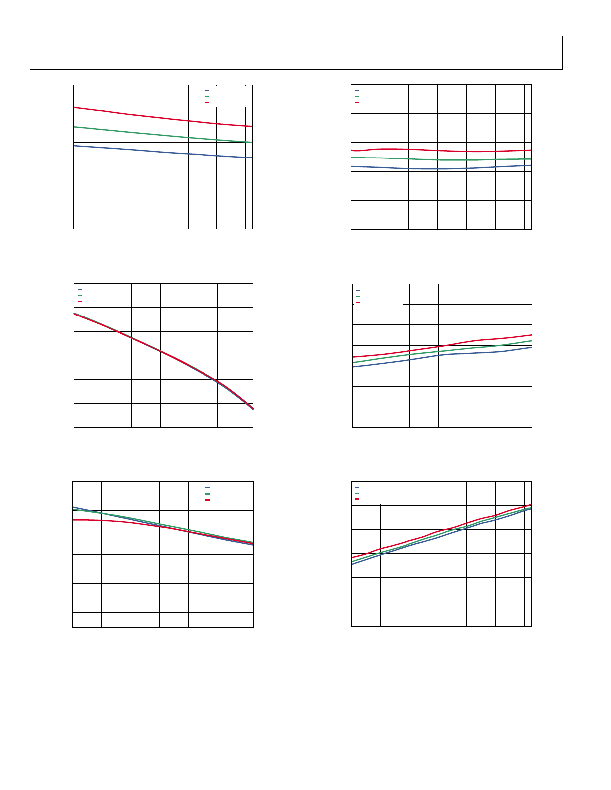
Figure 10. Supply Current vs. Temperature
8.0
V
= 4.75V
POS
= 5.00V
V
POS
= 5.25V
V
POS
7.5
V
V
V
POS
POS
POS
= 4.75V
= 5.00V
= 5.25V
09913-026
65
V
= 4.75V
POS
= 5.00V
V
POS
63
61
59
57
55
53
INPUT IP2 (dBm)
51
49
47
45
–40–200 20406080
= 5.25V
V
POS
TEMPERATURE (°C)
Figure 13. Input IP2 vs. Temperature
16
V
= 4.75V
POS
= 5.00V
V
POS
= 5.25V
V
POS
15
09913-029
7.0
6.5
6.0
CONVERSION GAIN (dB)
5.5
5.0
–40–200 20406080
TEMPERAT URE (°C)
Figure 11. Power Conversion Gain vs. Temperature
30
29
28
27
26
25
24
INPUT IP3 (dBm)
23
22
21
20
–40–200 20406080
TEMPERAT URE (°C)
V
= 4.75V
POS
V
= 5.00V
POS
V
= 5.25V
POS
Figure 12. Input IP3 vs. Temperature
14
13
12
INPUT P1dB (dBm)
11
10
9
–40–200 20406080
09913-027
TEMPERATURE (°C)
09913-030
Figure 14. Input P1dB vs. Temperature
14
V
= 4.75V
POS
= 5.00V
V
POS
= 5.25V
V
POS
13
12
11
10
SSB NOISE FIGURE (dB)
9
8
–40 –20 0 20 40 60 80
09913-028
TEMPERAT URE (°C)
09913-031
Figure 15. SSB Noise Figure vs. Temperature
Rev. 0 | Page 8 of 28
ADL5812
450
400
70
65
60
RF = 900MHz
RF = 1900MHz
RF = 2500MHz
350
300
SUPPLY CURRENT (mA)
250
RF = 900MHz
RF = 1900MHz
RF = 2500MHz
200
30 80 130 180 230 28 0 330 380 430
IF FREQUENCY (MHz)
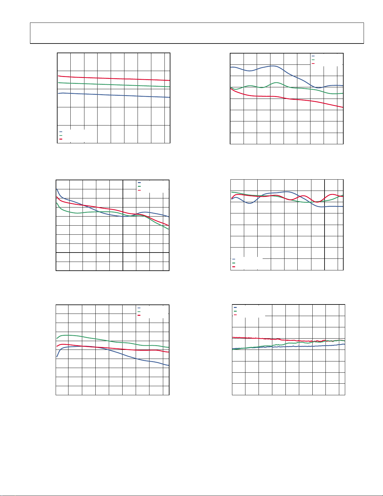
Figure 16. Supply Current vs. IF Frequency
10
9
8
7
6
5
4
3
CONVERSION GAIN (dB)
2
1
0
30 80 130 180 230 280 330 380 430
IF FRE QUENCY (MHz )
Figure 17. Power Conversion Gain vs. IF Frequency
35
33
31
29
27
25
23
21
INPUT IP3 (dBm)
19
17
15
30 80 130 180 230 280 33 0 380 430
IF FREQUENCY (MHz)
Figure 18. Input IP3 vs. IF Frequency
RF = 900MHz
RF = 1900MHz
RF = 2500MHz
RF = 900MHz
RF = 1900MHz
RF = 2500MHz
55
50
45
INPUT IP2 (dBm)
40
35
30
30 80 130 180 230 280 330 380 430
09913-032
IF FREQUENCY (MHz)
09913-035
Figure 19. Input IP2 vs. IF Frequency
16
14
12
10
8
6
INPUT P1dB (dBm)
4
2
RF = 900MHz
RF = 1900MHz
RF = 2500MHz
0
30 80 130 180 230 280 330 380 430
09913-033
IF FRE QUENCY (MHz )
09913-036
Figure 20. Input P1dB vs. IF Frequency
16
RF = 900MHz
RF = 1900MHz
RF = 2500MHz
14
12
10
8
6
SSB NOISE F IGURE (dB)
4
2
0
30 80 130 180 230 280 330 380 430
09913-034
IF FREQUENCY (MHz)
09913-037
Figure 21. SSB Noise Figure vs. IF Frequency
Rev. 0 | Page 9 of 28
 Loading...