

50 MHz to 6 GHz
FEATURES
Fixed gain of 15 dB
Operation up to 6 GHz
Input/output internally matched to 50 Ω
Integrated bias control circuit
Output IP3
44 dBm at 500 MHz
40 dBm at 900 MHz
Output 1 dB compression: 19.7 dBm at 900 MHz
Noise figure of 3.5 dB at 900 MHz
Single 5 V power supply
Small footprint 8-lead LFCSP
Pin compatible with 20 dB gain ADL5542
1 kV ESD (Class 1C)
GENERAL DESCRIPTION
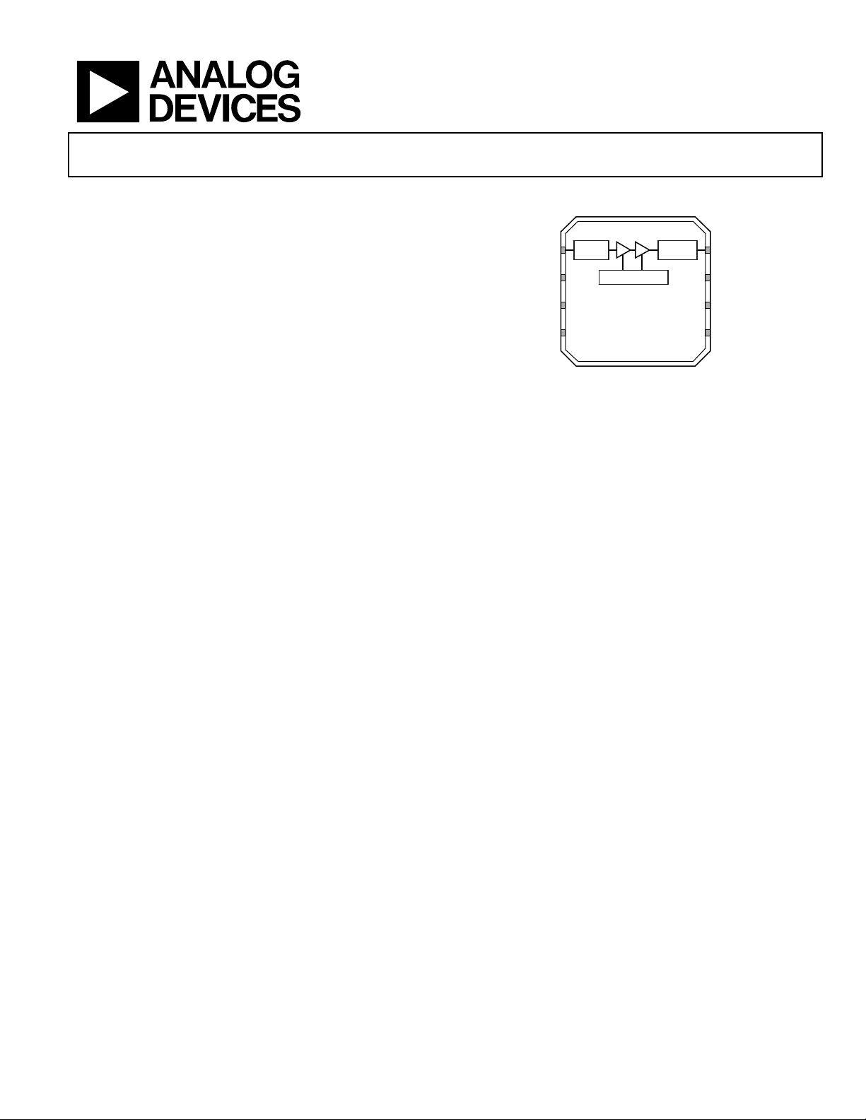
The ADL5541 is a broadband 15 dB linear amplifier that operates
at frequencies up to 6 GHz. The device can be used in a wide
variety of CATV, cellular, and instrumentation equipment.
The ADL5541 provides a gain of 15 dB, which is stable over
frequency, temperature, power supply, and from device to
device. The device is internally matched to 50 Ω with an input
return loss of 10 dB or better up to 6 GHz. Only input/output
ac coupling capacitors, power supply decoupling capacitors, and
an external inductor are required for operation.
RF/IF Gain Block
ADL5541
FUNCTIONAL BLOCK DIAGRAM
RFIN
GND
GND
CB
MATCH
2
3
4
BIAS CONTROL
ADL5541
INPUT
1
The ADL5541 is fabricated on an InGaP HBT process and has
an ESD rating of 1 kV (Class 1C). The device is packaged in a
3 mm × 3 mm LFCSP that uses an exposed paddle for excellent
thermal impedance.
The ADL5541 consumes 90 mA on a single 5 V supply and is
fully specified for operation from −40°C to +85°C.
A fully populated RoHS-compliant evaluation board is
available.
The ADL5542 is a companion part that offers a gain of 20 dB in
a pin-compatible package.
Figure 1.
OUTPUT
MATCH
8
7
6
5
RFOUT
GND
GND
VPOS
06877-001
Rev. 0
Information furnished by Analog Devices is believed to be accurate and reliable. However, no
responsibility is assumed by Anal og Devices for its use, nor for any infringements of patents or ot her
rights of third parties that may result from its use. Specifications subject to change without notice. No
license is granted by implication or otherwise under any patent or patent rights of Analog Devices.
Trademarks and registered trademarks are the property of their respective owners.
One Technology Way, P.O. Box 9106, Norwood, MA 02062-9106, U.S.A.
Tel: 781.329.4700 www.analog.com
Fax: 781.461.3113 ©2007 Analog Devices, Inc. All rights reserved.

ADL5541
TABLE OF CONTENTS
Features .............................................................................................. 1
Functional Block Diagram .............................................................. 1
General Description......................................................................... 1
Revision History ............................................................................... 2
Specifications..................................................................................... 3
Typical Scattering Parameters..................................................... 5
Absolute Maximum Ratings............................................................ 6
ESD Caution.................................................................................. 6
Pin Configuration and Function Descriptions............................. 7
REVISION HISTORY
7/07—Revision 0: Initial Version
Typical Perf or m an c e Charac t e r istics ..............................................8
Basic Connections.......................................................................... 10
Soldering Information and Recommended PCB Land Pattern
....................................................................................................... 10
Evaluation Board ............................................................................ 11
Outline Dimensions ....................................................................... 12
Ordering Guide .......................................................................... 12
Rev. 0 | Page 2 of 12

ADL5541
SPECIFICATIONS
VPOS = 5 V and TA = 25°C, unless otherwise noted.
Table 1.
Parameter Conditions Min Typ Max Unit
OVERALL FUNCTION
Frequency Range 50 6000 MHz
Gain (S21) 900 MHz 15.2 dB
Input Return Loss (S11) Frequency 500 MHz to 5 GHz −12 dB
Output Return Loss (S22) Frequency 500 MHz to 5 GHz −10 dB
Reverse Isolation (S12) −19 dB
FREQUENCY = 100 MHz
Gain 15.7 dB
Output 1 dB Compression Point 19 dBm
Output Third-Order Intercept Δf = 1 MHz, output power (P
Noise Figure 3.5 dB
FREQUENCY = 500 MHz
Gain 14.7 15.1 15.5 dB
vs. Frequency ±50 MHz ±0.15 dB
vs. Temperature −40°C ≤ TA ≤ +85°C ±0.1 dB
vs. Supply 4.75 V to 5.25 V ±0.01 dB
Output 1 dB Compression Point 19.9 dBm
Output Third-Order Intercept Δf = 1 MHz, output power (P
Noise Figure 3.5 3.7 dB
FREQUENCY = 900 MHz
Gain 14.9 15.2 15.4 dB
vs. Frequency ±50 MHz ±0.03 dB
vs. Temperature −40°C ≤ TA ≤ +85°C ±0.15 dB
vs. Supply 4.75 V to 5.25 V ±0.01 dB
Output 1 dB Compression Point 19.7 dBm
Output Third-Order Intercept Δf = 1 MHz, output power (P
Noise Figure 3.5 3.7 dB
FREQUENCY = 2000 MHz
Gain 13.9 14.7 15.4 dB
vs. Frequency ±50 MHz ±0.03 dB
vs. Temperature −40°C ≤ TA ≤ +85°C ±0.17 dB
vs. Supply 4.75 V to 5.25 V ±0.01 dB
Output 1 dB Compression Point 16.3 dBm
Output Third-Order Intercept Δf = 1 MHz, output power (P
Noise Figure 3.8 4.0 dB
FREQUENCY = 2400 MHz
Gain 13.9 14.5 15.1 dB
vs. Frequency ±50 MHz ±0.03 dB
vs. Temperature −40°C ≤ TA ≤ +85°C ±0.19 dB
vs. Supply 4.75 V to 5.25 V ±0.02 dB
Output 1 dB Compression Point 14.9 dBm
Output Third-Order Intercept Δf = 1 MHz, output power (P
Noise Figure 4.0 4.2 dB
) = 0 dBm per tone 38 dBm
OUT
) = 3 dBm per tone 44 dBm
OUT
) = 0 dBm per tone 40.8 dBm
OUT
) = 0 dBm per tone 39.2 dBm
OUT
) = 0 dBm per tone 38.6 dBm
OUT
Rev. 0 | Page 3 of 12

ADL5541
Parameter Conditions Min Typ Max Unit
FREQUENCY = 3500 MHz
Gain 13.6 14.3 14.9 dB
vs. Frequency ±50 MHz ±0.03 dB
vs. Temperature −40°C ≤ TA ≤ +85°C ±0.19 dB
vs. Supply 4.75 V to 5.25 V ±0.02 dB
Output 1 dB Compression Point 12.1 dBm
Output Third-Order Intercept Δf = 1 MHz, output power (P
Noise Figure 4.2 4.5 dB
FREQUENCY = 5800 MHz
Gain 9.1 11.2 13.5 dB
vs. Frequency ±50 MHz ±0.15 dB
vs. Temperature −40°C ≤ TA ≤ +85°C ±0.9 dB
vs. Supply 4.75 V to 5.25 V ±0.02 dB
Output 1 dB Compression Point 5.8 dBm
Output Third-Order Intercept Δf = 1 MHz, output power (P
Noise Figure 6.0 7.0 dB
POWER INTERFACE Pin VPOS
Supply Voltage (VPOS) 4.5 5 5.5 V
Supply Current 90 100 mA
vs. Temperature −40°C ≤ TA ≤ +85°C ±12 mA
Power Dissipation VPOS = 5 V 0.5 W
) = 0 dBm per tone 30.7 dBm
OUT
) = 0 dBm per tone 21.9 dBm
OUT
Rev. 0 | Page 4 of 12

ADL5541
TYPICAL SCATTERING PARAMETERS
VPOS = 5 V and TA = 25°C, the effects of the test fixture have been de-embedded up to the pins of the device.
Table 2.
S11 S21 S12 S22
Freq. (MHz)
50 −18.11 −134.53 16.29 +166.36 −19.15 +3.84 −17.89 −134.08
100 −20.84 −161.29 15.93 +168.53 −18.82 +2.26 −22.24 −155.22
500 −27.69 +115.36 15.58 +154.53 −18.70 −13.59 −24.96 +176.64
900 −27.48 +101.79 15.52 +136.22 −18.70 −26.33 −22.38 +173.92
1000 −26.87 +91.91 15.56 +131.64 −18.64 −29.43 −23.15 +174.28
1500 −29.18 −107.74 15.50 +108.03 −18.64 −44.69 −19.35 +167.80
2000 −17.88 −153.68 15.51 +84.72 −18.43 −60.42 −14.13 +176.19
2500 −9.87 +169.30 15.57 +59.74 −18.32 −75.48 −9.89 +161.55
3000 −7.92 +142.75 15.49 +35.05 −17.93 −92.29 −8.69 +138.18
3500 −7.74 +117.57 15.21 +9.15 −18.14 −110.62 −11.02 +100.39
4000 −10.85 +116.84 14.82 −16.13 −18.11 −125.08 −15.70 +6.37
4500 −13.25 +136.93 15.23 −41.75 −17.54 −142.99 −7.83 −80.59
5000 −13.97 +143.02 14.56 −68.15 −17.64 −161.24 −6.87 −112.39
5500 −13.68 −121.08 13.89 −96.10 −17.47 +178.77 −11.66 −102.32
6000 −4.52 −138.62 12.07 −123.56 −18.61 +157.35 −7.66 −54.40
Magnitude (dB) Angle (°) Magnitude (dB) Angle (°) Magnitude (dB) Angle (°) Magnitude (dB) Angle (°)
Rev. 0 | Page 5 of 12

ADL5541
ABSOLUTE MAXIMUM RATINGS
Table 3.
Parameter Rating
Supply Voltage, VPOS 6.5 V
Input Power (re: 50 Ω) 10 dBm
Internal Power Dissipation (Paddle Soldered) 650 mW
θ
(Junction to Paddle) 28.5°C/W
JC
Maximum Junction Temperature 150°C
Operating Temperature Range −40°C to +85°C
Storage Temperature Range −65°C to +150°C
Stresses above those listed under Absolute Maximum Ratings
may cause permanent damage to the device. This is a stress
rating only; functional operation of the device at these or any
other conditions above those indicated in the operational
section of this specification is not implied. Exposure to absolute
maximum rating conditions for extended periods may affect
device reliability.
ESD CAUTION
Rev. 0 | Page 6 of 12

ADL5541
PIN CONFIGURATION AND FUNCTION DESCRIPTIONS
PIN 1
1RFIN
INDICATOR
2GND
ADL5541
3GND
TOP VIEW
(Not to Scale)
4CB
Figure 2. Pin Configuration
Table 4. Pin Function Descriptions
Pin No. Mnemonic Description
1 RFIN RF Input. Requires a dc blocking capacitor.
2, 3, 6, 7 GND Ground. Connect these pins to a low impedance ground plane.
4 CB Low Frequency Bypass. A 1 μF capacitor should be connected between this pin and ground.
5 VPOS Power Supply for Bias Controller. Connect directly to external power supply.
8 RFOUT
RF Output and Supply Voltage. DC bias is provided to this pin through an inductor that is tied to the
external power supply. RF path requires a dc blocking capacitor.
Exposed Paddle Exposed Paddle. Internally connected to GND. Solder to a low impedance ground plane.
8RFOUT
7GND
6GND
5 VPOS
06877-002
Rev. 0 | Page 7 of 12

ADL5541
TYPICAL PERFORMANCE CHARACTERISTICS
45
40
35
30
25
20
15
10
GAIN, P1dB, OIP3, NF (dB, dBm)
5
0
OIP3 (0dBm)
P1dB
GAIN
NF
FREQUENCY (G Hz )
Figure 3. Gain, P1dB, OIP3, and Noise Figure vs. Frequency
16
15
14
+85°C
–40°C
06877-003
5.75.34.94.54.13.73.32.92.52.11.71.30.90.5
45
40
35
30
25
20
15
OIP3 AND P1dB (dBm)
10
5
0
OIP3 (+25°C)
OIP3 (–40°C)
P1dB (+85° C)
P1dB (–40°C)
FREQUENCY (G Hz )
OIP3 (+85°C)
P1dB (+25°C)
Figure 6. OIP3 and P1dB vs. Frequency and Temperature
50
45
40
35
2.4GHz
900MHz
500MHz
2GHz
06877-006
5.75.34.94.54.13.73.32.92.52.11.71.30.90.5
13
GAIN (dB)
12
+25°C
11
10
FREQUENCY (G Hz )
06877-004
5.75.34.94.54.13.73.32.92.52.11.71.30.90.5
Figure 4. Gain vs. Frequency and Temperature
0
–5
–10
–15
–20
–25
–30
S11, S22, S12 (d B)
–35
–40
–45
06
12345
FREQUENCY (G Hz )
S11
S12
S22
06877-005
Figure 5. Input Return Loss (S11), Output Return Loss (S22), and
Reverse Isolation (S12) vs. Frequency
30
OIP3 (dBm)
25
20
15
10
–5 15
3.5GHz
–3–1135791113
Figure 7. OIP3 vs. Output Power (P
8
7
6
5
4
NOISE FI GURE (dB)
3
2
06
0.5 1.0 1.5 2.0 2.5 3.0 3.5 4.0 4.5 5.0 5.5
Figure 8. Noise Figure vs. Frequency and Temperature
P
(dBm)
OUT
OUT
+85°C
+25°C
FREQUENCY (G Hz )
) and Frequency
–40°C
06877-007
06877-008
.0
Rev. 0 | Page 8 of 12

ADL5541
30
25
20
15
10
PERCENTAGE (%)
5
0
37.0
38.5 40.0 41.5 43.0
OIP3 (dBm)
06877-009
Figure 9. OIP3 Distribution at 900 MHz
25
20
15
10
PERCENTAGE (%)
25
20
15
10
PERCENTAGE (%)
5
0
15.08
15.11 15.14 15.17 15.20 15.23 15.26
GAIN (dB)
06877-011
Figure 11. Gain Distribution at 900 MHz
30
25
20
15
10
PERCENTAGE (%)
5
0
19.4
19.5 19.6 19.7 19.8 19.9 20.0 20.1
P1dB (dBm)
Figure 10. P1dB Distribution at 900 MHz
06877-010
5
0
3.30 3.36 3.42 3.48 3.54 3.60 3.66 3.72 3.78
NOISE FI G URE ( d B)
Figure 12. Noise Figure Distribution at 900 MHz
06877-012
Rev. 0 | Page 9 of 12

ADL5541
T
–
BASIC CONNECTIONS
The basic connections for operating the ADL5541 are shown in
Figure 13. Recommended components are listed in Tabl e 5. The
input and output should be ac-coupled with appropriately sized
capacitors (device characterization was performed with 33 pF
capacitors). A 5 V dc bias is supplied to the amplifier via GND
(Pin 6) and through a biasing inductor connected to RFOUT
(Pin 8). The bias voltage should be decoupled using a 1 μF
capacitor, a 1.2 nF capacitor, and two 68 pF capacitors.
VCC
C1
RFIN RFOU
33pF
C3
1µF
C5
C6
1.2nF
1µF
ADL5541
1RFIN 8RFOUT
2GND 7GND
3GND 6GND
4CB 5VPOS
Figure 13. Basic Connections
For operation between 50 MHz and 500 MHz, a larger biasing
choke and ac coupling capacitors are necessary (see
Figure 14 shows a plot of the input return loss, the output
return loss and the gain with these components. At 100 MHz,
the ADL5541 achieves an OIP3 of 38 dBm (P
tone). The noise figure performance for operation from 50
MHz to 500 MHz is shown in
50 MHz, the ADL5541 exhibits gain peaking, and the input and
output match degrade significantly.
17.0
16.5
16.0
15.5
15.0
14.5
GAIN (dB)
14.0
13.5
13.0
12.5
12.0
50 500
S21
100 150 200 250 300 350 400 450
FREQUENCY (MHz)
Figure 14. Input Return Loss (S11), Output Return Loss (S22), and
Gain (S21) vs. Frequency
C4
68pF
L1
47nH
C2
33pF
GND
VCC
C7
68pF
Table 5 ).
= 0 dBm per
OUT
Figure 15. When operating below
5
–10
–15
–20
S22
S11
–25
–30
RETURN LOSS ( dB)
4.5
4.0
3.5
3.0
NOISE FI GURE (dB)
2.5
2.0
50 500
100 150 200 250 300 350 400 450
FREQUENCY (MHz )
06877-015
Figure 15. Noise Figure vs. Frequency from 50 MHz to 500 MHz
SOLDERING INFORMATION AND RECOMMENDED PCB LAND PATTERN
06877-013
06877-014
Figure 16 shows the recommended land pattern for the ADL5541.
To minimize thermal impedance, the exposed paddle on the
package underside should be soldered down to a ground plane
along with Pin 2, Pin 3, Pin 6, and Pin 7. If multiple ground
layers exist, they should be stitched together using vias (a
minimum of five vias is recommended). For more information
on land pattern design and layout, refer to Application Note
AN-772, A Design and Manufacturing Guide for the Lead Frame
Chip Scale Package (LFCSP).
2.03mm
PIN 1
1.85mm
PIN 4
1.53mm
0.71mm
Figure 16. Recommended Land Pattern
PIN 8
PIN 5
1.78mm0.5mm
06877-016
Table 5. Recommended Components for Basic Connections
Frequency C1 C2 C3 L1 C4 C5 C6 C7
50 MHz to 500 MHz 0.1 μF 0.1 μF 1 μF 470 nH (Coilcraft 0603LS-471-NX or equivalent) 68 pF 1.2 nF 1 μF 68 pF
500 MHz to 6000 MHz 33 pF 33 pF 1 μF 47 nH (Coilcraft 0603CS-47-NX or equivalent) 68 pF 1.2 nF 1 μF 68 pF
Rev. 0 | Page 10 of 12

ADL5541
EVALUATION BOARD
Figure 19 shows the schematic for the ADL5541 evaluation
board. The board is powered by a single 5 V supply.
The components used on the board are listed in
can be applied to the board through clip-on leads (VCC and
GND) or through a 2-pin header (W1).
Figure 17.
Evaluation Board Layout (Bottom)
Tabl e 6. Power
06877-017
W1
06877-018
Figure 18. Evaluation Board Layout (Top)
VCC
RFIN RFOUT
33pF
C3
1µF
C6
1µF
C1
Figure 19.
C5
1.2nF
ADL5541
1RFIN 8RFOUT
2GND 7GND
3GND 6GND
4CB 5VPOS
DUT1
Evaluation Board Schematic
C4
68pF
L1
47nH
C2
33pF
GND
C7
68pFC8OPENC9OPEN
VCC
06877-019
Table 6. Evaluation Board Configuration
Component Function Default Value
DUT1 Gain block ADL5541
C1, C2 AC coupling capacitors 33 pF, 0402
C3 Low frequency bypass capacitor 1 μF, 0805
C4, C5, C6, C7, C8, C9 Power supply decoupling capacitors C4 and C7 = 68 pF, 0603
C5 = 1.2 nF, 0603
C6 = 1 μF, 0805
C8 and C9 = open
L1 DC bias inductor 47 nH, 0603 (Coilcraft 0603CS-47-NX or equivalent)
VCC and GND Clip-on terminals for power supply
W1 2-pin header for connection of ground and supply via cable
Rev. 0 | Page 11 of 12

ADL5541
OUTLINE DIMENSIONS
3.25
3.00 SQ
INDICATOR
0.90 MAX
0.85 NOM
SEATING
PLANE
PIN 1
12° MAX
2.75
TOP
VIEW
0.70 MAX
0.65TYP
0.30
0.23
0.18
2.95
2.75 SQ
2.55
0.05 MAX
0.01 NOM
0.20 REF
0.60 MAX
Figure 20. 8-Lead Lead Frame Chip Scale Package [LFCSP_VD]
3 mm × 3 mm Body, Very Thin, Dual Lead
(CP-8-2)
Dimensions shown in millimeters
ORDERING GUIDE
Model Temperature Range Package Description Package Option Branding
ADL5541ACPZ-R7
ADL5541-EVALZ
1
Z = RoHS Compliant Part.
Visit
www.analog.com/rfamps for the latest information on the Analog Devices, Inc., entire RF amplifier portfolio.
Visit
www.analog.com/rf for the latest information on the Analog Devices entire RF portfolio.
1
1
−40°C to +85°C 8-Lead LFCSP_VD, Tape and Reel CP-8-2 Q13
Evaluation Board
0.50
0.40
0.30
0.60 MAX
5
EXPOSED
PAD
(BOTT OM VIEW)
4
0.50
BSC
8
1.60
1.45
1.30
1
1.89
1.74
1.59
PIN 1
INDICATOR
61507-B
©2007 Analog Devices, Inc. All rights reserved. Trademarks and
registered trademarks are the property of their respective owners.
D06877-0-7/07(0)
Rev. 0 | Page 12 of 12
 Loading...