400 MHz to 4000 MHz
FEATURES
Operation from 400 MHz to 4000 MHz
Noise figure of 0.8 dB at 900 MHz
Requires few external components
Integrated active bias control circuit
Integrated dc blocking capacitors
Adjustable bias for low power applications
Single-supply operation from 3 V to 5 V
Gain of 21.5 dB at 900 MHz
OIP3 of 34.0 dBm at 900 MHz
P1dB of 21.0 dBm at 900 MHz
Small footprint LFCSP
Pin-compatible version with 20.8 dB gain available
GENERAL DESCRIPTION
The ADL5523 is a high performance GaAs pHEMT low noise
amplifier. It provides high gain and low noise figure for singledownconversion IF sampling receiver architectures as well as
direct-downconversion receivers.
The ADL5523 provides a high level of integration by incorporating
the active bias and the dc blocking capacitors, making it very
easy to use while not sacrificing design flexibility.
Low Noise Amplifier
ADL5523
FUNCTIONAL BLOCK DIAGRAM
ACTIVE
1VBIAS
BIAS
2RFIN
3NC
ADL5523
4NC
NC = NO CONNECT
Figure 1.
The ADL5523 is easy to tune, requiring only a few external
components. The device can support operation from 3 V to 5 V,
and the current draw can be adjusted with the external bias
resistor for applications requiring very low power consumption.
The ADL5523 comes in a compact, thermally enhanced, 3 mm ×
3 mm LFCSP and operates over the temperature range of
−40°C to +85°C.
A fully populated evaluation board is also available.
8VPOS
7RFOUT
6NC
5NC
06829-001
Rev. A
Information furnished by Analog Devices is believed to be accurate and reliable. However, no
responsibility is assumed by Analog Devices for its use, nor for any infringements of patents or other
rights of third parties that may result from its use. Specifications subject to change without notice. No
license is granted by implication or otherwise under any patent or patent rights of Analog Devices.
Trademarks and registered trademarks are the property of their respective owners.
One Technology Way, P.O. Box 9106, Norwood, MA 02062-9106, U.S.A.
Tel: 781.329.4700 www.analog.com
Fax: 781.461.3113 ©2008–2009 Analog Devices, Inc. All rights reserved.

ADL5523
TABLE OF CONTENTS
Features .............................................................................................. 1
Functional Block Diagram .............................................................. 1
General Description ......................................................................... 1
Revision History ............................................................................... 2
Specifications ..................................................................................... 3
AC Specifications .......................................................................... 3
DC Specifications ......................................................................... 4
De-Embedded S-Parameters, VPOS = 3 V to 5 V, RFIN =
Port 1, VPOS = Port 2, RFOUT = Port 3 .................................. 4
Absolute Maximum Ratings ............................................................ 5
ESD Caution .................................................................................. 5
Pin Configuration And Function Descriptions ............................ 6
Typical Performance Characteristics ............................................. 7
900 MHz, VPOS = 5 V ................................................................. 7
1950 MHz, VPOS = 5 V .............................................................. 8
2600 MHz, VPOS = 5 V .............................................................. 9
3500 MHz, VPOS = 5 V ............................................................ 10
900 MHz, VPOS = 3 V .............................................................. 11
1950 MHz, VPOS = 3 V ............................................................ 12
2600 MHz, VPOS = 3 V ............................................................ 13
3500 MHz, VPOS = 3 V ............................................................ 14
DC Characteristics ..................................................................... 15
Basic Connections .......................................................................... 16
Evaluation Board ............................................................................ 17
Soldering Information and Recommended PCB
Land Pattern ................................................................................ 17
Tuning the ADL5523 for Optimal Noise Figure ........................ 18
Tuning S22 ................................................................................... 18
Tuning the LNA Input for Optimal Gain ................................ 19
Tuning the LNA Input for Optimal Noise Figure .................. 19
S11 of the LNA with S22 Matched ........................................... 20
Outline Dimensions ....................................................................... 21
Ordering Guide .......................................................................... 21
REVISION HISTORY
9/09—Rev. 0 to Rev. A
Updated Maximum Junction Temperature Unit (Table 4) ......... 5
10/08—Revision 0: Initial Version
Rev. A | Page 2 of 24

ADL5523
SPECIFICATIONS
AC SPECIFICATIONS
TA = 25°C, R1 = 1.3 kΩ; parameters include matching circuit, matched for optimal noise, unless otherwise noted.
Table 1.
3 V 5 V
Parameter Conditions Min Typ Max Min Typ Max Unit
FREQUENCY = 900 MHz
Gain (S21) 21.0 21.5 dB
vs. Frequency ±50 MHz ±0.35 ±0.37 dB
vs. Temperature −40°C ≤ TA ≤ +85°C ±0.60 ±0.51 dB
Noise Figure1 0.8 0.8 dB
Output Third-Order Intercept (OIP3) Δf = 1 MHz, P
Output 1 dB Compression Point (P1dB) 17.8 21.0 dBm
Input Return Loss (S11) −7.5 −8.0 dB
Output Return Loss (S22) −10.5 −11.0 dB
Isolation (S12) −24.0 −25.5 dB
FREQUENCY = 1950 MHz
Gain (S21) 16.5 15.8 17.0 18.0 dB
vs. Frequency ±30 MHz ±0.06 ±0.08 dB
vs. Temperature −40°C ≤ TA ≤ +85°C ±0.50 ±0.47 dB
Noise Figure1 0.9 1.0 dB
Output Third-Order Intercept (OIP3) Δf = MHz, P
Output 1 dB Compression Point (P1dB) 17.7 21.2 dBm
Input Return Loss (S11) −9.0 −10.0 dB
Output Return Loss (S22) −17.0 −20.0 dB
Isolation (S12) −20.5 −21.5 dB
FREQUENCY = 2600 MHz
Gain (S21) 12.8 13.2 dB
vs. Frequency ±100 MHz ±0.35 ±0.36 dB
vs. Temperature −40°C ≤ TA ≤ +85°C ±0.45 ±0.44 dB
Noise Figure1 0.9 0.9 dB
Output Third-Order Intercept (OIP3) Δf = 1 MHz, P
Output 1 dB Compression Point (P1dB) 17.0 21.2 dBm
Input Return Loss (S11) −5.0 −5.0 dB
Output Return Loss (S22) −10.0 −10.0 dB
Isolation (S12) −21.5 −22.0 dB
FREQUENCY = 3500 MHz
Gain (S21) 10.6 11.0 dB
vs. Frequency ±100 MHz ±0.73 ±0.78 dB
vs. Temperature −40°C ≤ TA ≤ +85°C ±0.78 ±0.77 dB
Noise Figure1 1.0 1.0 dB
Output Third-Order Intercept (OIP3) Δf = 1 MHz, P
Output 1 dB Compression Point (P1dB) 17.3 20.1 dBm
Input Return Loss (S11) −11.0 −11.5 dB
Output Return Loss (S22) −10.0 −10.5 dB
Isolation (S12) −19.0 −19.5 dB
1
Noise figure de-embedded to first matching component on input side.
= 0 dBm per tone 28.0 34.0 dBm
OUT
= 0 dBm per tone 28.0 34.0 dBm
OUT
= 0 dBm per tone 30.0 35.0 dBm
OUT
= 0 dBm per tone 30.0 33.5 dBm
OUT
Rev. A | Page 3 of 24

ADL5523
DC SPECIFICATIONS
Table 2.
3 V 5 V
Parameter Conditions
Supply Current 30 60 mA
vs. Temperature −40°C ≤ TA ≤ +85°C ±4 ±7 mA
DE-EMBEDDED S-PARAMETERS, VPOS = 3 V TO 5 V, RFIN = PORT 1, VPOS = PORT 2, RFOUT = PORT 3
Table 3.
Frequency
(GHz)
0.125 −4.2/−12.9 −37.1/−21.9 −40.6/+45.2 +19.3/+132 −6.2/+89.1 −10.6/+8.9 +15.9/−161 −10.5/−9.0 −8.6/−30.4
0.25 −5.8/−18.8 −40.0/−30.6 −38.3/+40.5 +15.4/+104 −2.3/+68.6 −13.2/−33.8 +16.6/+174 −13.2/−33.9 −11.0/−6.4
0.375 −7.6/−20.4 −42.0/−31.1 −37.5/+38.4 +11.4/+87.9 −1.1/+63.5 −16.2/−42.8 +16.0/+158.2 −16.2/−43.2 −11.3/+6.4
0.5 −9.5/−18.4 −43.9/−28.2 −36.7/+40.2 +7.6/+77.4 −0.6/+63.3 −19.0/−45.9 +14.9/+147 −19.0/−46.0 −11.7/+16.2
0.625 −11.4/−14.0 −46.5/−27.4 −36.2/+42.3 +3.84/+70.2 −0.3/+64.8 −21.7/−46.0 +13.8/+140 −21.7/−46.7 −12.1/+25.3
0.75 −13.2/−7.2 −48.8/−24.6 −35.8/+44.5 +0.0/+65.3 −0.2/+66.5 −24.6/+45.6 +12.8/+135 −24.5/−45.8 −12.5/+34.3
0.875 −15.1/+2.3 −51.1/−19.3 −35.4/+47.8 −4.2/+62.6 −0.1/+68.0 −27.8/−42.8 +11.8/+132 −27.8/−44.5 −12.8/+43.2
1.0 −16.8/+13.9 −56.6/−17.6 −35.1/+51.1 −9.7/+61.7 +0.0/+68.5 −32.3/−40.3 +10.9/+129 −32.5/−42.4 −13.1/+52.3
1.125 −18.2/+27.3 −64.4/−15.8 −34.6/+53.9 −19.0/+70.9 +0.1/+67.5 −41.4/−31.5 +10.1/+127 −41.6/−38.6 −13.4/+60.8
1.25 −19.3/+42.3 −66.5/−173 −34.5/+56.7 −22.0/−161 +0.2/+66.0 −45.0/+118 +9.3/+126 −42.8/+129 −13.6/+69.3
1.375 −19.9/+57.4 −56.2/+160 −34.1/+60.1 −13.6/−147 +0.3/+63.4 −34.3/+130 +8.6/+125 −33.8/+132 −13.9/+77.5
1.5 −20.0/+71.1 −52.2/+153 −33.9/+63.1 −10.2/−147 +0.4/+61.1 −30.0/+133 +7.9/+124 −29.8/+133 −14.0/+85.3
1.625 −20.2/+82.7 −49.0/+165 −33.5/+66.2 −8.5/−148 +0.5/+61.1 −27.5/+134 +7.3/+125 −27.2/+134 −14.2/+92.8
1.75 −20.1/+92.5 −46.7/+160 −33.3/+70.3 −7.4/−149 +0.6/+62.8 −25.9/+137 +6.8/+124 −25.5/+135 −14.4/+100
1.875 −19.9/+101 −45.3/+167 −32.9/+72.5 −6.8/−148 +0.6/+67.4 −24.5/+139 +6.3/+124 −24.2/+139 −14.5/+107
2.0 −19.7/+107 −44.6/+173 −32.6/+75.1 −6.4/−147 +0.6/+73.6 −23.5/+142 +5.8/+125 −23.3/+143 −14.6/+114
2.125 −19.6/+113 −43.5/+176 −32.1/+78.2 −6.1/−144 +0.7/+82.7 −22.7/+148 +5.4/+125 −22.5/+148 −14.7/+121
2.25 −19.3/+116 −42.3/−180 −31.7/+80.6 −6.0/−140 +0.7/+93.9 −22.0/+154 +5.0/+125 −21.8/+154 −14.8/+127
2.375 −19.0/+117 −41.8/−172 −31.5/+83.1 −5.9/−135 +0.7/+107 −21.3/+161 +4.7/+125 −21.1/+161 −14.8/+133
2.5 −18.6/+117 −41.2/−166 −31.1/+84.7 −5.7/−129 +0.7/+122 −20.6/+169 +4.3/+125 −20.5/+169 −14.8/+140
2.625 −18.1/+118 −40.0/−156 −30.8/+86.7 −5.6/−122 +0.7/+139 −20.0/+178 +4.0/+125 −19.8/+178 −14.8/+145
2.75 −17.5/+117 −39.3/−146 −30.4/+89.0 −5.4/−115 +0.7/+158 −19.3/−173 +3.6/+125 −19.1/−172 −14.7/+151
2.875 −16.8/+118 −38.6/−136 −30.3/+90.4 −5.1/−106 +0.8/+178 −18.6/+162 +3.3/+125 −18.5/−162 −14.7/+158
3.0 −15.9/+117 −37.6/−126 −30.0/+91.7 −5.0/−97.7 +0.8/−161 −18.0/−152 +2.9/+125 −17.8/−152 −14.7/+164
3.125 −14.9/+118 −37.1/−115 −29.8/+92.0 −4.9/−88.5 +0.7/−138 −17.5/−141 +2.6/+124 −17.3/−140 −14.5/+172
3.25 −13.9/+120 −36.5/−105 −29.4/+92.3 −4.9/−79.2 +0.5/−116 −16.8/−129 +2.2/+123 −16.7/−130 −14.4/+180
3.375 −13.0/+121 −35.8/−95.4 −29.3/+92.2 −4.7/−71.8 +0.1/−95.2 −16.3/−121 +1.7/+122 −16.2/−121 −14.0/−172
3.5 −12.0/+124 −35.1/−88.7 −29.3/+92.3 −4.4/−66.4 −0.3/−76.7 −15.4/−115 +1.2/+120 −15.3/−115 −13.4/−162
3.625 −11.3/+127 −33.7/−85.0 −29.6/+91.2 −3.6/−63.6 −0.8/−60.6 −14.2/−111 +0.4/+118 −14.1/−111 −12.4/−152
3.75 −10.7/+131 −31.4/−86.9 −30.5/+89.4 −1.9/−67.1 −1.7/−47.8 −12.1/−114 −0.9/+116 −11.9/−113 −10.8/−141
3.875 −10.4/+138 −28.6/−99.9 −32.9/+95.9 +0.7/−83.0 −4.9/−35.8 −8.9/−129 −3.9/+124 −8.8/−129 −7.9/−137
4.0 −9.3/+152 −27.3/−136 −30.9/+132 +1.3/−120 −6.3/+42.3 −7.8/−164 −1.4/+155 −7.7/−165 −5.8/−150
S11
(dB/Ang)
S12
(dB/Ang)
S13
(dB/Ang)
Min Typ Max Min Typ Max Unit
S21
(dB/Ang)
S22
(dB/Ang)
S23
(dB/Ang)
S31
(dB/Ang)
S32
(dB/Ang)
S33
(dB/Ang)
Rev. A | Page 4 of 24

ADL5523
ABSOLUTE MAXIMUM RATINGS
Table 4.
Parameter Rating
Supply Voltage, VPOS 5.5 V
RF Input Level 7 dBm
RF Input Level (with 8 Ω Series Resistor on VPOS) 20 dBm
Internal Power Dissipation 500 mW
θJA (Junction to Air) 50°C/W
Maximum Junction Temperature 150°C
Operating Temperature Range −40°C to +85°C
Storage Temperature Range −65°C to +150°C
Stresses above those listed under Absolute Maximum Ratings
may cause permanent damage to the device. This is a stress
rating only; functional operation of the device at these or any
other conditions above those indicated in the operational
section of this specification is not implied. Exposure to absolute
maximum rating conditions for extended periods may affect
device reliability.
ESD CAUTION
Rev. A | Page 5 of 24

ADL5523
PIN CONFIGURATION AND FUNCTION DESCRIPTIONS
1VBIAS
ADL5523
2RFIN
3NC
4NC
NOTES
1. NC = NO CONNECT .
2. CONNECT THE E X P OSED PAD TO A LOW
IMPEDANCE GROUND P LANE.
TOP VIEW
(Not to S cale)
EXPOSED PAD
8VPOS
7RFOUT
6NC
5NC
06829-002
Figure 2. Pin Configuration
Table 5. Pin Function Descriptions
Pin No. Mnemonic Description
1 VBIAS Internal DC Bias. This pin should be connected to VPOS through the R1 resistor.
2 RFIN RF Input. This is the input to the LNA.
3, 4, 5, 6 NC No Connection. No internal connection.
7 RFOUT RF Output.
8 VPOS
Supply Voltage. DC bias needs to be bypassed to ground using a low inductance capacitor. This pin is
also used for output matching. See the Basic Connections section.
9 (EPAD) Exposed Pad (EPAD) GND. Connect the exposed pad to a low impedance ground plane.
Rev. A | Page 6 of 24

ADL5523
TYPICAL PERFORMANCE CHARACTERISTICS
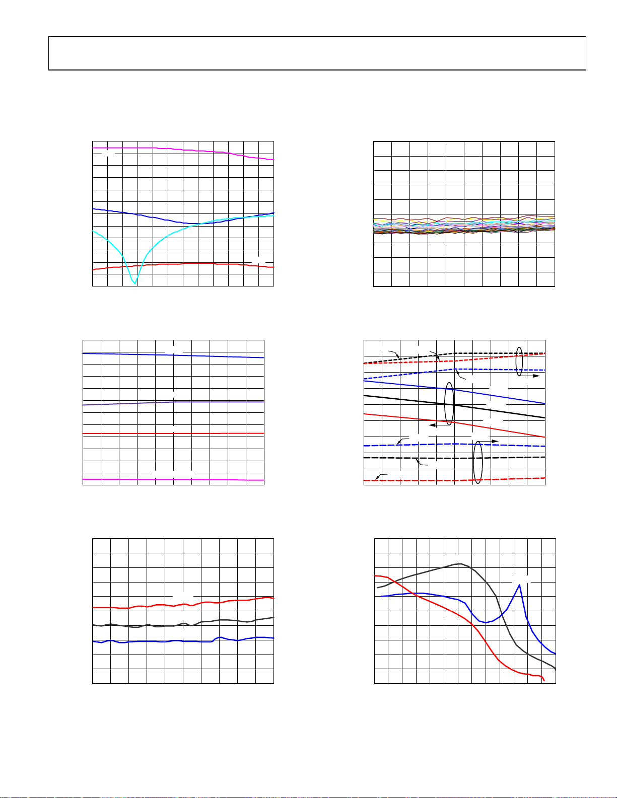
900 MHz, VPOS = 5 V
Matched for optimal noise figure, external matching circuit included.
25
S21
20
15
10
5
0
S11
–5
–10
–15
S-PARAMETERS ( dB)
–20
–25
–30
–35
600 650 700 750 800 850 900 950 1000 1050 1100 1150 1200
S22
FREQUENCY (MHz)
Figure 3. Typical S-Parameters, Log Magnitude
24
22
20
18
16
14
12
10
8
6
NOISE FI GURE AND GAIN (d B)
4
2
0
850 860 870 880 890 900 910 920 930 940 950
GAIN
OIP3
P1dB
NOISE FI GURE
FREQUENCY (MHz )
Figure 4. Noise Figure, Gain, OIP3, and P1dB vs. Frequency
2.0
1.8
1.6
1.4
1.2
1.0
0.8
NOISE FIGURE (dB)
0.6
0.4
0.2
0
800 820 840 860 880 900 920 940 960 980 1000
+85°C
+25°C
–40°C
FREQUENCY (MHz)
Figure 5. Noise Figure vs. Temperature
S12
06829-003
60
55
50
45
40
35
30
25
20
OIP3 AND P1dB (dBm)
15
10
5
0
06829-004
06829-005
2.0
1.8
1.6
1.4
1.2
1.0
0.8
NOISE FIGURE (dB)
0.6
0.4
0.2
0
800 820 840 860 880 900 920 940 960 980 1000
FREQUENCY (MHz)
Figure 6. Noise Figure vs. Frequency at 25°C, Multiple Devices
23.5
+25°C
23.0
22.5
22.0
21.5
21.0
GAIN (dB)
20.5
20.0
19.5
19.0
850 860 870 880 890 900 910 920 930 940 950
+85°C
+85°C
GAIN
–40°C
+25°C
FREQUENCY (MHz )
–40°C
–40°C
+25°C
+85°C
P1dB
Figure 7. Gain, OIP3, and P1dB vs. Temperature
40
38
36
34
32
30
28
OIP3 (dBm)
26
24
22
20
–4–20246810121416182022
Figure 8. OIP3 vs. Output Power (P
+25°C
+85°C
P
PER TONE (dBm)
OUT
) and Temperature
OUT
OIP3
–40°C
06829-006
36
34
32
30
28
26
24
OIP3 AND P1dB (dBm)
22
20
18
06829-008
06829-007
Rev. A | Page 7 of 24

ADL5523
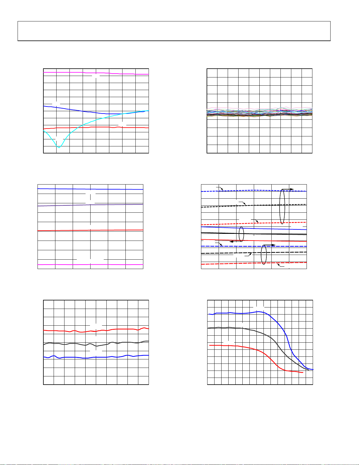
1950 MHZ, VPOS = 5 V
Matched for optimal noise figure, external matching circuit included.
20
15
10
5
0
S11
–5
–10
–15
–20
S-PARAMETERS ( dB)
–25
–30
–35
–40
S22
1800 1850 1900 1950 2000 2050 2100 2150 2200
S21
FREQUENCY (MHz)
Figure 9. Typical S-Parameters, Log Magnitude
18
16
14
12
10
8
6
4
NOISE FI GURE AND GAIN (d B)
2
0
1920 1930 1940 1950 1960 1970 1980
GAIN
OIP3
P1dB
NOISE FI GURE
FREQUENCY (MHz )
Figure 10. Noise Figure, Gain, OIP3, and P1dB vs. Frequency
2.0
1.8
1.6
1.4
1.2
1.0
0.8
NOISE FI G URE (dB)
0.6
0.4
0.2
0
1800 1820 1840 1860 1880 1900 1920 1940 1960 1980 2000
+85°C
+25°C
–40°C
FREQUENCY (MHz)
Figure 11. Noise Figure vs. Temperature
S12
06829-009
45
40
35
30
25
20
15
OIP3 AND P1dB (dBm)
10
5
0
06829-010
06829-011
2.0
1.8
1.6
1.4
1.2
1.0
0.8
NOISE FI G URE (dB)
0.6
0.4
0.2
0
1800 1820 1840 1860 1880 1900 1920 1940 1960 1980 2000
FREQUENCY (MHz)
Figure 12. Noise Figure vs. Frequency at 25°C, Multiple Devices
20.5
–40°C
20.0
19.5
19.0
18.5
18.0
17.5
17.0
GAIN (dB)
16.5
–40°C
16.0
15.5
15.0
14.5
1920 1930 1940 1950 1960 1970 1980
+25°C
+85°C
GAIN
+25°C
FREQUENCY (MHz )
+25°C
+85°C
P1dB
OIP3
+85°C
Figure 13. Gain, OIP3, and P1dB vs. Temperature
42
40
38
36
34
32
30
28
OIP3 (dBm)
26
24
22
20
18
–8 –6 –4 0–2 246810121416182022
+85°C
Figure 14. OIP3 vs. Output Power (P
+25°C
P
PER TONE (dBm)
OUT
–40°C
) and Temperature
OUT
–40°C
06829-012
40
38
36
34
32
30
28
26
24
OIP3 AND P1dB (dBm)
22
20
18
16
06829-013
06829-014
Rev. A | Page 8 of 24
 Loading...