

Page 1
DC to 6 GHz
V
Data Sheet
FEATURES
Envelope tracking RF detector with output proportional to
input voltage
Separate TruPwr rms output
No balun or external tuning required
Excellent temperature stability
Input power dynamic range of 47 dB
Input frequency range from dc to 6 GHz
130 MHz envelope bandwidth
Envelope delay: 2 ns
Single-supply operation: 4.75 V to 5.25 V
Supply current: 21.5 mA
Power-down mode: 130 μW
APPLICATIONS
RMS power and envelope detection of W-CDMA, CDMA2000,
LTE, and other complex waveforms
Drain modulation based power amplifier linearization
Power amplifier linearization employing envelope-tracking
methods
Envelope and TruPwr RMS Detector
ADL5511
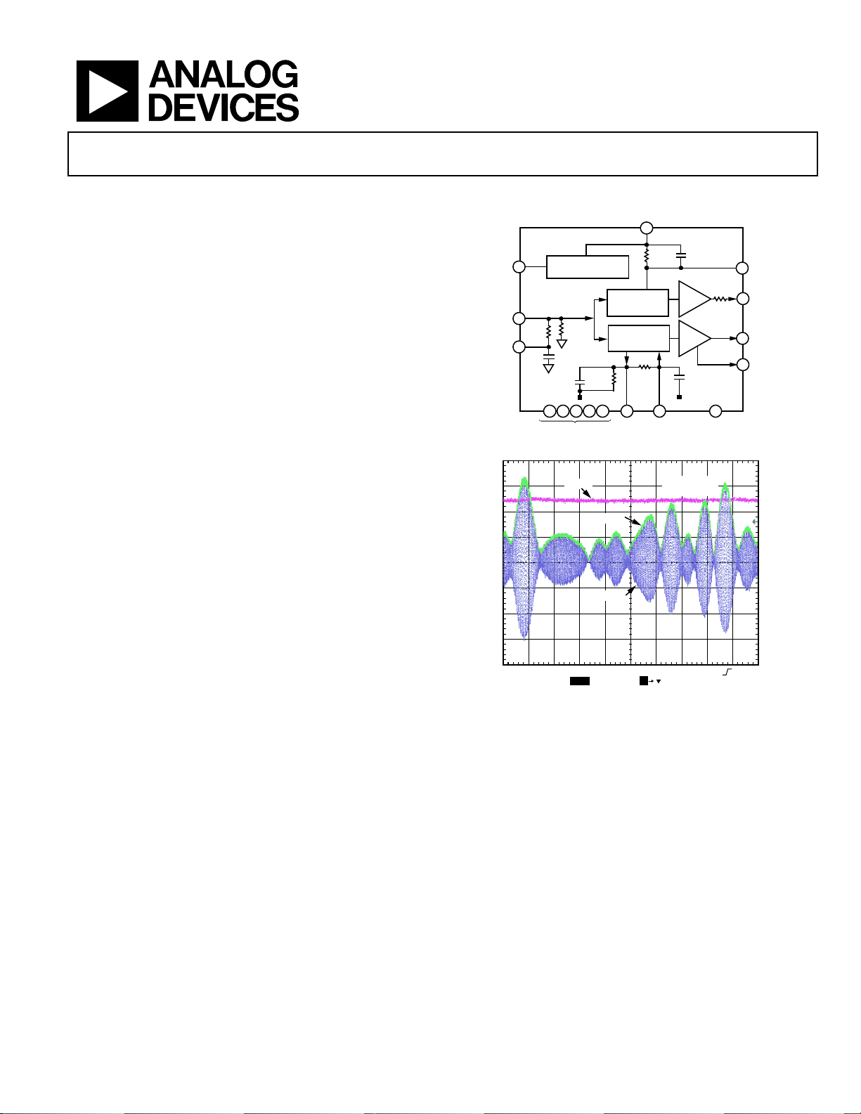
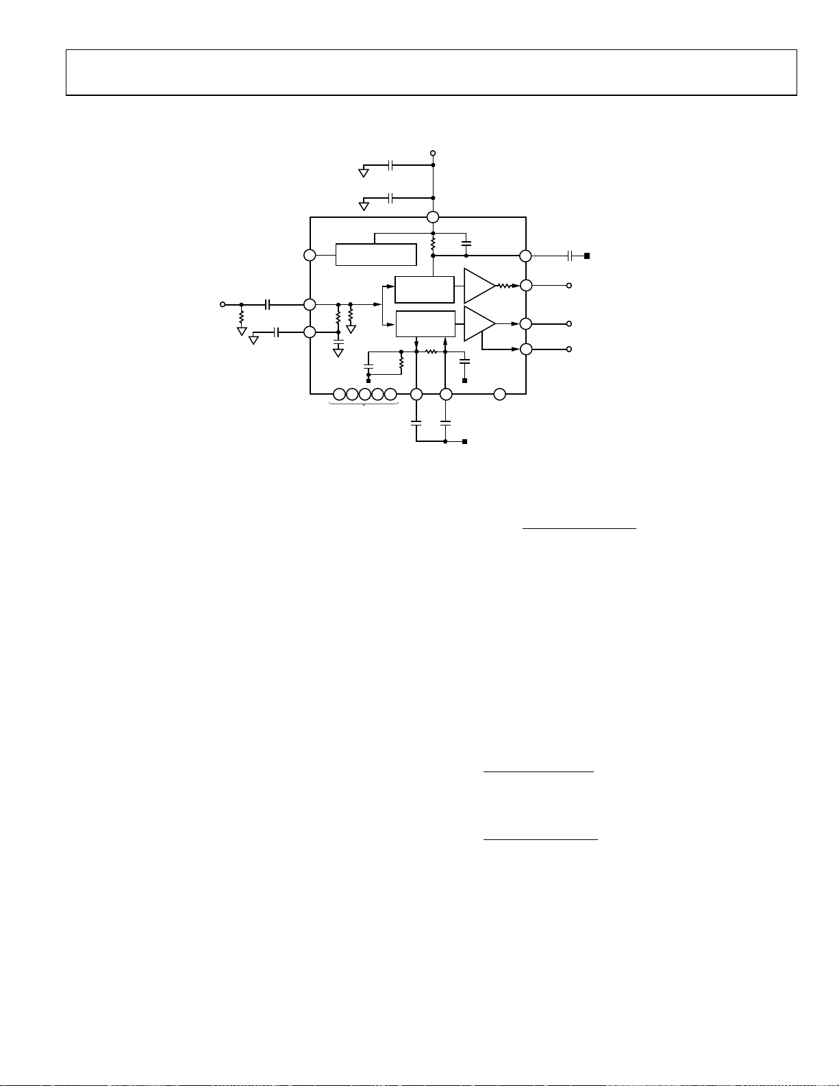
FUNCTIONAL BLOCK DIAGRAM
POS
15
400Ω
RMS
ENVELOPE
250Ω
FLT2
FLT3
Figure 1.
20pF
G = 1.7
G = 1.5
0.8pF
CH1 HIGH
20mV
100Ω
COMM
14
11
10
9
FLT4
VRMS
VENV
EREF
09602-001
ENBL
RFIN
FLT1
ADL5511
BIAS AND POWER-
4
DOWN CONTROL
2
10kΩ
3
250Ω
5pF
400Ω
0.4pF
VPOS VPOS
13 6 7 8 12 16 1 5
NC
VRMS
VENV
GENERAL DESCRIPTION
The ADL5511 is an RF envelope and TruPwr™ rms detector.
The envelope output voltage is presented as a voltage that is
proportional to the envelope of the input signal. The rms
output voltage is independent of the peak-to-average ratio
of the input signal.
The rms output is a linear-in-V/V voltage with a conversion
gain of 1.9 V/V rms at 900 MHz. The envelope output has a
conversion gain of 1.46 V/V at 900 MHz and is referenced to
an internal 1.1 V reference voltage, which is available on the
EREF pin.
RF INPUT
CH1 200mV Ω CH2 30.8mV Ω M 100ns A CH4 1.60V
CH3 200mV
CH4 234mV Ω
T –68ns
09602-002
Figure 2. RMS and Envelope Response to a 20 MHz QPSK-Based LTE Carrier
(Test Model E-TM1_1_20MHz)
The ADL5511 can operate from dc to 6 GHz on signals with
envelope bandwidths up to 130 MHz.
The extracted envelope can be used for RF power amplifier
(PA) linearization and efficiency enhancements and the rms
output can be used for rms power measurement. The high rms
accuracy and fast envelope response are particularly useful for
envelope detection and power measurement of broadband, high
peak-to-average signals that are used in CDMA2000, W-CDMA,
and LTE systems.
The ADL5511 operates from −40°C to +85°C and is available in
a 16-lead, 3 mm × 3 mm LFCSP package.
Rev. A
Information furnished by Analog Devices is believed to be accurate and reliable. However, no
responsibility is assumed by Analog Devices for its use, nor for any infringements of patents or other
rights of third parties that may result from its use. Specifications subject to change without notice. No
license is granted by implication or otherwise under any patent or patent rights of Analog Devices.
Trademarks and registered trademarks are the property of their respective owners.
One Technology Way, P.O. Box 9106, Norwood, MA 02062-9106, U.S.A.
Tel: 781.329.4700 www.analog.com
Fax: 781.461.3113 ©2011–2012 Analog Devices, Inc. All rights reserved.
Page 2

ADL5511 Data Sheet
TABLE OF CONTENTS
Features .............................................................................................. 1
Applications ....................................................................................... 1
Functional Block Diagram .............................................................. 1
General Description ......................................................................... 1
Revision History ............................................................................... 2
Specifications ..................................................................................... 3
Absolute Maximum Ratings ............................................................ 7
ESD Caution .................................................................................. 7
Pin Configuration and Function Descriptions ............................. 8
Typical Performance Characteristics ............................................. 9
Circuit Description ......................................................................... 17
Envelope Propagation Delay ..................................................... 17
RMS Circuit Description ........................................................... 17
RMS Filtering .............................................................................. 17
Output Drive Capability and Buffering ................................... 18
Applications Information .............................................................. 19
Basic Connections ...................................................................... 19
Operation Below 1 GHz/Envelope Filtering ........................... 19
Choosing a Value for the RMS Averaging Capacitor (C
Envelope Tracking Accuracy .................................................... 21
Time Domain Envelope Tracking Accuracy........................... 21
VRMS and VENV Output Offset ............................................. 22
Device Calibration and Error Calculation .............................. 22
Error vs. Frequency .................................................................... 23
Evaluation Board ........................................................................ 24
Outline Dimensions ....................................................................... 26
Ordering Guide .......................................................................... 26
FLT 4
).. 20
REVISION HISTORY
2/12—Rev. 0 to Rev. A
Changes to Equation 4 ................................................................... 19
Updated Outline Dimensions ....................................................... 26
7/11—Revision 0: Initial Version
Rev. A | Page 2 of 28
Page 3

Data Sheet ADL5511
FREQUENCY RANGE
Input RFIN
DC 6
GHz
Output Voltage
Intercept
−5 mV
Input Range (±1 dB Error)
CW input
46 dB
SPECIFICATIONS
TA = 25°C, V
and V
RMS
Table 1.
Parameter Conditions Min Typ Max Unit
= 5 V, C
POS
= 100 nF, 75 Ω shunt termination resistor to ground on (ac-coupled) RFIN, three-point calibration on V
FLT4
at +5 dBm, −15 dBm, and −26 dBm, unless otherwise noted.
ENV
ENVELOPE CONVERSION (100 MHz) Input RFIN to output (V
ENV
− V
)
EREF
Input Range (±1 dB Error) CW input 46 dB
Maximum Input Level
Minimum Input Level
Conversion Gain V
±1 dB error
±1 dB error
= (Gain × VIN) + Intercept 1.42 V/V rms
ENV
17 dBm
−29 dBm
Intercept −5 mV
High Power In PIN = +10 dBm, +707 mV rms 1.00 V
Low Power In PIN = −20 dBm, +22.4 mV rms 26 mV
RMS Conversion Input RFIN to output (V
)
RMS
Input Range (±1 dB Error) CW input 46 dB
Maximum Input Level
Minimum Input Level
Conversion Gain V
±1 dB error
±1 dB error
= (Gain × VIN) + Intercept 1.92 V/V rms
RMS
17 dBm
−29 dBm
Intercept 11 mV
Output Voltage
High Power In PIN = +10 dBm, +707 mV rms 1.38 V
Low Power In PIN = −20 dBm, +22.4 mV rms 53 mV
ENVELOPE CONVERSION (900 MHz) Input RFIN to output (V
ENV
− V
)
EREF
Input Range (±1 dB Error) CW input 46 dB
Maximum Input Level
Minimum Input Level
Conversion Gain V
±1 dB error
±1 dB error
= (Gain × VIN) + Intercept 1.46 V/V rms
ENV
17 dBm
−29 dBm
Output Voltage
High Power In PIN = +10 dBm, +707 mV rms 1.02 V
Low Power In PIN = −20 dBm, +22.4 mV rms 26 mV
RMS Conversion Input RFIN to output (V
Maximum Input Level
Minimum Input Level
Conversion Gain V
±1 dB error
±1 dB error
= (Gain × VIN) + Intercept 1.9 V/V rms
RMS
)
RMS
17 dBm
−29 dBm
Intercept 13 mV
Output Voltage
High Power In PIN = +10 dBm, +707 mV rms 1.35 V
Low Power In PIN = −20 dBm, +22.4 mV rms 54 mV
Rev. A | Page 3 of 28
Page 4

ADL5511 Data Sheet
Input Range (±1 dB Error)
CW Input
47 dB
Minimum Input Level
±
−30 dBm
Intercept
−5 mV
High Power In
PIN = +10 dBm, +707 mV rms
1.07 V
RMS Conversion
Input RFIN to output (V
)
Maximum Input Level
±
17 dBm
Conversion Gain
V
= (Gain × VIN) + Intercept
1.99 V/V rms
Output Voltage
Low Power In
PIN = −20 dBm, +22.4 mV rms
56 mV
Parameter Conditions Min Typ Max Unit
ENVELOPE CONVERSION (1900 MHz) Input RFIN to output (V
Input Range (±1 dB Error) CW input 47 dB
Maximum Input Level
Minimum Input Level
Conversion Gain V
±1 dB error
±1 dB error
= (Gain × VIN) + Intercept 1.5 V/V rms
ENV
Intercept −5 mV
Output Voltage
High Power In PIN = +10 dBm, +707 mV rms 1.05 V
Low Power In PIN = −20 dBm, +22.4 mV rms 28 mV
RMS Conversion Input RFIN to output (V
Input Range (±1 dB Error) CW input 47 dB
Maximum Input Level
Minimum Input Level
Conversion Gain V
±1 dB error
±1 dB error
= (Gain × VIN) + Intercept 1.96 V/V rms
RMS
Intercept 14 mV
Output Voltage
High Power In PIN = +10 dBm, +707 mV rms 1.40 V
Low Power In PIN = −20 dBm, +22.4 mV rms 56 mV
ENVELOPE CONVERSION (2140 MHz) Input RFIN to output (V
− V
ENV
)
EREF
17 dBm
−30 dBm
)
RMS
17 dBm
−30 dBm
− V
ENV
)
EREF
Maximum Input Level
±1 dB error
17 dBm
1 dB error
Conversion Gain V
= (Gain × VIN) + Intercept 1.53 V/V rms
ENV
Output Voltage
Low Power In PIN = −20 dBm, +22.4 mV rms 28 mV
RMS
Input Range (±1 dB Error) CW input 47 dB
1 dB error
Minimum Input Level
±1 dB error
RMS
−30 dBm
Intercept 13 mV
High Power In PIN = +10 dBm, +707 mV rms 1.42 V
Rev. A | Page 4 of 28
Page 5

Data Sheet ADL5511
Low Power In
PIN = −20 dBm, +22.4 mV rms
57 mV
Parameter Conditions Min Typ Max Unit
ENVELOPE CONVERSION (2600 MHz) Input RFIN to output (V
Input Range (±1 dB Error) CW Input 47 dB
Maximum Input Level
Minimum Input Level
Conversion Gain V
±1 dB error
±1 dB error
= (Gain × VIN) + Intercept 1.56 V/V rms
ENV
Intercept −3 mV
Output Voltage
High Power In PIN = +10 dBm, +707 mV rms 1.10 V
Low Power In PIN = −20 dBm, +22.4 mV rms 30 mV
RMS Conversion Input RFIN to output (V
Input Range (±1 dB Error) CW input 47 dB
Maximum Input Level
Minimum Input Level
Conversion Gain V
±1 dB error
±1 dB error
= (Gain × VIN) + Intercept 2.04 V/V rms
RMS
Intercept 15 mV
Output Voltage
High Power In PIN = +10 dBm, +707 mV rms 1.46 V
Low Power In PIN = −20 dBm, +22.4 mV rms 58 mV
ENVELOPE CONVERSION (3500 MHz) Input RFIN to output (V
Input Range (±1 dB Error) CW Input 47 dB
Maximum Input Level
Minimum Input Level
Conversion Gain V
±1 dB error
±1 dB error
= (Gain × VIN) + Intercept 1.56 V/V rms
ENV
Intercept −5 mV
Output Voltage
High Power In PIN = +10 dBm, +707 mV rms 1.10 V
Low Power In PIN = −20 dBm, +22.4 mV rms 28 mV
RMS Conversion Input RFIN to output (V
Input Range (±1 dB Error) CW input 47 dB
Maximum Input Level
Minimum Input Level
Conversion Gain V
±1 dB error
±1 dB error
= (Gain × VIN) + Intercept 2.03 V/V rms
RMS
Intercept 12 mV
Output Voltage
High Power In PIN = +10 dBm, +707 mV rms 1.46 V
− V
ENV
)
EREF
17 dBm
−30 dBm
)
RMS
17 dBm
−30 dBm
− V
ENV
)
EREF
17 dBm
−30 dBm
)
RMS
17 dBm
−30 dBm
Rev. A | Page 5 of 28
Page 6

ADL5511 Data Sheet
Envelope Bandwidth
3 dB 130 MHz
Logic Level to Disable Power
4.75 V ≤ V
≤ 5.25 V
2.0
V
Parameter Conditions Min Typ Max Unit
ENVELOPE CONVERSION (6000 MHz) Input RFIN to output (V
Input Range (±1 dB Error) CW Input 45 dB
Maximum Input Level
Minimum Input Level
Conversion Gain V
±1 dB error
±1 dB error
= (Gain × VIN) + Intercept 0.85 V/V rms
ENV
Intercept −10 mV
Output Voltage
High Power In PIN = +10 dBm, +707 mV rms 0.60 V
Low Power In PIN = −20 dBm, +22.4 mV rms 11 mV
RMS Conversion Input RFIN to output (V
Input Range (±1 dB Error) CW input 45 dB
Maximum Input Level
Minimum Input Level
Conversion Gain V
±1 dB error
±1 dB error
= (Gain × VIN) + Intercept 1.11 V/V rms
RMS
Intercept 7 mV
Output Voltage
High Power In PIN = +10 dBm, +707 mV rms 0.80 V
Low Power In PIN = −20 dBm, +22.4 mV rms 35 mV
ENVELOPE OUTPUT Pin VENV
Maximum Output Voltage V
= 5 V, R
POS
≥ 500 Ω, C
LOAD
Output Offset No signal at RFIN 2 mV
− V
ENV
)
EREF
17 dBm
−28 dBm
)
RMS
17 dBm
−28 dBm
≤ 10 pF 3.5 V
LOAD
Pulse Response Time Input level = no signal to 5 dBm, 10% to
90% response time
4 ns
Envelope Delay RFIN to VENV 2 ns
Output Current Drive Load = 500 Ω||10 pF 15 mA
RMS OUTPUT Pin VRMS
Maximum Output Voltage V
= 5 V, R
POS
≥ 10 kΩ 3.8 V
LOAD
Output Offset No signal at RFIN 23 mV
Output Current Drive Load = 1.3 kΩ 3 mA
ENABLE INTERFACE Pin ENBL
Logic Level to Enable Power 4.75 V ≤ V
≤ 5.25 V 3.6 V
POS
POS
POWER SUPPLIES
Operating Range −40°C < TA < +85°C 4.75 5.25 V
Quiescent Current RFIN < −10 dBm, ENBL high 21.5 mA
RFIN < −10 dBm, ENBL low 26 μA
RFIN = 15 dBm, ENBL high 43.8 mA
Rev. A | Page 6 of 28
Page 7
Data Sheet ADL5511
θJA
68.9°C/W
θJC
17.5°C/W
ABSOLUTE MAXIMUM RATINGS
Table 2.
Parameter Rating
Supply Voltage, VPOS 5.5 V
ENBL 0 V, VPOS
RFIN (RFIN AC-Coupled) 5.6 V p-p
Equivalent RF Power (Peak Envelope Power or
CW), re: 50 Ω
Internal Power Dissipation 580 mW
19 dBm
Stresses above those listed under Absolute Maximum Ratings
may cause permanent damage to the device. This is a stress
rating only; functional operation of the device at these or any
other conditions above those indicated in the operational
section of this specification is not implied. Exposure to absolute
maximum rating conditions for extended periods may affect
device reliability.
Maximum Junction Temperature 125°C
Operating Temperature Range −40°C to +85°C
Storage Temperature Range −65°C to +150°C
ESD (FICDM) 1250 V
ESD (HBM) 2000 V
ESD CAUTION
Rev. A | Page 7 of 28
Page 8

ADL5511 Data Sheet
NOTES
1. NC = NO CONNECT. DO NOT CONNECT T O T HIS PIN.
2. THE EXPOSED PAD SHOULD BE CONNE
CTED
TO BOTH THERMAL AND
ELECTRICAL GROUNDS.
PIN 1
INDICATOR
1FLT3
2RFIN
3FLT1
4ENBL
11
VRMS
12 NC
10 VENV
9 EREF
5
6
NC
7
NC
8NC
15
16
14
13
TO
P VIEW
(Not to Scale)
ADL5511
COMM
FLT2
VPOS
FLT4
NC
09602-103
6, 7, 8, 12, 13
NC
Do not connect to these pins.
PIN CONFIGURATION AND FUNCTION DESCRIPTIONS
Figure 3. Pin Configuration
Table 3. Pin Function Descriptions
Pin No. Mnemonic Description
1, 16 FLT3, FLT2 External Envelope Filter. With the F LT 3 an d F LT 2 pins not connected, two internal low-pass filters (operating
in series) with corner frequencies of approximately 1000 MHz and 800 MHz remove the residual RF carrier (at
two times the original input frequency) from the envelope signal. External, supply-referenced capacitors
connected to FLT3 and FLT2 can be used to reduce this corner frequency. See the Basic Connections section
for more information.
2 RFIN RF Input. RFIN should be externally ac-coupled. RFIN has a nominal input impedance of 250 Ω. To achieve a
broadband 50 Ω input impedance, an external 75 Ω shunt resistor should be connected between the source
side of the ac coupling capacitor and ground.
3 F LT1 External Envelope Filter. A capacitor to ground on this pin can be used to reduce the nominal minimum
input frequency. The capacitance on this pin helps to reduce any residual RF carrier presence on the EREF
output pin. See the Basic Connections section for more information.
4 ENBL Device Enable/Disable. A logic high on this pin enables the device. A logic low on this pin disables the
device.
5 COMM Device Ground. Connect to a low impedance ground plane.
9 EREF Reference Voltage for Envelope Output. The nominal value is 1.1 V.
10 VENV Envelope Output. The voltage on this pin represents the envelope of the input signal and is referred to
EREF. VENV can source a current of up to 15 mA. Capacitive loading should not exceed 10 pF to achieve the
specified envelope bandwidth. Lighter loads should be chosen when possible. The nominal output voltages
on EREF and VENV with no signal present track with temperature. For dc-coupled envelope output, EREF
should be used as a reference giving the true envelope voltage of V
ENV
− V
. For ac coupling of the
EREF
envelope output, the VENV pin can drive a 50 Ω load, if maximum current drive capability of 15 mA is not
exceeded. See the Output Drive Capability and Buffering section for more information.
11 VRMS RMS Output Pin. This voltage is ground referenced and has a nominal swing of 0 V to 3.8 V. V
has a linear-
RMS
in-V/V transfer function with a nominal slope of 2 V/V.
14 F LT4 RMS Averaging Capacitor. Connect between FLT4 and VPOS.
15 VPOS Supply Voltage Pin. Operational range is 4.75 V to 5.25 V with a supply current of 21.5 mA.
0 EP Exposed Pad. The exposed pad should be connected to both thermal and electrical grounds.
Rev. A | Page 8 of 28
Page 9

Data Sheet ADL5511
0.001
0.01
0.1
1
10
–30 –25 –20 –15 –10 –5 0 5 10 15 20
OUTPUT (V)
INPUT (d Bm)
100MHz
900MHz
1900MHz
2140MHz
2600MHz
3500MHz
6000MHz
09602-003
0.001
0.01
0.1
1
10
–30 –25 –20 –15 –10 –5 0 5 10 15 20
OUTPUT (V)
INPUT (d Bm)
5V, –40°C
5V, +25°C
5V, +85°C
09602-004
0
5
10
15
20
25
30
35
40
45
50
55
60
65
70
75
–30 –25 –20 –15 –10 –5 0 5 10 15 20
SUPPLY CURRENT (mA)
INPUT (d Bm)
09602-005
–40°C
+25°C
+85°C
0.01
0.1
1
10
–30 –25 –20 –15 –10 –5 0 5 10 15 20
OUTPUT (V)
INPUT (d Bm)
100MHz
900MHz
1900MHz
2140MHz
2600MHz
3500MHz
6000MHz
09602-006
–30 –25 –20 –15 –10 –5 0 5 10 15 20
0.01
0.1
1
10
OUTPUT (V)
INPUT (d Bm)
5V, –40°C
5V, +25°C
5V, +85°C
09602-007
0
0.2
0.4
0.6
0.8
1.0
1.2
1.4
1.6
1.8
2.0
2.2
2.4
2.6
2.8
3.0
0
50
100
150
200
250
300
350
400
450
0 1 2 3 4 5 6
SHUNT CAPACIT ANCE ( pF)
SHUNT RESISTANCE (Ω)
FREQUENCY ( GHz)
09602-008
SHUNT CAPACIT ANCE
SHUNT RESIS TANCE
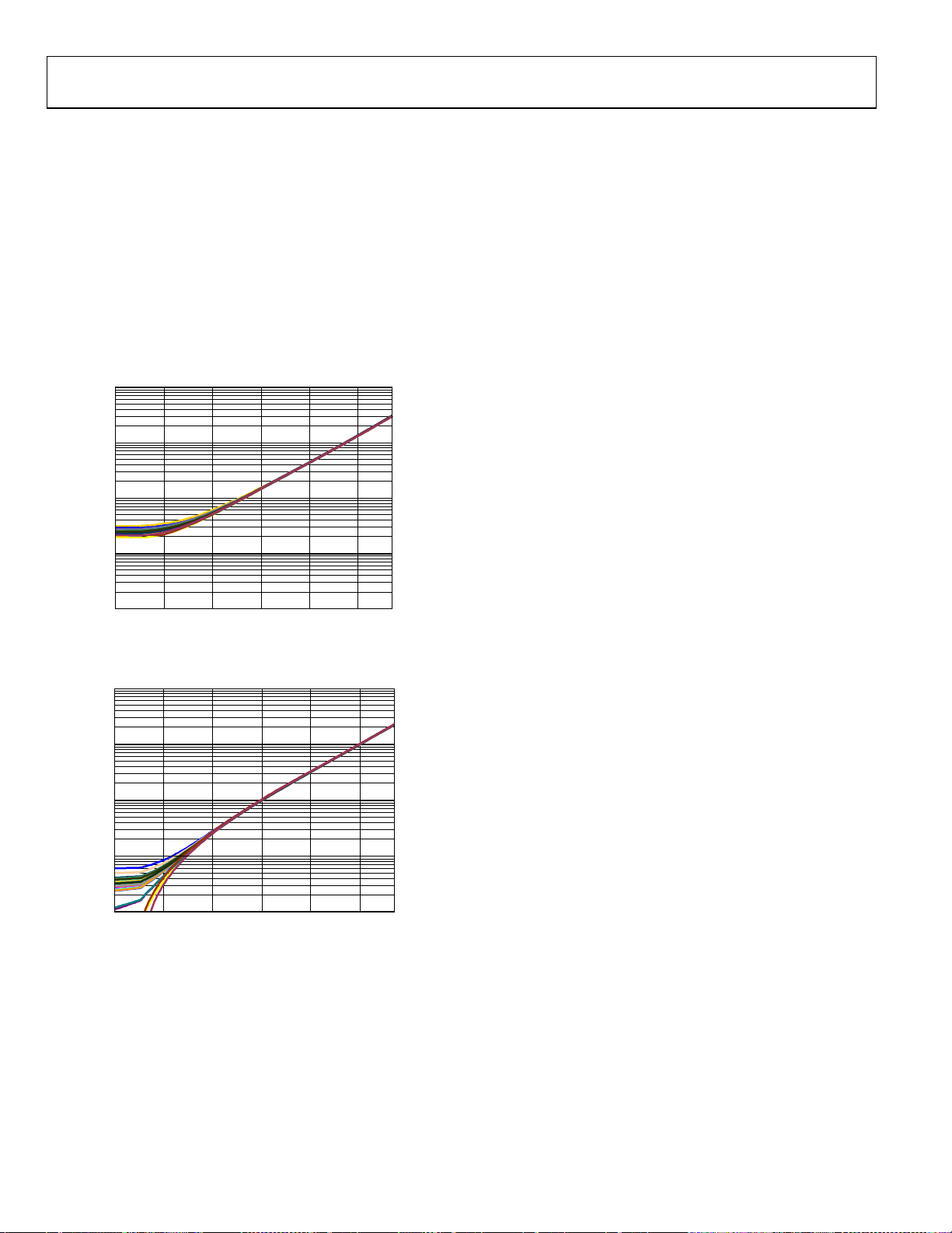
TYPICAL PERFORMANCE CHARACTERISTICS
TA = 25°C, V
+85°C (red), three-point calibration on V
= 5 V, C
POS
= 100 nF, 75 Ω shunt termination resistor to ground on (ac-coupled) RFIN, TA = +25°C (black), −40°C (blue),
FLT4
ENV
and V
at +5 dBm, −15 dBm, and −26 dBm, unless otherwise noted.
RMS
Figure 4. V
Figure 5. V
Output vs. Input Level, at Various Frequencies at 25°C,
ENV
Supply 5 V
Output vs. Input Level and Temperature at 1900 MHz,
ENV
Supply 5 V
Figure 7. V
Figure 8. V
Output vs. Input Level, at Various Frequencies at 25°C,
RMS
Supply 5 V
Output vs. Input Level and Temperature at 1900 MHz,
RMS
Supply 5 V
Figure 6. Supply Current vs. Input Level and Temperature
Figure 9. Input Impedance vs. Frequency
Rev. A | Page 9 of 28
Page 10

ADL5511 Data Sheet
–30 –25 –20 –15 –10 –5 0 5 10 15
–3
–2
–1
0
2
1
3
P
IN
(dBm)
ERROR (dB)
09602-009
–30 –25 –20 –15 –10 –5 0 5 10 15
–3
–2
–1
0
2
1
3
PIN (dBm)
ERROR (dB)
09602-010
–30 –25 –20 –15 –10 –5 0 5 10 15
–3
–2
–1
0
2
1
3
P
IN
(dBm)
ERROR (dB)
09602-011
–30 –25 –20 –15 –10 –5 0 5 10 15
–3
–2
–1
0
2
1
3
P
IN
(dBm)
ERROR (dB)
09602-012
–30 –25 –20 –15 –10 –5 0 5 10 15
–3
–2
–1
0
2
1
3
PIN (dBm)
ERROR (dB)
09602-013
–3
–2
–1
0
1
2
3
–30 –25 –20 –15 –10 –5 0 5 10 15
PIN (dBm)
ERROR (dB)
09602-014
Figure 10. V
Output Temperature Drift from +25°C, Three-Point
ENV
Calibration for Multiple Devices at −40°C, +25°C, and +85°C at 100 MHz
Figure 11. V
Output Temperature Drift from +25°C, Three-Point
RMS
Calibration for Multiple Devices at −40°C, +25°C, and +85°C at 100 MHz
Figure 13. V
Output Delta from +25°C Output Voltage for
ENV
Multiple Devices at −40°C and +85°C at 100 MHz
Figure 14. V
Output Delta from +25°C Output Voltage for
RMS
Multiple Devices at −40°C and +85°C at 100 MHz
Figure 12. V
Calibration for Multiple Devices at −40°C, +25°C, and +85°C at 900 MHz
Output Temperature Drift from +25°C, Three-Point
ENV
Figure 15. V
Output Delta from +25°C Output Voltage for
ENV
Multiple Devices at −40°C and +85°C at 900 MHz
Rev. A | Page 10 of 28
Page 11

Data Sheet ADL5511
–30 –25 –20 –15 –10 –5 0 5 10 15
–3
–2
–1
0
2
1
3
P
IN
(dBm)
ERROR (dB)
09602-015
–30 –25 –20 –15 –10 –5 0 5 10 15
–3
–2
–1
0
2
1
3
P
IN
(dBm)
ERROR (dB)
09602-029
–30 –25 –20 –15 –10 –5 0 5 10 15
–3
–2
–1
0
2
1
3
PIN (dBm)
ERROR (dB)
09602-030
–30 –25 –20 –15 –10 –5 0 5 10 15
–3
–2
–1
0
2
1
3
PIN (dBm)
ERROR (dB)
09602-031
–30 –25 –20 –15 –10 –5 0 5 10 15
–3
–2
–1
0
2
1
3
PIN (dBm)
ERROR (dB)
09602-032
–30 –25 –20 –15 –10 –5 0 5 10 15
–3
–2
–1
0
2
1
3
PIN (dBm)
ERROR (dB)
09602-033
Figure 16. V
Output Temperature Drift from +25°C, Three-Point
RMS
Calibration for Multiple Devices at −40°C, +25°C, and +85°C at 900 MHz
Figure 17. V
Output Temperature Drift from +25°C, Three-Point
ENV
Calibration for Multiple Devices at −40°C, +25°C, and +85°C at 1900 MHz
Figure 19. V
Output Delta from +25°C Output Voltage for
RMS
Multiple Devices at −40°C and +85°C at 900 MHz
Figure 20. V
Output Delta from +25°C Output Voltage for
ENV
Multiple Devices at −40°C and +85°C at 1900 MHz
Figure 18. V
Output Temperature Drift from +25°C, Three-Point
RMS
Calibration for Multiple Devices at −40°C, +25°C, and +85°C at 1900 MHz
Figure 21. V
Output Delta from +25°C Output Voltage for
RMS
Multiple Devices at −40°C and +85°C at 1900 MHz
Rev. A | Page 11 of 28
Page 12
ADL5511 Data Sheet
–30 –25 –20 –15 –10 –5 0 5 10 15
–3
–2
–1
0
2
1
3
P
IN
(dBm)
ERROR (dB)
09602-034
–30 –25 –20 –15 –10 –5 0 5 10 15
–3
–2
–1
0
2
1
3
PIN (dBm)
ERROR (dB)
09602-035
–30 –25 –20 –15 –10 –5 0 5 10 15
–3
–2
–1
0
2
1
3
PIN (dBm)
ERROR (dB)
09602-036
–30 –25 –20 –15 –10 –5 0 5 10 15
–3
–2
–1
0
2
1
3
P
IN
(dBm)
ERROR (dB)
09602-037
–30 –25 –20 –15 –10 –5 0 5 10 15
–3
–2
–1
0
2
1
3
PIN (dBm)
ERROR (dB)
09602-038
–30 –25 –20 –15 –10 –5 0 5 10 15
–3
–2
–1
0
2
1
3
PIN (dBm)
ERROR (dB)
09602-039
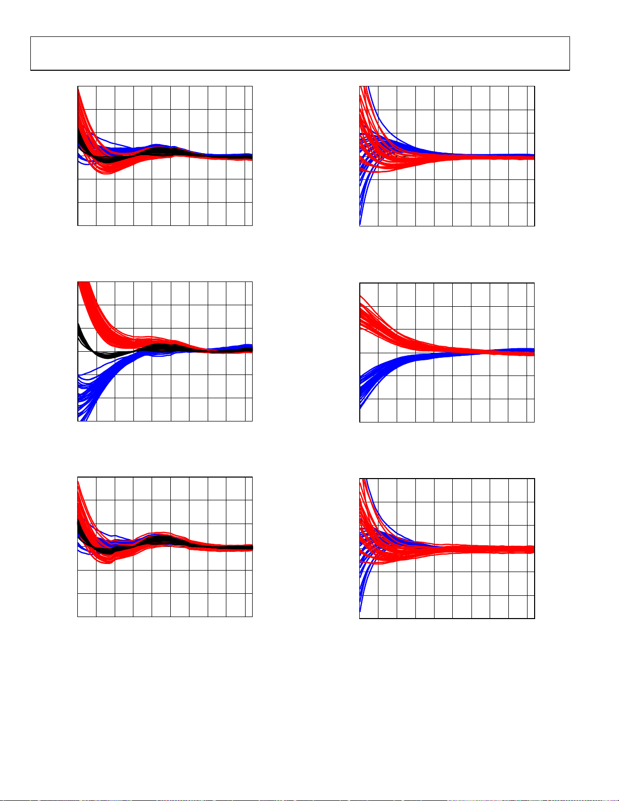
Figure 22. V
Output Temperature Drift from +25°C, Three-Point
ENV
Calibration for Multiple Devices at −40°C, +25°C, and +85°C at 2140 MHz
Figure 23. V
Output Temperature Drift from +25°C, Three-Point
RMS
Calibration for Multiple Devices at −40°C, +25°C, and +85°C at 2140 MHz
Figure 25. V
Output Delta from +25°C Output Voltage for
ENV
Multiple Devices at −40°C and +85°C at 2140 MHz
Figure 26. V
Output Delta from +25°C Output Voltage for
RMS
Multiple Devices at −40°C and +85°C at 2140 MHz
Figure 24. V
Output Temperature Drift from +25°C, Three-Point
ENV
Calibration for Multiple Devices at −40°C, +25°C, and +85°C at 2600 MHz
Figure 27. V
Output Delta from +25°C Output Voltage for
ENV
Multiple Devices at −40°C and +85°C at 2600 MHz
Rev. A | Page 12 of 28
Page 13
Data Sheet ADL5511
–30 –25 –20 –15 –10 –5 0 5 10 15
–3
–2
–1
0
2
1
3
PIN (dBm)
ERROR (dB)
09602-040
–30 –25 –20 –15 –10 –5 0 5 10 15
–3
–2
–1
0
2
1
3
PIN (dBm)
ERROR (dB)
09602-041
–3
–2
–1
0
2
1
3
PIN (dBm)
ERROR (dB)
09602-042
–30 –25 –20 –15 –10 –5 0 5 10 15
–3
–2
–1
0
2
1
3
P
IN
(dBm)
ERROR (dB)
09602-043
–30 –25 –20 –15 –10 –5 0 5 10 15
–3
–2
–1
0
2
1
3
P
IN
(dBm)
ERROR (dB)
09602-044
–30 –25
–20 –15 –10 –5 0 5 10 15
–3
–2
–1
0
2
1
3
PIN (dBm)
ERROR (dB)
09602-045
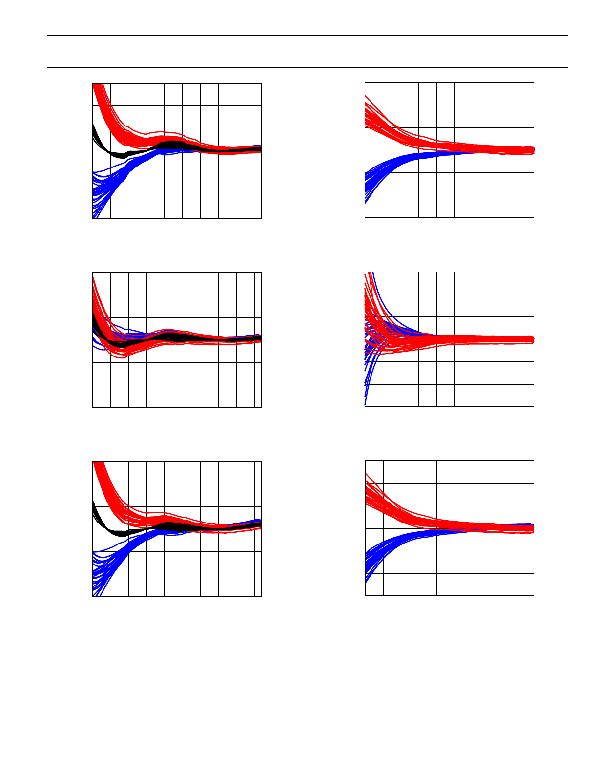
Figure 28. V
Output Temperature Drift from +25°C Linear Reference
RMS
for Multiple Devices at −40°C, +25°C, and +85°C, 2600 MHz Frequency
Figure 29. V
Output Temperature Drift from +25°C Linear Reference
ENV
for Multiple Devices at −40°C, +25°C, and +85°C, 3500 MHz Frequency
Figure 31. V
Output Delta from +25°C Output Voltage for
RMS
Multiple Devices at −40°C and +85°C at 2600 MHz
Figure 32. V
Output Delta from +25°C Output Voltage for
ENV
Multiple Devices at −40°C and +85°C at 3500 MHz
–30 –25 –20 –15 –10 –5 0 5 10 15
Figure 30. V
Output Temperature Drift from +25°C Linear Reference
RMS
for Multiple Devices at −40°C, +25°C, and +85°C, 3500 MHz Frequency
Figure 33. V
Output Delta from +25°C Output Voltage for
RMS
Multiple Devices at −40°C and +85°C at 3500 MHz
Rev. A | Page 13 of 28
Page 14

ADL5511 Data Sheet
–30 –25 –20 –15 –10 –5 0 5 10 15
–3
–2
–1
0
2
1
3
PIN (dBm)
ERROR (dB)
09602-046
–30 –25 –20 –15 –10 –5 0 5 10 15
–3
–2
–1
0
2
1
3
PIN (dBm)
ERROR (dB)
09602-047
–80
–70
–60
–50
–40
–30
–20
–10
0
10
20
–35 –30 –25 –20 –15 –10 –5 0 5 10 15
RFIN (dBm)
09602-020
THD (dBc)
CARRIER SUPPRES S ION (dBc)
ENVELOPE GAIN (dB)
–30 –25 –20 –15 –10 –5 0 5 10 15
–3
–2
–1
0
2
1
3
P
IN
(dBm)
ERROR (dB)
09602-016
–30 –25 –20 –15 –10 –5 0 5 10 15
–3
–2
–1
0
2
1
3
PIN (dBm)
ERROR (dB)
09602-017
–16
–14
–12
–10
–8
–6
–4
–2
0
2
1 10 100 1000
NORMALIZED V
ENV
FREQUENCY RESPONSE (dB)
ENVELOPE FREQUENCY (MHz)
–40°C
+25°C
+85°C
09602-065
Figure 34. V
Output Temperature Drift from +25°C Linear Reference
ENV
for Multiple Devices at −40°C, +25°C, and +85°C, 6000 MHz Frequency
Figure 35. V
Output Temperature Drift from +25°C Linear Reference
RMS
for Multiple Devices at −40°C, +25°C, and +85°C, 6000 MHz Frequency
Figure 37. V
Output Delta from +25°C Output Voltage for
ENV
Multiple Devices at −40°C and +85°C at 6000 MHz
Figure 38. V
Output Delta from +25°C Output Voltage for
RMS
Multiple Devices at −40°C and +85°C at 6000 MHz
Figure 36. THD on V
by a 20 MHz Sine Wave (Modulation Index = 0.25), V
vs. RF Input Level; 1900 MHz RF Input, AM Modulated
ENV
into a 50 Ω Spectrum Analyzer Load
Output AC-Coupled
ENV
Figure 39. Normalized V
Frequency Response, VENV AC-Coupled into a
ENV
50 Ω Spectrum Analyzer Load
Rev. A | Page 14 of 28
Page 15

Data Sheet ADL5511
CH1 200mV M10ns A CH2 1.88V
2
1
T 111.6ns
Ω
CH3 125mV
REF4 125mV 10ns
Ω
09602-023
PULSED RFIN
+5dBm
+1dBm
–3dBm
–10dBm
V
ENV
REF4 125mV 1µs
CH2 200mV M1µs A CH4 2.2V
R4
2
T –824ns
Ω
09602-024
+5dBm
PULSED RFIN
+1dBm
–3dBm
–10dBm
V
RMS
REF4 125mV 100µs
CH2 200mV M100µs A CH4 2.2V
R4
2
T –100.5µs
Ω
09602-025
+5dBm
+1dBm
–3dBm
–10dBm
V
RMS
PULSED RFIN
REF1 250mV 1µs
CH4 7V M1µs A CH4 3.78V
R1
4
T 3.996µs
09602-026
+5dBm
V
ENBL
+1dBm
–3dBm
–10dBm
V
ENV
REF1 220mV 1µs
CH4 7V M1µs A CH4 3.78V
R1
4
T 4.012µs
09602-027
+5dBm
+1dBm
–3dBm
–10dBm
V
ENBL
V
RMS
T 160.4µs
09602-028
+5dBm
+1dBm
–3dBm
–10dBm
V
ENBL
V
RMS
Figure 40. V
Figure 41. V
Output Response to Various RF Input Pulse Levels
ENV
900 MHz Frequency
Output Response to Various RF Input Pulse Levels
RMS
900 MHz Frequency, C
= Open
FLT4
Figure 43. V
Figure 44. V
4
Output Response to Enable Gating at Various RF Input Levels,
ENV
900 MHz Frequency
Output Response to Enable Gating at Various RF Input Levels,
RMS
900 MHz Frequency, C
= Open
FLT4
Figure 42. V
RMS
Output Response to Various RF Input Pulse Levels,
900 MHz Frequency, C
= 100 nF
FLT4
dBc
R4
CH4 7V M40µs A CH4 3.78V
900 MHz Frequency, C
= 100 nF
FLT4
Figure 45. V
REF4 220mV 40µs
Output Response to Enable Gating at Various RF Input Levels,
RMS
Rev. A | Page 15 of 28
Page 16

ADL5511 Data Sheet
–3
–2
–1
0
1
2
3
–25 –20 –15 –10 –5 0 5 10 15
ERROR (dB)
CW
QAM64
QPSK
1CWCDMA
4CWCDMA
LTE
INPUT (dBm )
09602-021
–3
–2
–1
0
1
2
3
–25 –20
–15 –10 –5 0 5 10 15
ERROR (dB)
INPUT (dBm )
CW
QAM64
QPSK
1CWCDMA
4CWCDMA
LTE
09602-022
Figure 46. V
RMS
Frequency = 900 MHz, C
4CW-CDMA, LTE Test Model E-TM1_1_20MHz)
Error from CW Linear Reference vs. Signal Modulation,
= 0.1 µF (CW, QPSK, QAM64, 1CW-CDMA,
LPF
Figure 47. V
Frequency = 2140 MHz, C
Error from CW Linear Reference vs. Signal Modulation,
RMS
= 0.1 µF (CW, QPSK, QAM64, 1CW-CDMA,
LPF
4CW-CDMA, LTE Test Model E-TM1_1_20MHz)
Rev. A | Page 16 of 28
Page 17

Data Sheet ADL5511
RFIN
ENBL
RMS
400Ω
20pF
ENVELOPE
VRMS
VENV
EREF
VPOS VPOS
VPOS
400Ω
FLT1
FLT2
FLT3
COMM
FLT4
0.8pF
0.4pF
10kΩ
5pF
250Ω
250Ω
100Ω
ADL5511
BIAS AND POW E R-
DOWN CONT ROL
G = 1.7
G = 1.5
NC
15
14
4
2
3
11
10
9
13 6 7 8 12 16
1 5
09602-049
T1T2
dtV
AVRMS
T2
T1
IN
−
×
×=
∫
2
pF20
)400π2(
1
−
Ω××
=
RMS
FLT4
f
C
CIRCUIT DESCRIPTION
The ADL5511 employs a proprietary rectification technique
to strip off the carrier of an input signal to reveal the true
envelope. In this first detection stage, the carrier frequency
is doubled and an on-chip two-pole passive low-pass filter
accurately preserves the envelope and filters out the carrier.
The poles of this filter, as defined by the on-chip RC filters
(0.4 pF, 400 Ω, 0.8 pF, 250 Ω) values allow some carrier
leakthrough for common RF frequencies. This is to ensure
that maximum envelope bandwidth can be maintained.
For more details, see the Basic Connections section.
Figure 48. Block Diagram
The extracted envelope is further processed in two parallel
channels, one computing the rms value of the envelope and
the other transferring the envelope with appropriate scaling
to the envelope output.
ENVELOPE PROPAGATION DELAY
The delay specified in this data sheet is with no external
capacitor at the FLT2 and FLT3 pins. The delay through the
ADL5511, although very small, depends upon a number of
factors, notable of which are internal filter component values
and op amp compensation capacitors. The delay will vary from
part to part by approximately ±15% due to process variations.
In addition, the choice of external FLT2 and FLT3 values, as
well as load on the VNEV pin will increase the delay. In this
case, the delay variation will be dominated by the part-to-part
tolerance of the external capacitors.
RMS CIRCUIT DESCRIPTION
The rms processing is done using a proprietary translinear
technique. This method is a mathematically accurate rms
computing approach and achieves unprecedented rms
accuracies for complex modulation signals irrespective of
the crest factor of the input signal. An integrating filter
capacitor does the square-domain averaging. The VRMS
output can be expressed as
(1)
Note that A is a scaling parameter that is decided on by the on-chip
resistor ratio, and there are no other scaling parameters involved in
this computation, which means that the rms output is inherently
free from any sources of error due to temperature, supply, and
process variation.
RMS FILTERING
The on-chip rms filtering corner is internally set by a 400 Ω resistor
and a 20 pF capacitor, yielding a corner frequency of approximately
20 MHz. Whereas this filters out all carrier frequencies, most of the
modulation envelope is not filtered. For adequate rms filtering,
connect an external filter capacitor between FLT4 (Pin 14) and
VPOS (Pin 15). This capacitance acts on the internal 400 Ω
resistor (see Figure 48) to yield a new corner frequency for the
rms filter given by
(2)
For example, a supply-referenced 0.1 µF capacitor on FLT4
reduces the corner frequency of the rms averaging circuit to
approximately 4 kHz.
RMS filtering has a direct impact on rms accuracy. For most
accurate detection, the rms filter corner should be low enough
to filter out most of the modulation content. This will correspond to a corner frequency that is significantly lower than the
bandwidth of the signal being measured. See the Choosing a
Value for the RMS Averaging Capacitor (C
details and filtering options.
) section for more
FLT4
Rev. A | Page 17 of 28
Page 18

ADL5511 Data Sheet
OUTPUT DRIVE CAPABILITY AND BUFFERING
The envelope output of the ADL5511 is presented on the VENV
pin as a single-ended buffered output with low output impedance. To achieve high envelope bandwidth, this output is not
ground referenced, unlike the VRMS output, which is ground
referenced.
The VENV output has a no signal dc value of about 1.1 V.
This dc reference is temperature dependent and is presented
as a standalone reference voltage on the EREF pin and as a
buffered output. The true envelope at any instant of time is
simply (V
differential output. EREF is a fixed dc voltage and V
all the envelope information.
The VENV output is capable of supporting a parallel load of
500 Ω and 10 pF at full-scale envelope output and maximum
bandwidth. Lighter loads (higher R and lower C) are always
recommended whenever possible to minimize power
consumption and achieve maximum possible bandwidth.
The maximum source/sink current capacity of the VNEV
output is 15 mA peak and load conditions should be such
that this is not exceeded. The maximum output voltage at
this pin is approximately (VPOS − 1.5) V.
For the case of ac coupling only, the VENV output can drive
a 50 Ω load, as long as the maximum signal swing does not
exceed an amplitude of approximately 1.5 V p-p. This corresponds to the peak signal current of 15 mA into the 50 Ω load.
If a 50 Ω drive capability is desired, the maximum input signal
to ADL5511 should be adjusted, such that this output swing
condition is not exceeded. A 50 Ω load should never be dc
coupled to the VENV output, as it presents a current draw of
>20 mA even for no-signal condition corresponding to 1.1 V
nominal dc voltage at the VENV pin.
ENV
− V
), but these two pins do not constitute a
EREF
ENV
carries
The VRMS buffered output can source a maximum current of
3 mA, but is not designed to sink any appreciable amount of
current. If current sink capability is desired at this pin, a shunt
resistance to ground can be connected. The VRMS output has
an on-chip series resistance of 100 Ω, to allow a low-pass
filtering of the residual ripple using a single shunt capacitor
at this pin. Large shunt capacitors at this pin may also require
a shunt resistor to be placed to allow fast discharging of the
capacitor. The internal shunt resistance on the VRMS pin is
10 kΩ. Note that any shunt resistance placed on this pin creates
a resistive divider with the on-chip 100 Ω series resistance.
The EREF output buffer also has 3 mA current sourcing
capability. The internal shunt resistance on this pin through
which any current must be sunk, is 12 kΩ. A capacitor to
ground can be placed on this pin to eliminate any RF or
envelope ripple at this pin to ensure that voltage at this pin
acts as a clean reference for the VENV output for all possible
carrier and envelope frequencies.
Viewing the Envelope on an Oscilloscope
When viewing the VENV output on an oscilloscope, use a low
capacitive FET probe. This reduces the capacitance presented to
the VENV output and avoids the corresponding effects of larger
capacitive loads.
Rev. A | Page 18 of 28
Page 19
Data Sheet ADL5511
RFIN
ENBL
RMS
400Ω
20pF
ENVELOPE
VRMS
RMS
OUTPUT
ENVELOPE
OUTPUT
ENVELOPE
REFERENCE
VENV
EREF
VPOS VPOS
VPOS
+5V
400Ω
FLT1
FLT2 FLT3
COMM
FLT4
VPOS
0.8pF
0.4pF
10kΩ
5pF
250Ω
250Ω
100Ω
ADL5511
BIAS AND POW E R-
DOWN CONT ROL
G = 1.7
G = 1.5
VPOS
NC
R5
75Ω
15
14
4
2
3
11
10
9
13 6 7
8 12 16 1 5
C14
0.1µF
C17
0.1µF
C13
100pF
C1
100pF
C2
100pF
C10
(SEE TEXT)
C6
(SEE TEXT)
09602-050
pF5
)000,10π2(
1
−
Ω××
=
3dB
FLT1
f
C
GHz1
)400pF4.0π2(
1
≅
Ω××
MHz800
)250pF8.0π2(
1
≅
Ω××
APPLICATIONS INFORMATION
BASIC CONNECTIONS
Basic connections for operation of the ADL5511 are shown in
Figure 49. The ADL5511 requires a single supply of 5 V. The
supply is connected to the VPOS supply pin. Decouple this
pin using two capacitors with values equal or similar to those
shown in Figure 49. Place these capacitors as close as possible
to the VPOS pin.
An external 75 Ω resistor combines with the relatively high
RF input impedance of the ADL5511 to provide a broadband
50 Ω match. Place an ac coupling capacitor between this resistor
and RFIN.
The envelope output is available on Pin 10 (VENV) and is
referenced to the 1.1 V dc voltage on Pin 9 (EREF).
The rms output voltage is available at the VRMS pin with rms
averaging provided by the supply-referenced capacitance on
Pin 14 (FLT4).
OPERATION BELOW 1 GHZ/ENVELOPE FILTERING
To operate the ADL5511 at frequencies below 1 GHz, a number
of external capacitors must be added to the FLT3, FLT2, and
FLT1 pins. These changes are in addition to the choice of an
appropriate rms averaging capacitor, see the Choosing a Value
for the RMS Averaging Capacitor (C
As part of the internal signal processing algorithm, the RF
input signal passes through a low-pass filter comprising of a
10 kΩ resistor and a 5 pF capacitor (see Figure 49). This
corresponds to a corner frequency of approximately 3.2 MHz.
If the carrier frequency is less than approximately ten times this
value (32 MHz), this corner frequency must be reduced. The
internal 5 pF capacitance can be augmented by connecting a
) section.
FLT4
Figure 49. Basic Connections
Rev. A | Page 19 of 28
ground referenced capacitor to Pin 3 (FLT1). The value of the
external capacitance is set using the following equation:
(3)
For example, a 100 pF capacitance on FLT1 will reduce the
corner frequency to 150 kHz. As a general guideline, this
corner frequency should be set to be at least one tenth of the
minimum expected carrier frequency. This ensures a flat
frequency response around the frequency of interest.
The envelope detection path of the ADL5511 includes internal
carrier-suppression low-pass filtering. With the FLT2 and FLT3
pins not connected, two internal 1 GHz and 800 MHz low-pass
filters (operating in series) remove the RF carrier from the
envelope output signal.
The equations for these filters are as follows:
(4)
and
(5)
Because the envelope detection circuitry includes a full-wave
rectifier, this filter has to primarily suppress the signal at twice
the original input frequency.
Page 20

ADL5511 Data Sheet
pF4.0
)400π2(
1
−
Ω××
=
FLT2
FLT2
f
C
pF8.0
)250π2(
1
−
Ω××
=
FLT3
FLT3
f
C
pF20
)400π2(
1
4
−
Ω××
=
FLT
FLT4
f
C
LTE Test Model E-TM1_1_10MHz
11.99 dB
10 MHz
100 nF
89 mV p-p
40 µs/140 µs
For input frequencies in the 900 MHz range, there will still be
significant carrier content on the envelope output. With the
two filters providing a combined 6 dB roll-off at approximately
900 MHz and with the residual carrier at 1.8 GHz, carrier
filtering of approximately 18 dB can be expected (the two
single-pole filters provide a combined roll-off of 12 dB per
octave.
The internal filtering of the carrier in the envelope detection
path can be augmented by adding additional supply-referenced
capacitance to the FLT2 and FLT3 pins. The required capacitance can be calculated using the following equations:
(6)
and
(7)
where f
For example, to set the corner frequency to 200 MHz, C
and C
and f
LT2
should be set to 1.6 pF and 2.4 pF, respectively.
FLT3
are the desired corner frequencies.
LT3
FLT2
The two corner frequencies should be set so that they are
approximately equal.
Care should be taken not to set the corner frequency of this
carrier suppression filter too low as it will start to degrade
envelope bandwidth. The ADL5511 has an envelope bandwidth
of 130 MHz. Thus, if the capacitors on FLT2 and FLT3 are so
big that the carrier-suppression corner frequency approaches
130 MHz, the carrier filtering effort will directly impact the
envelope bandwidth. Thus, the corner frequency should be set
low enough so that the RF carrier is adequately removed from
the envelope output while still maintaining the desired envelope
bandwidth. An alternative option would be to filter the carrier
at the VENV output using a higher order filter.
CHOOSING A VALUE FOR THE RMS AVERAGING
CAPACITOR (C
C
provides the averaging function for the internal rms
FLT4
computation, the result of which is available at the VRMS
output. As already noted, the on-chip rms filtering corner is
internally set by a 400 Ω resistor and a 20 pF capacitor, yielding a
corner frequency of approximately 20 MHz. For adequate rms
filtering, connect an external filter capacitor between FLT4
FLT4)
(Pin 14) and VPOS (Pin 15). This capacitance acts on the
internal 400 Ω resistor to yield a new corner frequency for the
rms filter given by the following equation:
(8)
For example, a supply-referenced 0.1 µF capacitor on FLT4
reduces the corner frequency of the rms averaging circuit to
approximately 4 kHz.
The size of the rms filtering capacitor has a direct impact on
the rms accuracy up to a point. For most accurate detection, the
rms filter corner should be low enough to filter out most of the
modulation content. This corresponds to a corner frequency
that is significantly less than the bandwidth of the signal being
measured.
Table 4 shows recommended minimum values of C
FLT4
for
popular modulation schemes. Using smaller capacitor values
than these will result in rms measurement errors; using higher
values will not further improve rms accuracy but will reduce the
output noise on VRMS at the expense of increased rise and fall
times. In Tab l e 4, rise and fall times are also shown along with
residual output noise.
The recommended minimum values for C
were experimen-
FLT4
tally determined by starting out with a large capacitance value
on the FLT4 pin (for example, 10 µF). The value of V
RMS
was
noted for a fixed input power level (for example, 0 dBm). The
value of C
with press-down capacitors) until the value of V
was then progressively reduced (this can be done
FLT4
started to
RMS
deviate from its original value (this indicates that the accuracy
of the rms computation is degrading and that C
is becoming
FLT4
too small).
The recommended minimum value for C
is roughly
FLT4
inversely proportional to the bandwidth of the input signal, that
is, wider bandwidth signals tend to require smaller minimum
filter capacitances. As already noted, the value of C
sets up
FLT4
an internal low pass corner frequency, which filters the rms
voltage. As carrier bandwidth increases, a larger proportion
of the residual noise (which has been effectively mixed down
to baseband) is filtered away. This results in smaller capacitances being required as carrier bandwidths increase.
Table 4. Recommended Minimum C
Modulation/Standard
W-CDMA, One-Carrier, TM1-64 9.83 dB 3.84 MHz 220 nF 98 mV p-p 82 µs/310 µs
W-CDMA Four-Carrier, TM1-64, TM1-32,
TM1-16, TM1-8
LTE Test Model E-TM1_1_4MHz 9.83 dB 4 MHz 220 nF 135 mV p-p 82 µs/310 µs
LTE Test Model E-TM1_1_20MHz 11.58 dB 20 MHz 47 nF 90 mV p-p 20 µs/70 µs
Values for Various Modulation Schemes (Pin = 0 dBm)
FLT4
PEP to RMS
Ratio
Signal
Bandwidth
C
FLT 4
(Min) Output Noise Rise/Fall Time (10% to 90%)
12.08 dB 18.84 MHz 100 nF 140 mV p-p 40 µs/140 µs
Rev. A | Page 20 of 28
Page 21

Data Sheet ADL5511
0.1
1
10
100
1000
10000
100000
1000000
10000000
0
100
200
300
400
500
600
700
800
1 10 100 1000
RISE/FALL TIME (µs)
C
FLT4
(nF)
OUTPUT NOISE (mV p-p)
OUTPUT NOISE (mV p-p)
10% TO 90% RISE TIME (µs)
90% TO 10% FAL L TIME (µs)
09602-066
–80
–70
–60
–50
–40
–30
–20
–10
0
10
20
–35 –30 –25 –20 –15 –10 –5 0 5 10 15
RFIN (dBm)
THD (dBc)
CARRIER SUPPRES S ION (dBc)
ENVELOPE GAIN (dB)
09602-069
For applications that are not response time critical, a
relatively large capacitor can be placed on the FLT4.
There is no maximum capacitance limit for C
FLT4
.
Figure 50 shows how output noise, rise time and fall time
vary vs. C
when the ADL5511 is driven by an 1.9 GHz
FLT4
LTE carrier with a bandwidth of 10 MHz (LTE Test Model
E-TM1_1_10MHz, peak-to-average ratio = 11.99 dB).
Figure 50. Output Noise, Rise and Fall Times vs. C
BW LTE Carrier (LTE Test Model E-TM1_1_10MHz) at 1.9 GHz with P
Capacitance, 10 MHz
FLT4
IN
= 0 dBm
ENVELOPE TRACKING ACCURACY
The envelope tracking accuracy of the ADL5511 is measured in
terms of the higher order distortion of the envelope output when
the RF input signal is AM modulated using a low-harmonic
sinusoid at a given frequency. Such an input sinusoidal envelope
has been generated using the ADL5390 multiplier modulator.
This generates a double sideband AM modulated signal of a
known modulation index. In this measurement, the ADL5511
acts as free-running AM demodulator without requiring a local
oscillator to demodulate the signal.
improves until it sharply degrades at an input power level of
approximately 13 dBm. This sharp decrease is caused by the
clipping of the AM signal’s peak envelope. Figure 51 also shows
carrier leakage at VENV in dBc with respect to the input carrier
amplitude.
This measurement, when conducted over the full input power
range of the ADL5511, suffers from measurement inaccuracies
of the input modulated signal due to the spectrum analyzer’s
noise floor and therefore does not accurately reveal the ADL5511’s
limitations at the lower end of the measurement range. In
addition to this, the process of generating an AM signal for this
test (using the ADL5390 multiplier) is not perfect and resulted
in a source signal whose envelope was not harmonically pure.
TIME DOMAIN ENVELOPE TRACKING ACCURACY
The envelope tracking accuracy of the ADL5511 can also be
assessed in the time domain by looking at the input peak power
levels that cause clipping.
The usable rms input power range of the ADL5511 varies
depending on the desired accuracy level and the peak-toaverage ratio of the input signal. Figure 4 shows the linear
operating range of the VENV output when the RF input is
driven by unmodulated sine waves at various frequencies.
This shows operation up to rms input levels of approximately
19 dBm. If the signal has a peak-to-average ratio that is greater
than the square root of two, the usable input range on RFIN
will decrease. In general, the maximum input power for linear
operation should be determined by the peak envelope power
(PEP) of the input signal. Figure 52 shows the time-domain
response of the VENV output to a 900 MHz LTE carrier with
a bandwidth of 20 MHz (Test Model E-TM1_2_20MHz).
The signal level of the carrier (7 dBm rms, 19 dBm PEP)
was deliberately increased until clipping was observed at
the VENV output.
Note that the peak envelope power of a signal is derived
based on the rms level of the signal during a peak cycle, that is
V p-p/√2. For example, a signal that achieves a peak voltage of
10 V (or 20 V p-p) has a PEP of 30 dBm. According to this
definition, the PEP of a sine wave is equal to its rms power
level because it has a constant envelope.
Figure 51. THD on V
by a 20 MHz Sine Wave (Modulation Index = 0.25), V
Figure 51 shows such a plot total harmonic distortion (THD)
of the VENV output vs. RF input power for the modulation
index of 0.25. As the input power level increases, the THD
vs. RF Input Level; 1900 MHz RF Input, AM Modulated
ENV
into a 50 Ω Spectrum Analyzer Load
Output AC-Coupled
ENV
09602-055
Figure 52. VENV Response to a 20 MHz LTE Carrier with a PEP of 19 dBm that
has been Triggered to Capture the Envelope’s Peak Level
Rev. A | Page 21 of 28
Page 22
ADL5511 Data Sheet
1
10
100
1000
10000
–40 –30 –20 –10 0 10
INPUT (d Bm)
V
RMS
(mV)
09602-067
1
10
100
1000
10000
–40 –30 –20 –10 0 10
INPUT (d Bm)
V
ENV
(mV)
09602-068
VRMS AND VENV OUTPUT OFFSET
The 900 MHz RF power sweeps in Figure 53 and Figure 54
show distributions of the VRMS and VENV outputs voltages
for multiple devices at 25°C. The VRMS output response
flattens out at approximately −30 dBm while the various VENV
response traces begin to fanout unpredictably (Figure 4 and
Figure 7 show this behavior at other frequencies). While these
plots suggest that operation at input levels down to −30 dBm is
feasible, account must also be taken for variations over
temperature. Figure 10 to Figure 38 show how the linearity
error starts to increase below input levels of −20 dBm (the
size of the error varies between VENV and VRMS and with
frequency).
Figure 53. VRMS Output vs. Input Level Distribution of 50 Devices,
900 MHz Frequency
DEVICE CALIBRATION AND ERROR CALCULATION
Because slope and intercept vary from device to device,
calibration must be performed to achieve high accuracy.
In general, calibration is performed by applying two or more
known input power levels to the ADL5511 and measuring
the corresponding output voltages. The calibration points
are generally chosen to be within the linear operating range
of the device. For a two-point calibration, the conversion gain
(or slope) and intercept are calculated for V
following equations:
Slope = (V
Intercept = V
OUT2
− V
OUT1
)/(V
OUT1
IN2
− (Slope × V
− V
IN1
where:
V
is the rms input voltage to RFIN.
IN
V
is the voltage output at VRMS or VENV.
OUT
Because the gain and intercept of the rms and envelope paths
will be different, both paths should be calibrated, that is, with a
measured signal applied to RFIN, V
ENV
that the voltage at VENV and VRMS is a steady-state value, a
constant envelope signal such as a sine wave should be used as
the source during calibration.
Once slope and intercept are calculated, an equation can be
written that allows calculation of the input rms or envelope level
using the following equations:
V
= (V
V
INRMS
INENV
= (V
− Intercept
RMS
− Intercept
ENV
VRMS
VENV
)/Slope
)/Slope
The law conformance error, that is, the difference between the
actual input level (V
level (V
), of these calculations can be calculated using
MEASURED
) and the measured/calculated input
IN_IDEAL
the following equation:
Error (dB) =
20 × log [(V
− Intercept)/(Slope × V
MEASURED
and V
RMS
) (9)
IN1
using the
ENV
) (10)
, and V
RMS
VENV
. To ensure
RMS
(11)
(12)
)] (13)
IN_IDEAL
Figure 54. VENV Output vs. Input Level Distribution of 50 Devices,
900 MHz Frequency
Rev. A | Page 22 of 28
Page 23

Data Sheet ADL5511
Figure 55 is a plot of this error for VENV at 1900 MHz for a
multiple devices at +25°C, +85°C, and −40°C with calibration
performed at two points, −14 dBm and +5 dBm (notice how
the error at 25°C at the calibration points is zero). These error
plots for all temperatures are calculated using the 25°C slope
and intercept. This is consistent with calibration in a mass
production environment where calibration at temperature is
generally not practical.
3
2
1
0
ERROR (d B)
–1
–2
–3
–30 –25 –20 –15 –10 –5 0 5 10 15
P
(dBm)
IN
Figu re 55. VENV Linear ity Error vs. Input Level and Temperature Using a
Two-Point Calibration at 1 900 MH z
–40°C
+25°C
+85°C
09602-058
By adding a third calibration point, the linearity of the
ADL5511 can be enhanced at lower power levels. With
a three-point calibration, calibration coefficients (slope and
intercept) are calculated for each segment (thus, there will
be two slopes and two intercepts).
Figure 56 shows the same data as Figure 55, but with a threepoint calibration (calibration points at −26 dBm, −15 dBm, and
+5 dBm. This helps to extend the usable operating range of the
ADL5511 well below −25 dBm.
3
2
1
0
ERROR (dB)
–1
–40°C
+25°C
+85°C
ERROR VS. FREQUENCY
Figure 57 and Figure 58 show how the V
voltages and error vary with input frequency when the
ADL5511 is calibrated at a single frequency. In this example,
the ADL5511 has been calibrated at 25°C at 1.9 GHz. The
plots also show how the output voltage and error vary above
and below this frequency.
600
500
400
300
OUTPUT (mV)
200
V
AT –40°C
RMS
AT +25°C
V
RMS
AT +85°C
V
100
RMS
ERROR AT –40°C
ERROR AT +2 5°C
ERROR AT +8 5°C
0
0 1000 2000 3000 4000 5000 6000
FREQUENCY (MHz)
Figure 57. VRMS Output vs. Frequency for a Fixed Input Power, P
Calibration at 1.9 GHz, 25°C
400
350
300
250
200
150
OUTPUT (mV)
100
V
AT –40°C
ENV
V
AT +25°C
ENV
V
AT +85°C
ENV
50
ERROR AT –40°C
ERROR AT +25°C
ERROR AT +85°C
0
0 1000 2000 3000 4000 5000 6000
FREQUENCY (MHz)
Figure 58. VENV Output vs. Frequency for a Fixed Input Power, P
Calibration at 1.9 GHz, 25°C
RMS
and V
ENV
output
6
4
2
0
–2
–4
–6
= 0 dBm,
IN
8
6
4
2
0
–2
–4
–6
–8
= 0 dBm,
IN
ERROR (dB)
09602-061
ERROR (dB)
09602-060
–2
–3
–30 –25
–20
–15 –10 –5 0 5 10 15
PIN (dBm)
Figu re 56. VENV L ineari ty Error vs. Input Level and Temperature Using a Three-
Point Calibration at 1 900 MH z
09602-059
Rev. A | Page 23 of 28
Page 24

ADL5511 Data Sheet
09602-062
EVALUATION BOARD
Figure 59 shows the schematic of the ADL5511 evaluation board.
This 4-layer board is powered by a single supply in the 4.75 V
to 5.25 V range. The power supply is decoupled by 100 pF and
0.1 µF capacitors.
Table 5 details the various configuration options of the evaluation
board. Figure 60 and Figure 61 show the bottom side and top
side layouts, respectively.
The RF input has a broadband match of 50 Ω using a single
75 Ω resistor at R5.
The VRMS output is accessible via a clip lead (a pad is also
available where an SMA connector is installed). The VENV
output is accessible via an SMA connector. For responsetime critical measurements where stray capacitance must
be minimized, R2 can be removed and a FET probe can be
attached to JP1 (JP1 must be installed).
Figure 59. Evaluation Board Schematic
Rev. A | Page 24 of 28
Page 25

Data Sheet ADL5511
09602-063
09602-064
C6, C10
Envelope carrier-removal filters (FLT2, FLT3). The corner frequency of the internal VENV two-pole
C6, C10 = open (Size 0402)
Figure 60. Layout of Evaluation Board, Bottom Side
Figure 61. Layout of Evaluation Board, Top Side
Table 5. Evaluation Board Configuration Options
Component Description Default Condition
VPOS, GND Ground and supply vector pins. Not applicable
C13, C14 Power supply decoupling. Nominal supply decoupling of 0.01 µF and 100 pF. C13 = 100 pF (Size 0402)
C14 = 0.1 µF (Size 0402)
C17 RMS filter capacitor (FLT4). The internal rms averaging capacitor can be augmented by
C17 = 0.1 µF (Size 0402)
placing additional capacitance in C17.
R5, C1 RF input interface. The 75 Ω resistor at R5 combines with the ADL5511 internal input
impedance to give a broadband input impedance of around 50 Ω. C1 is an ac coupling
R5 = 75 Ω (Size 0402)
C1 = 100 pF (Size 0402)
capacitor, which should be chosen according to nominal carrier frequency.
R18, C9 RMS output and output filtering. The combination of C9 and the internal 100 Ω output
resistance can be used to form a low-pass filter to reduce the output noise on the VRMS
output beyond the reduction due to C17 (capacitor on FLT4). The rms output is available
on the VRMS clip-on test point. To observe VRMS using an SMA cable, an SMA connector
can be soldered on to the pad labeled VRMS1.
R18 = 0 Ω (Size 0402)
C9 = open (Size 0402)
VRMS clip-on test point =
installed
VRMS1 SMA connector =
open
R19, C8, R2,
JP1
VENV output and output filtering. The VENV output is available on the VENV SMA
connector. If post-envelope filtering is desired, R19 and C8 can be used to form a low-pass
filter at the VENV output.
R2 can be removed to isolate the JP1 jumper from the VENV SMA connector and JP1 can
be installed and used to interface to a FET probe. This helps to eliminate any excessive
VENV SMA connector =
installed
R19, R2 = 0 Ω (Size 0402)
C8 = open (Size 0402)
JP1 = open
trace and connector capacitance.
R20, C7 Envelope reference output and output filtering. The EREF output is available on the EREF
clip-on test point. The dc reference voltage at Pin EREF can be filtered by the low-pass filter
formed by the combination of R20 and C7. To observe the EREF voltage using an SMA
cable, an SMA connector can be soldered onto the pad labeled EREF1.
R20 = 0 Ω (Size 0402)
C7 = open (Size 0402)
EREF clip-on test point =
installed
EREF1 SMA connector = open
R1, SW1 Device enable. When the switch is set toward the SW1 label, the ENBL pin is connected to VPOS,
which enables the ADL5511. In the opposite switch position, the ENBL pin is grounded which
R1 = 0 Ω (Size 0402)
SW1 = towards SW1 label
disables the ADL5511.
carrier-removal filter can be reduced by placing additional capacitors in C6 and C10.
C2 Envelope reference carrier-removal filter (FLT1). The internal filter that removes the carrier from
the envelope reference dc voltage can be augmented by placing a capacitor in C2.
R3, R14, R15,
R16, R17
Alternate interface. The P2 edge connector provides an alternate access point to the
various ADL5511 signals.
Rev. A | Page 25 of 28
C2 = 100 pF (Size 0402)
R3, R14, R15, R16, R17 = open
(Size 0402)
Page 26

ADL5511 Data Sheet
C
OUTLINE DIMENSIONS
PIN 1
ATOR
INDI
0.80
0.75
0.70
SEATING
PLANE
3.10
3.00 SQ
2.90
0.50
BSC
0.50
0.40
0.30
0.05 MAX
0.02 NOM
0.20 REF
0.30
0.23
0.18
13
12
9
8
BOTTOM VIEWTOP VIEW
COPLANARITY
0.08
N
1
I
P
C
I
A
N
I
16
EXPOSED
PAD
5
FOR PROP ER CONNECTI ON OF
THE EXPOSED PAD, REFER TO
THE PIN CONFIGURATION AND
FUNCTIO N DES CRI P TIONS
SECTION OF THIS DATA SHEET.
D
1
1.75
1.60 SQ
1.45
4
0.25 MIN
R
O
T
COMPLIANTTOJEDEC STANDARDS MO-220-WEE D- 6.
08-16-2010-E
Figure 62. 16-Lead Lead Frame Chip Scale Package [LFCSP_WQ]
3 mm × 3 mm Body, Very Thin Quad
(CP-16-22)
Dimensions shown in millimeters
ORDERING GUIDE
Model1 Temperature Range Package Description Package Option Ordering Quantity
ADL5511ACPZ-R7 −40°C to +85°C 16-Lead Lead Frame Chip Scale Package [LFCSP_WQ] CP-16-22 1500
ADL5511-EVALZ Evaluation Board
1
Z = RoHS Compliant Part.
Rev. A | Page 26 of 28
Page 27

Data Sheet ADL5511
NOTES
Rev. A | Page 27 of 28
Page 28

ADL5511 Data Sheet
©2011–2012 Analog Devices, Inc. All rights reserved. Trademarks and
NOTES
registered trademarks are the property of their respective owners.
D09602-0-2/12(A)
Rev. A | Page 28 of 28
 Loading...