

400 MHz to 6 GHz
Data Sheet
FEATURES
Output frequency range: 400 MHz to 6 GHz
1 dB output compression: ≥9.4 dBm from 450 MHz to 4 GHz
Output return loss ≤ 12 dB from 450 MHz to 4.5 GHz
Noise floor: −160 dBm/Hz @ 900 MHz
Sideband suppression: ≤−50 dBc @ 900 MHz
Carrier feedthrough: ≤−40 dBm @ 900 MHz
IQ3dB bandwidth: ≥ 750 MHz
Baseband input bias level
ADL5375-05: 500 mV
ADL5375-15: 1500 mV
Single supply: 4.75 V to 5.25 V
24-lead LFCSP_VQ package
APPLICATIONS
Cellular communication systems
GSM/EDGE, CDMA2000, W-CDMA, TD-SCDMA
WiMAX/LTE broadband wireless access systems
Satellite modems
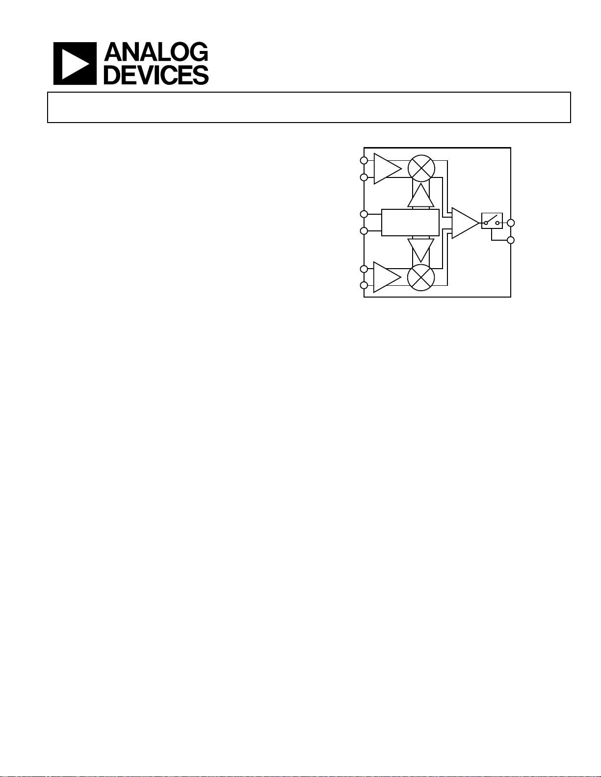
Broadband Quadrature Modulator
ADL5375
FUNCTIONAL BLOCK DIAGRAM
IBBP
IBBN
LOIP
LOIN
QBBN
QBBP
QUADRATURE
PHASE
SPLITTER
Figure 1.
ADL5375
RFOUT
DSOP
07052-001
GENERAL DESCRIPTION
The ADL5375 is a broadband quadrature modulator designed for
operation from 400 MHz to 6 GHz. Its excellent phase accuracy
and amplitude balance enable high performance intermediate
frequency or direct radio frequency modulation for communication systems.
The ADL5375 features a broad baseband bandwidth, along
with an output gain flatness that varies no more than 1 dB
from 450 MHz to 3.5 GHz. These features, coupled with a broadband output return loss of ≤−12 dB, make the ADL5375 ideally
suited for broadband zero IF or low IF-to-RF applications,
broadband digital predistortion transmitters, and multiband
radio designs.
The ADL5375 accepts two differential baseband inputs and
a single-ended LO. It generates a single-ended 50 Ω output.
The two versions offer input baseband bias levels of 500 mV
(ADL5375-05) and 1500 mV (ADL5375-15).
The ADL5375 is fabricated using an advanced silicon-germanium
bipolar process. It is available in a 24-lead, exposed paddle, leadfree, LFCSP_VQ package. Performance is specified over a −40°C
to +85°C temperature range. A lead-free evaluation board is
also available.
Rev. B
Information furnished by Analog Devices is believed to be accurate and reliable. However, no
responsibility is assumed by Analog Devices for its use, nor for any infringements of patents or other
rights of third parties that may result from its use. Specifications subject to change without notice. No
license is granted by implication or otherwise under any patent or patent rights of Analog Devices.
Trademarks and registered trademarks are the property of their respective owners.
One Technology Way, P.O. Box 9106, Norwood, MA 02062-9106, U.S.A.
Tel: 781.329.4700 www.analog.com
Fax: 781.461.3113 ©2007–2011 Analog Devices, Inc. All rights reserved.

ADL5375 Data Sheet
TABLE OF CONTENTS
Features .............................................................................................. 1
Applications ....................................................................................... 1
Functional Block Diagram .............................................................. 1
General Description ......................................................................... 1
Revision History ............................................................................... 2
Specifications ..................................................................................... 3
Absolute Maximum Ratings ............................................................ 7
ESD Caution .................................................................................. 7
Pin Configuration and Function Descriptions ............................. 8
Typical Performance Characteristics ............................................. 9
ADL5375-05 .................................................................................. 9
ADL5375-15 ................................................................................ 14
Theory of Operation ...................................................................... 19
Circuit Description..................................................................... 19
Basic Connections .......................................................................... 20
Power Supply and Grounding ................................................... 20
Baseband Inputs .......................................................................... 20
LO Input ...................................................................................... 20
RF Output .................................................................................... 20
Output Disable ............................................................................ 21
Applications Information .............................................................. 22
Carrier Feedthrough Nulling .................................................... 22
Sideband Suppression Optimization ....................................... 22
Interfacing the ADF4350 PLL to the ADL5375 ..................... 23
DAC Modulator Interfacing ..................................................... 24
GSM/EDGE Operation ............................................................. 27
W-CDMA Operation ................................................................. 28
LO Generation Using PLLs ....................................................... 29
Transmit DAC Options ............................................................. 29
Modulator/Demodulator Options ........................................... 29
Evaluation Board ............................................................................ 30
Characterization Setup .................................................................. 33
Outline Dimensions ....................................................................... 35
Ordering Guide .......................................................................... 35
REVISION HISTORY
9/11—Rev. A to Rev. B
Changes to Features Section............................................................ 1
Replaced Table 1 ............................................................................... 3
Changes to Typical Performance Characteristics Section ........... 9
Updated Output Disable Section .................................................. 21
Changes to Application Information Section ............................ 22
Changes to Evaluation Board Section .......................................... 30
Changes to Figure 80 ...................................................................... 34
Added Exposed Pad Notation to Outline Dimensions ............. 35
11/08—Rev. 0 to Rev. A
Change AD9779 to AD9779A .......................................... Universal
Added Endnote, I/Q Input Bias Level and Absolute
Voltage Level Parameters, Table 1 .................................................. 6
Added Absolute Voltage Level Parameter, Table 1 ....................... 6
12/07—Revision 0: Initial Version
Rev. B | Page 2 of 36

Data Sheet ADL5375
SPECIFICATIONS
VS = 5 V; TA = 25°C; LO = 0 dBm single-ended drive; baseband I/Q amplitude = 1 V p-p differential sine waves in quadrature with a
500 mV (ADL5375-05) or 1500 mV (ADL5375-15) dc bias; baseband I/Q frequency (f
Table 1.
Parameter Conditions
OPERATING FREQUENCY RANGE
Low frequency 400 400 MHz
High frequency 6000 6000 MHz
LO = 450 MHz
Output Power, P
V
OUT
= 1 V p-p differential 0.85 0.47 dBm
IQ
Modulator Voltage Gain RF output divided by baseband input voltage −3.1 −3.5 dB
Output P1dB 9.6 10 dBm
Output Return Loss −16.4 −15.2 dB
Carrier Feedthrough −47.5 -42.5 dBm
Sideband Suppression −37.6 −38 dBc
Quadrature Error 1.7 1.49 Degrees
I/Q Amplitude Balance 0.07 0.10 dB
Second Harmonic P
ADL5375-05 P
ADL5375-15 P
Third Harmonic P
ADL5375-05 P
ADL5375-15 P
Output IP2
− (fLO + (2 × fBB)) −75.9 −81.5 dBc
OUT
=0.85 dBm
OUT
= 0.47 dBm
OUT
− (fLO + (3 × fBB)) −51.5 −81.6 dBc
OUT
= 0.85 dBm
OUT
= 0.47 dBm
OUT
f1BB = 3.5 MHz, f2BB = 4.5 MHz, baseband I/Q
amplitude per tone = 0.5 V p-p differential
Output IP3
f1BB = 3.5 MHz, f2BB = 4.5 MHz, baseband I/Q
amplitude per tone = 0.5 V p-p differential
Noise Floor
I/Q inputs = 0 V differential with a dc bias
only, 20 MHz carrier offset
LO = 900 MHz
Output Power, P
V
OUT
= 1 V p-p differential 0.75 0.41 dBm
IQ
Modulator Voltage Gain RF output divided by baseband input voltage −3.2 −3.5 dB
Output P1dB 9.6 10 dBm
Output Return Loss −15.7 −14.7 dB
Carrier Feedthrough −45.1 −39.9 dBm
Sideband Suppression −52.8 −49.9 dBc
Quadrature Error 0.01 0.20 Degrees
I/Q Amplitude Balance 0.07 0.10 dB
Second Harmonic P
ADL5375-05 P
ADL5375-15 P
Third Harmonic P
ADL5375-05 P
ADL5375-15 P
Output IP2
− (fLO + (2 × fBB)) −75.8 −77.2 dBc
OUT
= 0.75 dBm
OUT
= 0.41 dBm
OUT
− (fLO + (3 × fBB)) −50.7 −72.7 dBc
OUT
= 0.75 dBm
OUT
= 0.41 dBm
OUT
f1BB = 3.5 MHz, f2BB = 4.5 MHz, baseband I/Q
amplitude per tone = 0.5 V p-p differential
Output IP3
f1BB = 3.5 MHz, f2BB = 4.5 MHz, baseband I/Q
amplitude per tone = 0.5 V p-p differential
Noise Floor
I/Q inputs = 0 V differential with a dc bias
only, 20 MHz carrier offset
) = 1 MHz, unless otherwise noted.
BB
ADL5375-05 ADL5375-15
Unit Min Typ Max Min Typ Max
65.4 64.7 dBm
26.6 23.6 dBm
−160.5 −157.0 dBm/Hz
62.6 64.5 dBm
25.9 23.4 dBm
−160.0 −157.1 dBm/Hz
Rev. B | Page 3 of 36

ADL5375 Data Sheet
ADL5375-05 ADL5375-15
Parameter Conditions
LO = 1900 MHz
Output Power, P
V
OUT
= 1 V p-p differential 0.53 0.49 dBm
IQ
Modulator Voltage Gain RF output divided by baseband input voltage −3.4 −3.4 dB
Output P1dB 9.9 10.5 dBm
Output Return Loss −16.2 −15.5 dB
Carrier Feedthrough −40.3 −35.5 dBm
Sideband Suppression −50.2 −49.4 dBc
Quadrature Error 0.02 0.21 Degrees
I/Q Amplitude Balance 0.07 0.10 dB
Second Harmonic P
ADL5375-05 P
ADL5375-15 P
Third Harmonic P
ADL5375-05 P
ADL5375-15 P
Output IP2
− (fLO + (2 × fBB)) −67.9 −72.1 dBc
OUT
= 0.53dBm
OUT
= 0.49dBm
OUT
− (fLO + (3 × fBB)) −51.8 −62.8 dBc
OUT
= 0.53dBm
OUT
= 0.49dBm
OUT
f1BB = 3.5 MHz, f2BB = 4.5 MHz, baseband I/Q
62.6 61 dBm
amplitude per tone = 0.5 V p-p differential
Output IP3
f1BB = 3.5 MHz, f2BB = 4.5 MHz, baseband I/Q
24.3 22.1 dBm
amplitude per tone = 0.5 V p-p differential
Noise Floor
I/Q inputs = 0 V differential with a dc bias
−160.0 −158.2 dBm/Hz
only, 20 MHz carrier offset
LO = 2150 MHz
Output Power, P
V
OUT
= 1 V p-p differential 0.73 0.57 dBm
IQ
Modulator Voltage Gain RF output divided by baseband input voltage −3.2 −3.4 dB
Output P1dB 10.0 10.6 dBm
Output Return Loss −17.1 −16.1 dB
Carrier Feedthrough −39.7 −34.2 dBm
Sideband Suppression −47.3 −50.2 dBc
Quadrature Error −0.16 −0.18 Degrees
I/Q Amplitude Balance 0.07 0.10 dB
Second Harmonic P
ADL5375-05 P
ADL5375-15 P
Third Harmonic P
ADL5375-05 P
ADL5375-15 P
Output IP2
− (fLO + (2 × fBB)) −71.3 −81.7 dBc
OUT
= 0.73 dBm
OUT
= 0.57 dBm
OUT
− (fLO + (3 × fBB)) −52.4 −65.3 dBc
OUT
= 0.73 dBm
OUT
= 0.57 dBm
OUT
f1BB = 3.5 MHz, f2BB = 4.5 MHz, baseband I/Q
61.6 61.8 dBm
amplitude per tone = 0.5 V p-p differential
Output IP3
f1BB = 3.5 MHz, f2BB = 4.5 MHz, baseband I/Q
24.2 22.3 dBm
amplitude per tone = 0.5 V p-p differential
Noise Floor
I/Q inputs = 0 V differential with a dc bias
−159.5 −157.9 dBm/Hz
only, 20 MHz carrier offset
LO = 2600 MHz
Output Power, P
V
OUT
= 1 V p-p differential 0.61 0.62 dBm
IQ
Modulator Voltage Gain RF output divided by baseband input voltage −3.4 −3.3 dB
Output P1dB 9.6 10.6 dBm
Output Return Loss −19.3 −18 dB
Carrier Feedthrough −36.5 −33.3 dBm
Sideband Suppression −48.3 −48.5 dBc
Quadrature Error −0.37 0.19 Degrees
I/Q Amplitude Balance 0.07 0.11 dB
Second Harmonic P
− (fLO + (2 × fBB)) −60.9 −55.9 dBc
OUT
Unit Min Typ Max Min Typ Max
Rev. B | Page 4 of 36

Data Sheet ADL5375
ADL5375-05 ADL5375-15
Parameter Conditions
ADL5375-05 P
ADL5375-15 P
Third Harmonic P
ADL5375-05 P
ADL5375-15 P
Output IP2
= 0.61 dBm
OUT
= 0.62 dBm
OUT
− (fLO + (3 × fBB)) −51.3 −57.6 dBc
OUT
= 0.61 dBm
OUT
= 0.62 dBm
OUT
f1BB = 3.5 MHz, f2BB = 4.5 MHz, baseband I/Q
55.0 50.1 dBm
amplitude per tone = 0.5 V p-p differential
Output IP3
f1BB = 3.5 MHz, f2BB = 4.5 MHz, baseband I/Q
22.7 20.7 dBm
amplitude per tone = 0.5 V p-p differential
Noise Floor
I/Q inputs = 0 V differential with a dc bias
−159.0 −157.6 dBm/Hz
only, 20 MHz carrier offset
LO = 3500 MHz
Output Power, P
V
OUT
= 1 V p-p differential 0.21 0.87 dBm
IQ
Modulator Voltage Gain RF output divided by baseband input voltage −3.8 −3.1 dB
Output P1dB 9.6 10.2 dBm
Output Return Loss −20.7 −19.4 dB
Carrier Feedthrough −30.4 −28.6 dBm
Sideband Suppression −48.3 −48.8 dBc
Quadrature Error 0.01 0.13 Degrees
I/Q Amplitude Balance 0.08 0.11 dB
Second Harmonic P
ADL5375-05 P
ADL5375-15 P
Third Harmonic P
ADL5375-05 P
ADL5375-15 P
Output IP2
− (fLO + (2 × fBB)) −55.8 −63 dBc
OUT
= 0.21 dBm
OUT
= 0.87 dBm
OUT
− (fLO + (3 × fBB)) −50.2 −56.2 dBc
OUT
= 0.21 dBm
OUT
= 0.87 dBm
OUT
f1BB = 3.5 MHz, f2BB = 4.5 MHz, baseband I/Q
51.1 57.9 dBm
amplitude per tone = 0.5 V p-p differential
Output IP3
f1BB = 3.5 MHz, f2BB = 4.5 MHz, baseband I/Q
23.1 20.2 dBm
amplitude per tone = 0.5 V p-p differential
Noise Floor
I/Q inputs = 0 V differential with a dc bias
−157.6 −156.3 dBm/Hz
only, 20 MHz carrier offset
LO = 5800 MHz
Output Power, P
V
OUT
= 1 V p-p differential −1.36 0.16 dBm
IQ
Modulator Voltage Gain RF output divided by baseband input voltage −5.3 −3.8 dB
Output P1dB 4.9 4.4 dBm
Output Return Loss −7.4 −8.6 dB
Carrier Feedthrough −19.5 −16.7 dBm
Sideband Suppression −38.2 −39 dBc
Quadrature Error −0.51 −0.50 Degrees
I/Q Amplitude Balance −0.05 −0.70 dB
Second Harmonic P
ADL5375-05 P
ADL5375-15 P
Third Harmonic P
ADL5375-05 P
ADL5375-15 P
Output IP2
− (fLO + (2 × fBB)) −52.6 −50 dBc
OUT
= -1.36 dBm
OUT
= 0.16 dBm
OUT
− (fLO + (3 × fBB)) −45.7 −48.4 dBc
OUT
= -1.36 dBm
OUT
= 0.16 dBm
OUT
f1BB = 3.5 MHz, f2BB = 4.5 MHz, baseband I/Q
39.1 38.7 dBm
amplitude per tone = 0.5 V p-p differential
Output IP3
f1BB = 3.5 MHz, f2BB = 4.5 MHz, baseband I/Q
14.6 11.2 dBm
amplitude per tone = 0.5 V p-p differential
Noise Floor
I/Q inputs = 0 V differential with a dc bias
−153.0 −153.4 dBm/Hz
only, 20 MHz carrier offset
Unit Min Typ Max Min Typ Max
Rev. B | Page 5 of 36

ADL5375 Data Sheet
ADL5375-05 ADL5375-15
Parameter Conditions
LO INPUTS
LO Drive Level Characterization performed at typical level −6 0 +6 −6 0 +6 dBm
Input Return Loss
500 MHz < f
< 3.3 GHz
LO
≤−10 ≤−10 dB
See Figure 7 and Figure 32 for return loss vs.
frequency
BASEBAND INPUTS Pin IBBP, Pin IBBN, Pin QBBP, Pin QBBN
I/Q Input Bias Level1 500 1500 mV
Absolute Voltage Level1 On Pin IBBP, Pin IBBN, Pin QBBP, Pin QBBN 0 1 1 2 V
Input Bias Current Current sourcing from each baseband input 41 32 μA
Input Offset Current 0.1 0.1 μA
Differential Input
60 100 kΩ
Impedance
Bandwidth (0.1 dB)
LO = 1900 MHz, baseband input =
95 80 MHz
500 mV p-p sine wave
OUTPUT DISABLE Pin DSOP
Off Isolation P
(DSOP low) − P
OUT
(DSOP high) 84 85 dB
OUT
DSOP high, LO leakage, LO = 2150 MHz −55 −53 dBm
Turn-On Settling Time DSOP high to low (90% of envelope) 220 220 ns
Turn-Off Settling Time DSOP low to high (10% of envelope) 100 100 ns
DSOP High Level (Logic 1) 2.0 2.0 V
DSOP Low Level (Logic 0) 0.8 0.8 V
POWER SUPPLIES Pin VPS1 and Pin VPS2
Voltage 4.75 5.25 4.75 5.25 V
Supply Current DSOP = low 194 203 mA
DSOP = high 126 127 mA
1
The input bias level can vary as long as the voltages on the individual IBBP, IBBN, QBBP, and QBBN pins remain within the specified absolute voltage level.
Unit Min Typ Max Min Typ Max
Rev. B | Page 6 of 36
Data Sheet ADL5375
ABSOLUTE MAXIMUM RATINGS
Table 2.
Parameter Rating
Supply Voltage, VPOS 5.5 V
IBBP, IBBN, QBBP, QBBN 0 V to 2 V
LOIP and LOIN 13 dBm
Internal Power Dissipation
ADL5375-05 1500 mW
ADL5375-15 1200 mW
θJA (Exposed Paddle Soldered Down)1 54°C/W
Maximum Junction Temperature 150°C
Operating Temperature Range −40°C to +85°C
Storage Temperature Range −65°C to +150°C
1
Per JDEC standard JESD 51-2. For information on optimizing thermal
impedance, see the Thermal Grounding and Evaluation Board Layout section.
Stresses above those listed under Absolute Maximum Ratings
may cause permanent damage to the device. This is a stress
rating only; functional operation of the device at these or any
other conditions above those indicated in the operational
section of this specification is not implied. Exposure to absolute
maximum rating conditions for extended periods may affect
device reliability.
ESD CAUTION
Rev. B | Page 7 of 36
ADL5375 Data Sheet
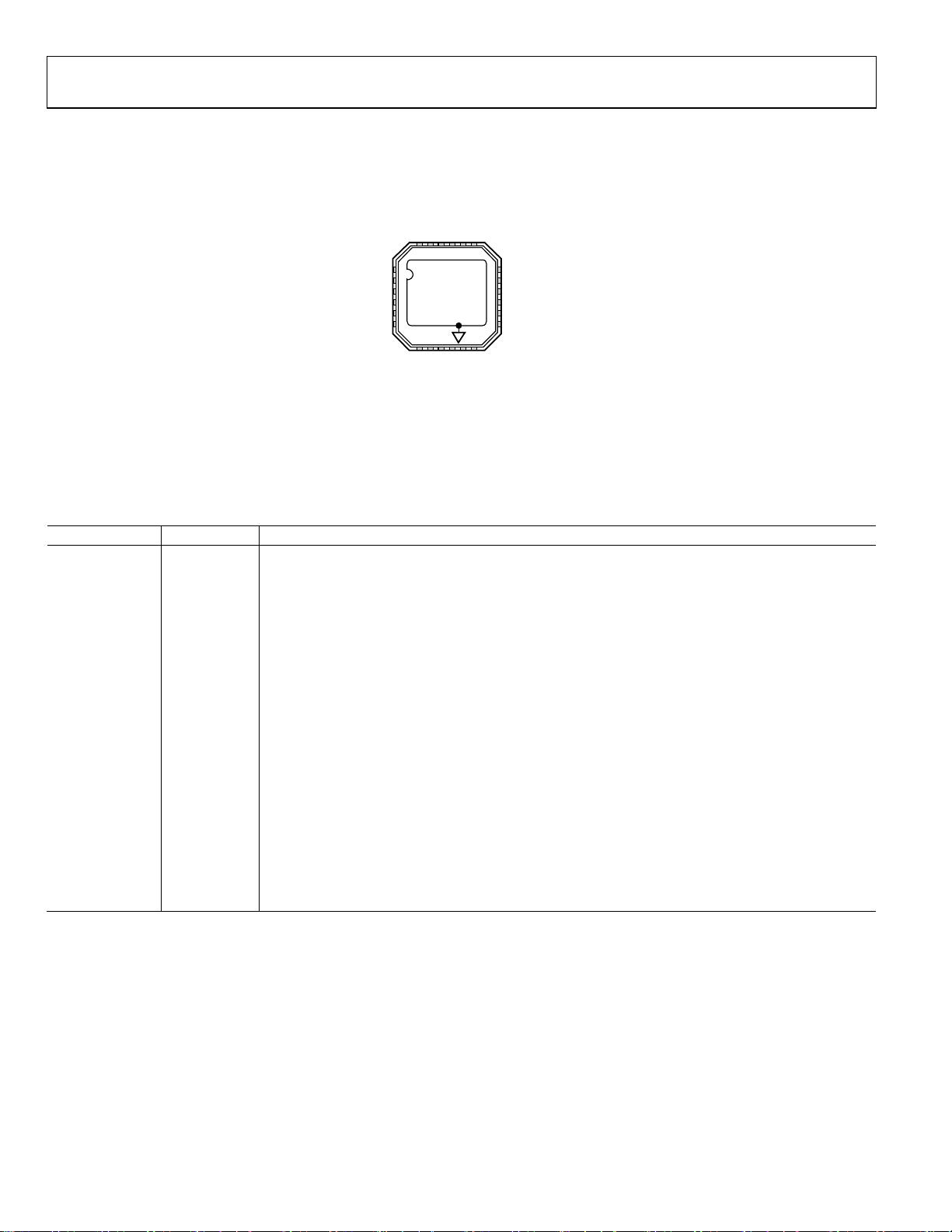
PIN CONFIGURATION AND FUNCTION DESCRIPTIONS
VPS2
IBBN
COMM
IBBP
COMM
COMM
2422232120
19
DSOP
1
COMM
LOIP
LOIN
COMM
NC
NOTES
1. NC = NO CONNECT . DO NOT CONNECT TO THIS PIN.
2. CONNECT TO THE GROUND LANE VIA A LOW
IMPEDANCE PATH.
ADL5375
2
3
TOP VIEW
4
(Not to Scale)
5
6
798
101112
NC
QBBP
QBBN
COMM
COMM
Figure 2. Pin Configuration
VPS1
18
COMM
17
RFOUT
16
NC
15
COMM
14
NC
13
COMM
07052-003
Table 3. Pin Function Descriptions
Pin No. Mnemonic Description
1 DSOP
Output Disable. A logic high on this pin disables the RF output. Connect this pin to ground or leave it
floating to enable the output.
2, 5, 8, 11, 12,
COMM Input Common Pins. Connect to the ground plane via a low impedance path.
14, 17, 19, 20, 23
3, 4 LOIP, LOIN Local Oscillator Inputs.
Single-ended operation: The LOIP pin is driven from the LO source through an ac-coupling capacitor
while the LOIN pin is ac-coupled to ground through a capacitor.
Differential operation: The LOIP and LOIN pins must be driven differentially through ac-coupling
capacitors in this mode of operation.
6, 7, 13, 15, NC No Connect. These pins can be left open or tied to ground.
9, 10, 21, 22
QBBN, QBBP,
IBBP, IBBN
Differential In-Phase and Quadrature Baseband Inputs. These high impedance inputs should be dc-
biased to the recommended level depending on the version.
ADL5375-05: 500 mV
ADL5375-15: 1500 mV
These inputs should be driven from a low impedance source. Nominal characterized ac signal swing is
500 mV p-p on each pin. This results in a differential drive of 1 V p-p. These inputs are not self-biased
and have to be externally biased.
16 RFOUT RF Output. Single-ended, 50 Ω internally biased RF output. RFOUT must be ac-coupled to the load.
18, 24 VPS1, VPS2
Positive Supply Voltage Pins. All pins should be connected to the same supply (V
). To ensure adequate
S
external bypassing, connect 0.1 μF and 100 pF capacitors between each pin and ground.
EP Exposed Paddle. Connect to the ground plane via a low impedance path.
Rev. B | Page 8 of 36
Data Sheet ADL5375
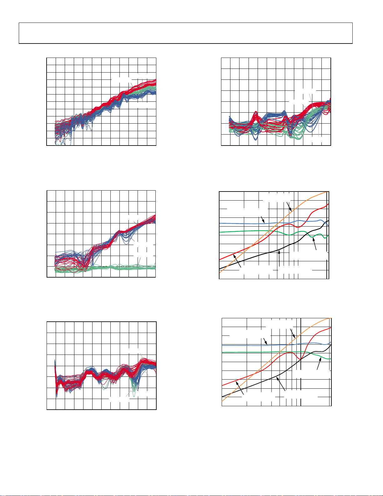
TYPICAL PERFORMANCE CHARACTERISTICS
ADL5375-05
VS = 5 V; TA = 25°C; LO = 0 dBm single-ended drive; baseband I/Q amplitude = 1 V p-p differential sine waves in quadrature with a
500 mV dc bias; baseband I/Q frequency (f
) = 1 MHz, unless otherwise noted.
BB
5
4
3
TA = –40°C
2
1
0
–1
–2
SSB OUTPUT POWER (dBm)
–3
–4
–5
0 0.5 1.0 1.5 2.0 2.5 3.0 3.5 4.0 4.5 5.0 5.5 6.0
TA = +25°C
TA = +85°C
LO FREQUENCY (GHz)
Figure 3. Single-Sideband (SSB) Output Power (P
LO Frequency (f
5
4
3
2
1
0
–1
–2
SSB OUTPUT POWER (dBm)
–3
–4
–5
0 0.51.01.52.02.53.03.54.04.55.05.56.0
) and Temperature
LO
VS = 5.25V
LO FREQ UENCY (GHz)
VS = 5.0V
VS = 4.75V
Figure 4. Single-Sideband (SSB) Output Power (P
LO Frequency (f
14
12
10
8
6
4
TA = +85°C
) and Supply
LO
TA = +25°C
TA = –40°C
OUT
OUT
) vs.
) vs.
12
VS = 5.25V
10
8
6
4
2
1dB OUTPUT COMPRESSION (dBm)
0
0 0.5 1.0 1.5 2.0 2.5 3.0 3.5 4.0 4.5 5.0 5.5 6.0
07052-052
LO FREQUE NCY (GHz)
VS = 4.75V
VS = 5.0V
07052-055
Figure 6. SSB Output 1dB Compression Point (OP1dB) vs. LO Frequency (fLO)
and Supply
90
120
150
3
400MHz
180
210
240
07052-053
Figure 7. Smith Chart of LOIP (LOIN AC-Coupled to Ground) S11 and RFOUT
400MHz
1
6GHz
4
S11
S22
270
60
1
400MHz
30
25.73 – j8.14
2
S11
6GHz
75.88 – j76.94
0
3
S22
400MHz
330
40.01 + j9.20
4
S22
6GHz
30.52 – j30.09
07052-097
2
6GHz
300
S22 from 450 MHz to 6000 MHz
0
LOIP
–5
–10
–15
–20
RETURN LOSS (dB)
RFOUT
1dB OUTPUT COMPRESSION (dBm)
2
0
0 0.51.01.52.02.53.03.54.04.55.05.56.0
LO FREQ UENCY (GHz)
07052-054
Figure 5. SSB Output 1dB Compression Point (OP1dB) vs. LO Frequency (fLO)
and Temperature
Rev. B | Page 9 of 36
–25
–30
0 0.5 1.0 1.5 2.0 2.5 3.0 3.5 4.0 4.5 5.0 5.5 6.0
FREQUE NCY (GHz )
07052-056
Figure 8. Return Loss of LOIP (LOIN AC-Coupled to Ground) S11 and RFOUT
S22 from 450 MHz to 6000 MHz
ADL5375 Data Sheet
–
–
0
–5
–10
–15
–20
–25
–30
–35
–40
–45
CARRIER FEEDTHRO UGH (dBm)
–50
–55
–60
0 0.5 1.0 1.5 2.0 2.5 3.0 3.5 4.0 4.5 5.0 5.5 6.0
LO FREQ UENCY (GHz)
TA = +85°C
= +25°C
T
A
T
= –40°C
A
07052-057
Figure 9. Carrier Feedthrough vs. LO Frequency (fLO) and Temperature;
Multiple Devices Shown
0
–10
–20
–30
–40
–50
–60
CARRIER FEE DTHROUGH (dBm)
–70
–80
0 0.5 1.0 1.5 2.0 2.5 3.0 3.5 4.0 4.5 5.0 5.5 6.0
LO FRE QUENCY (G Hz)
TA = +85°C
T
T
= –40°C
A
= +25°C
A
07052-058
Figure 10. Carrier Feedthrough vs. LO Frequency (fLO) and Temperature After
Nulling at 25°C; Multiple Devices Shown
0
–10
–20
T
= +25°C
A
TA = +85°C
T
A
= –40°C
07052-059
–30
–40
–50
–60
SIDEBAND SUPPRESSIO N (dBc)
–70
–80
0 0.5 1.0 1.5 2.0 2.5 3.0 3.5 4.0 4.5 5.0 5.5 6.0
LO FREQ UENCY (GHz)
Figure 11. Sideband Suppression vs. LO Frequency (fLO) and Temperature;
Multiple Devices Shown
0
–10
–20
–30
–40
–50
–60
SIDEBAND SUPPRESSIO N (dBc)
–70
–80
0 0.5 1.0 1.5 2.0 2.5 3.0 3.5 4.0 4.5 5.0 5.5 6.0
LO FREQ UENCY (GHz)
T
= +25°C
A
TA = +85°C
= –40°C
T
A
07052-060
Figure 12. Sideband Suppression vs. LO F requen cy (fLO) and Temperature After
Nulling at 25°C; Mul tiple Devices Shown
10
–20
–30
–40
–50
–60
–70
–80
–90
AND SIDEBAND SUPPRESSION (dBc)
DISTORTI ON, CARRIER F EEDTHROUGH,
–100
SECOND-ORDER DISTORTIO N, THIRD-ORDER
–110
0.1 2
CARRIER
FEEDTHROUG H (dBm)
THIRD-ORDER
DISTORTION (dBc)
BASEBAND INPUT VO LTAGE (V p-p)
SSB OUTPUT
POWER (d Bm)
SECOND-ORDER
DISTORTION (dBc)
SUPPRESSION (dBc)
SIDEBAND
1
10
5
0
–5
–10
–15
Figure 13. Second- and Third-Order Distortion, Carrier Feedthrough,
Sideband Suppression, and SSB P
10
–20
–30
–40
–50
–60
–70
–80
–90
AND SIDEBAND SUPPRE SSION (d Bc)
DISTORT ION, CA RRIER FEED THROUGH,
–100
SECOND-ORDE R DISTORT ION, T HIRD-ORDER
–110
0.1 2
CARRIER
FEEDTHROUG H (dBm)
THIRD-ORDER
DISTORTION (dBc)
BASEBAND INPUT V OLTAGE (V p-p )
vs. Baseband Differential Input Level
OUT
= 900 MHz)
(f
LO
SSB OUTPUT
POWER (d Bm)
SIDEBAND
SUPPRESSION (dBc)
SECOND-ORDER
DISTORTION (dBc)
1
10
5
0
–5
–10
–15
Figure 14. Second- and Third-Order Distortion, Carrier Feedthrough,
Sideband Suppression, and SSB P
vs. Baseband Differential Input Level
OUT
= 2150 MHz)
(f
LO
SSB OUTPUT POWER (dBm)
07052-061
SSB OUTPUT POWER (dBm)
07052-062
Rev. B | Page 10 of 36
Data Sheet ADL5375
–
–
–
0
–10
–20
–30
–40
–50
–60
–70
–80
AND SIDEBAND SUPPRESSION (dBc)
DISTORTI ON, CARRIER FEE DTHROUGH,
–90
SECOND-ORDER DISTO RTION, THI RD-ORDER
–100
0.1 2
CARRIER
FEEDTHROUGH (dBm)
THIRD-O RDER
DISTORTION (dBc)
BASEBAND INPUT VOLTAGE (V p- p)
SSB OUTPUT
POWER (dBm)
SECOND-ORDER
DISTORTI ON (dBc)
SIDEBAND
SUPPRESSION (dBc)
1
Figure 15. Second- and Third-Order Distortion, Carrier Feedthrough,
Sideband Suppression, and SSB P
10
–20
–30
–40
THIRD-ORDER
–50
–60
SECOND-ORDER
THIRD-ORDER DISTORTI ON (dBc)
SECOND-ORDER DISTORTI ON AND
–70
–80
0 0.5 1.0 1.5 2.0 2.5 3.0 3.5 4.0 4.5 5.0 5.5 6.0
vs. Baseband Differential Input Level
OUT
= 3500 MHz)
(f
LO
= –40°C
TA = +85°C
T
= +25°C
A
T
A
LO FREQ UENCY (GHz )
Figure 16. Second- and Third-Order Distortion vs. LO Frequency (fLO) and
Temperature (Baseband I/Q Amplitude = 1 V p-p Differential)
20
–30
–40
–50
SUPPRESSION (dBc)
CARRIER FE EDTHROUG H,
SECOND-O RDER DIST ORTI ON,
SIDEBAND SUP PRESSI ON (dB)
–60
–70
110100
SSB OUT PUT POW ER (dBm )
SIDEBAND
BASEBAND FREQUENCY (MHz)
CARRIER
FEEDTHROUGH (d Bm)
SECOND-ORDER
DISTORTI ON (dBc)
1.5
0.5
–0.5
–1.5
–2.5
–3.5
Figure 17. Second-Order Distortion, Carrier Feedthrough, Sideband
Suppression, and SSB P
vs. Baseband Frequency (fBB); fLO = 2140 MHz
OUT
10
5
0
–5
–10
–15
30
25
20
15
10
SSB OUTPUT POWE R (dBm)
07052-063
5
OUTPUT THI RD-ORDER INTERCEPT (dBm)
0
0 0.5 1.0 1.5 2.0 2.5 3.0 3.5 4.0 4.5 5.0 5.5 6.0
LO FRE QUENCY (G Hz)
Figure 18. OIP3 vs. LO Frequency (fLO) and Temperature (P
80
70
60
50
40
30
20
10
OUTPUT SECOND-O RDER INT ERCEPT (dBm)
0
0 0.5 1.0 1.5 2.0 2.5 3.0 3.5 4.0 4.5 5.0 5.5 6.0
07052-064
LO FREQ UENCY (GHz)
TA = +25°C
Figure 19. OIP2 vs. LO Frequency (fLO) and Temperature (P
20
SSB OUTPUT
POWER (dBm)
–30
CARRIER
FEEDTHROUG H (dBm)
–40
–50
–60
SSB OUTPUT POWER (dBm)
07052-098
–70
AND CARRIER FEEDT HROUGH (dBm)
SECOND-ORDER DIS TORTIO N, THIRD-O RDER
DISTORTION,SIDEBAND S UPPRESSION ( dBc),
–80
–6 –4 –2 0 2 4 6
SIDEBAND
SUPPRESSION (dBc)
LO AMPLITUDE (dBm)
DISTORTION (dBc)
SECOND-ORDER
DISTORTION (dBc)
TA = –40°C
TA = +25°C
TA = +85°C
TA = +85°C
THIRD-ORDER
≈ −5 dBm)
OUT
TA = –40°C
≈ −5 dBm)
OUT
07052-087
07052-088
2
1
0
–1
–2
SSB OUTPUT POWER (d Bm)
–3
–4
07052-065
Figure 20. Second- and Third-Order Distortion, Carrier Feedthrough,
Sideband Suppression, and SSB P
vs. LO Amplitude (fLO = 900 MHz)
OUT
Rev. B | Page 11 of 36

ADL5375 Data Sheet
–
–
20
SSB OUTPUT
–30
SECOND-ORDER DIST ORTIO N, THIRD-ORDER
DISTORTI ON,SIDEBAND SUPPRES SION (dBc),
AND CARRIER FEEDTHROUGH (d Bm)
–40
–50
–60
–70
–80
CARRIER
FEEDTHROUGH (dBm)
SIDEBAND
SUPPRESSION (dBc)
SECOND-ORDER
DISTORTION (dBc)
–6 –4 –2 0 2 4 6
LO AMPLI TUDE (dBm)
POWER (dBm)
THIRD-O RDER
DISTORTION (dBc)
Figure 21. Second- and Third-Order Distortion, Carrier Feedthrough,
Sideband Suppression, and SSB P
10
–20
–30
–40
–50
–60
AND CARRIER FEEDTHROUGH (dBm)
SECOND-ORDER DIST ORTION, THIRD-ORDER
DISTORTI ON,SIDEBAND SUPPRESSI ON (dBc),
–70
–6 –4 –2 0 2 4 6
CARRIER
FEEDTHROUGH ( dBm)
THIRD-ORDER
DISTORTION (dBc)
LO AMPLI TUDE (dBm)
vs. LO Amplitude (fLO = 2150 MHz)
OUT
SSB OUTPUT
POWER (dBm)
SIDEBAND
SUPPRESSION (dBc)
SECOND-ORDER
DISTORTIO N (dBc)
Figure 22. Second- and Third-Order Distortion, Carrier Feedthrough,
Sideband Suppression, and SSB P
vs. LO Amplitude (fLO = 3500 MHz)
OUT
2
1
0
–1
–2
SSB OUTPUT PO WER (dBm)
–3
–4
07052-066
18
16
14
12
10
8
QUANTITY
6
4
2
0
–160.5 –160.3 –160.1 –159.9 –159.7 –159.5 –159.3 –159.1
NOISE (dBm/Hz)
07052-089
Figure 24. 20 MHz Offset Noise Floor Distribution at fLO = 900 MHz
(I/Q Amplitude = 0 mV p-p with 500 mV DC Bias)
1
0
–1
–2
–3
SSB OUTPUT POWER (dBm)
–4
–5
07052-067
8
7
6
5
4
QUANTITY
3
2
1
0
–160.5 –1 60.1 –159. 7 –159.3 –158.9 –158.5
NOISE (d Bm/Hz)
07052-090
Figure 25. 20 MHz Offset Noise Floor Distribution at fLO = 2140 MHz
(I/Q Amplitude = 0 mV p-p with 500 mV DC Bias)
210
205
200
195
190
185
180
SUPPLY CURRENT (mA)
175
170
165
–40 25 85
VS = 5.25V
= 5.0V
V
S
= 4.75V
V
S
TEMPERATURE (°C)
Figure 23. Power Supply Current vs. Temperature
07052-068
10
9
8
7
6
5
QUANTIT Y
4
3
2
1
0
–158.9 –158.5 –158.1 –157.7 –157.3 –156.9 –156.5
NOISE (dBm/Hz)
Figure 26. 20 MHz Offset Noise Floor Distribution at fLO = 3500 MHz
07052-099
(I/Q Amplitude = 0 mV p-p with 500 mV DC Bias)
Rev. B | Page 12 of 36

Data Sheet ADL5375
86
88
85
83
82
81
80
79
SSB OUTP UT POW ER ISOLATIO N (dB)
78
0 0.5 1.0 1. 5 2.0 2.5 3.0 3.5 4.0 4.5 5. 0 5.5 6.0
Figure 27. SSB P
SSB OUT PUT PO WER IS OLAT ION (d B)
CARRIER FEEDTHROUG H (dBm)
LO FREQUENCY ( GHz)
Isolation and Carrier Feedthrough with DSOP High
OUT
0
–10
–20
–30
–40
–50
–60
CARRIER FE EDTHROUG H (dBm)
–70
–80
07052-091
Rev. B | Page 13 of 36

ADL5375 Data Sheet
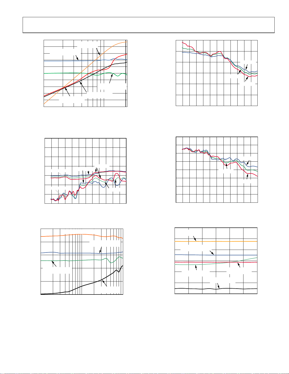
ADL5375-15
VS = 5 V; TA = 25°C; LO = 0 dBm single-ended drive; baseband I/Q amplitude = 1 V p-p differential sine waves in quadrature with a
1500 mV dc bias; baseband I/Q frequency (f
5
4
3
2
TA = –40°C
1
0
–1
–2
SSB OUTP UT POWER (dBm)
–3
–4
–5
0 0.5 1.0 1.5 2. 0 2.5 3.0 3.5 4.0 4. 5 5.0 5.5 6.0
Figure 28. Single-Sideband (SSB) Output Power (P
5
4
3
2
1
0
–1
–2
SSB OUTP UT POWER (dBm)
–3
–4
–5
0 0.5 1.0 1.5 2. 0 2.5 3.0 3.5 4.0 4. 5 5.0 5.5 6.0
Figure 29. Single-Sideband (SSB) Output Power (P
TA = +25°C
TA = +85°C
LO FREQUENCY (GHz)
and Temperature
LO FREQUENCY (GHz)
) and Supply
(f
LO
) = 1 MHz, unless otherwise noted.
BB
07052-069
) vs. LO Frequency (fLO)
OUT
VS = 4.75V
VS = 5.0V
VS = 5.25V
) vs. LO Frequency
OUT
07052-070
12
10
8
6
4
2
1dB OUTPUT COMPRE SSION (dBm)
0
VS = 5.25V
VS = 4.75V
0 0.5 1.0 1.5 2. 0 2.5 3.0 3.5 4.0 4. 5 5.0 5.5 6.0
LO FREQUENCY (GHz)
VS = 5.0V
07052-072
Figure 31. SSB Output 1dB Compression Point (OP1dB) vs. LO Frequency (fLO)
and Supply
90
2
6GHz
60
300
30
330
0
S11
1
400MHz
25.07 – j7.11
2
S11
6GHz
96.98 – j74.75
3
S22
400MHz
38.63 + j10. 34
4
S22
6GHz
34.35 – j30.63
180
150
210
120
240
400MHz
1
6GHz
400MHz
3
4
S11
S22
270
Figure 32. Smith Chart of LOIP (LOIN AC-Coupled to Ground) S11 and RFOUT
S22 from 450 MHz to 6000 MHz
07052-102
12
10
TA = +25°C
8
6
4
2
1dB OUTPUT COMPRE SSION ( dBm)
0
0 0.5 1.0 1.5 2.0 2. 5 3.0 3.5 4.0 4. 5 5.0 5.5 6.0
LO FREQUENCY (GHz)
TA = –40°C
TA = +85°C
07052-071
Figure 30. SSB Output 1dB Compression Point (OP1dB) vs. LO Frequency (fLO)
and Temperature
Rev. B | Page 14 of 36
0
–5
LOIP
–10
–15
–20
RETURN LO SS (dB)
–25
–30
0 0.5 1.0 1.5 2. 0 2.5 3.0 3.5 4.0 4. 5 5.0 5.5 6.0
FREQUENCY (GHz)
RFOUT
07052-073
Figure 33. Return Loss of LOIP (LOIN AC-Coupled to Ground) S11 and RFOUT
S22 from 450 MHz to 6000 MHz

Data Sheet ADL5375
0
–5
–10
–15
–20
–25
–30
–35
–40
–45
CARRIER FEEDTHRO UGH (dBm)
–50
–55
–60
0 0.5 1.0 1.5 2.0 2.5 3.0 3.5 4.0 4.5 5.0 5.5 6.0
LO FREQUENCY (GHz)
TA = +85°C
T
= +25°C
A
= –40°C
T
A
Figure 34. Carrier Feedthrough vs. LO Frequency (fLO) and Temperature;
Multiple Devices Shown
07052-074
0
–10
–20
–30
–40
–50
–60
SIDEBAND SUPPRESSI ON (dBc)
–70
–80
0 0.5 1. 0 1.5 2.0 2. 5 3.0 3.5 4.0 4.5 5. 0 5.5 6.0
T
A
LO FREQUENCY (GHz)
= –40°C
= +25°C
T
A
TA = +85°C
07052-077
Figu re 37. Sideband Suppression vs. LO Freque ncy (fLO) and Temperature After
Nulling at 25°C; Mul tiple Devices Shown
0
–10
–20
–30
–40
–50
–60
CARRIER FEEDTHRO UGH (dBm)
–70
–80
0 0.5 1.0 1.5 2.0 2.5 3.0 3.5 4.0 4.5 5.0 5.5 6.0
T
= –40°C
A
TA = +85°C
LO FREQUENCY (GHz)
TA = +25°C
07052-075
Figure 35. Carrier Feedthrough vs. LO Frequency (fLO) and Temperature After
Nulling at 25°C; Multiple Devices Shown
0
–10
–20
–30
= +25°C
T
–40
–50
–60
SIDEBAND SUPPRESSION (dBc)
–70
–80
0 0.5 1.0 1.5 2.0 2.5 3.0 3.5 4.0 4.5 5.0 5.5 6.0
A
LO FREQUENCY (GHz)
T
= –40°C
A
TA = +85°C
07052-076
Figure 36. Sideband Suppression vs. LO Frequency (fLO) and Temperature;
Multiple Devices Shown
0
–10
–20
–30
SUPPRESSION (dBc)
–40
–50
–60
–70
–80
AND SIDEBAND SUPP RESSION (dBc)
DISTORT ION, CA RRIER FEE DTHROUGH,
–90
SECOND-ORDER DISTO RTION, THIRD-O RDER
–100
0.1
CARRIER
FEEDTHRO UGH (dBm)
SIDEBAND
BASEBAND INPUT VOLTAGE (V p-p)
SSB OUTPUT
POWER (dBm)
DISTORTION (dBc)
SECOND-ORDER
DISTORT ION (d Bc)
THIRD-ORDER
1
Figure 38. Second- and Third-Order Distortion, Carrier Feedthrough,
Sideband Suppression, and SSB P
0
–10
–20
–30
–40
SUPPRESSION (dBc)
–50
–60
–70
–80
AND SIDEBAND SUPPRESSION ( dBc)
DISTORTI ON, CARRIER FEEDT HROUGH,
–90
SECOND-ORDER DISTORTION, THIRD-ORDER
–100
0.1
CARRIER
FEEDTHROUGH (dBm)
SIDEBAND
BASEBAND INPUT VOLTAGE (V p-p)
vs. Baseband Differential Input Level
OUT
= 900 MHz)
(f
LO
SSB OUTPUT
POWER (dBm)
SECOND-ORDER
THIRD-ORDER
DISTORTION (dBc)
DISTORTION (dBc)
1
Figure 39. Second- and Third-Order Distortion, Carrier Feedthrough,
Sideband Suppression, and SSB P
vs. Baseband Differential Input Level
OUT
= 2150 MHz)
(f
LO
10
5
0
–5
–10
–15
10
5
0
–5
–10
–15
SSB OUTPUT POWER (dBm)
07052-078
SSB OUTPUT PO WER (dBm)
07052-079
Rev. B | Page 15 of 36

ADL5375 Data Sheet
–
–
0
–10
–20
–30
–40
–50
–60
–70
–80
AND SIDEBAND SUPPRESSI ON (dBc)
DISTORTI ON, CARRIER FEEDTHROUGH,
–90
SECOND-ORDER DIS TORTIO N, THIRD-O RDER
–100
CARRIER
FEEDTHROUG H (dBm)
SIDEBAND
SUPPRESSION (dBc)
0.1
BASEBAND INPUT VOL TAGE (V p -p)
SSB OUTPUT
POWER (dBm)
THIRD-ORDER
DISTORTI ON (dBc)
SECOND-ORDER
DISTORTION (dBc)
1
Figure 40. Second- and Third-Order Distortion, Carrier Feedthrough,
Sideband Suppression, and SSB P
0
vs. Baseband Differential Input Level
OUT
(f
= 3500 MHz)
LO
10
5
0
–5
–10
–15
30
28
26
24
22
20
18
16
14
12
10
SSB OUTPUT POWER (dBm)
07052-080
8
6
4
OUTPUT THIRD-ORDER INTERCEPT (dBm)
2
0
0 0.5 1.0 1.5 2.0 2. 5 3.0 3.5 4.0 4.5 5. 0 5. 5 6.0
LO FREQUENCY (GHz)
TA = +25°C
Figure 43. OIP3 vs. LO Frequency (fLO) and Temperature (P
= 900 MHz)
f
LO
70
TA = –40°C
TA = +85°C
≈ −5 dBm @
OUT
07052-092
–10
–20
–30
–40
–50
–60
THIRD-ORD ER DISTO RTION ( dBc)
SECOND-ORDE R DISTORT ION AND
–70
–80
TA = +25°C
0 0.5 1.0 1.5 2.0 2.5 3.0 3. 5 4.0 4.5 5.0 5.5 6.0
LO FREQUENCY (GHz)
= –40°C
T
A
THIRD-ORDER
TA = +85°C
SECOND-ORDE R
07052-081
Figure 41. Second- and Third-Order Distortion vs. LO Frequency (fLO) and
Temperature (Baseband I/Q Amplitude = 1 V p-p Differential)
20
–30
–40
–50
SIDEBAND SUPPRESSION
CARRIER FE EDTHROU GH,
SECOND-O RDER DIS TORTI ON,
–60
–70
SSB OUTPUT POWER (dBm)
SIDEBAND
SUPPRESSION (dBc)
CARRIER
FEEDTHROUGH (dBm)
SECOND-O RDER
DISTORTION (dBc)
110100
BASEBAND FREQUENCY (MHz)
1.5
0.5
–0.5
–1.5
–2.5
–3.5
SSB OUTPUT POWER (dBm)
Figure 42. Second-Order Distortion, Carrier Feedthrough, Sideband
Suppression, and SSB P
vs. Baseband Frequency (fBB); fLO = 2140 MHz
OUT
60
50
40
30
20
10
OUTPUT SECOND-ORDER INTERCEPT (dBm)
0
0 0.5 1.0 1.5 2.0 2.5 3. 0 3.5 4.0 4.5 5.0 5.5 6.0
LO FREQUENCY (GHz)
TA = +25°C
Figure 44. OIP2 vs. LO Frequency (fLO) and Temperature (P
f
= 900 MHz)
LO
20
–30
–40
–50
–60
–70
–80
AND SIDEBAND SUPPRESSION (d Bc)
DISTORTI ON, CARRIER FEEDT HROUGH,
SECOND-ORDER DISTO RTION, T HIRD-ORDER
07052-103
SECOND-ORDER
DISTORTI ON (dBc)
–90
–6 –4 –2 0 2 4 6
CARRIER
FEEDTHROUGH (dBm)
SIDEBAND
SUPPRESSION (dBc)
LO AMPL ITUDE (dBm)
SSB OUTPUT
POWER (dBm)
TA = –40°C
TA = +85°C
≈ −5 dBm @
OUT
THIRD-ORDER
DISTORTION (dBc)
07052-093
2
1
0
–1
SSB OUTPUT PO WER (dBm)
–2
07052-082
Figure 45. Second- and Third-Order Distortion, Carrier Feedthrough,
Sideband Suppression, and SSB P
vs. LO Amplitude (fLO = 900 MHz)
OUT
Rev. B | Page 16 of 36

Data Sheet ADL5375
–
–
20
–30
–40
–50
–60
–70
AND SIDEBAND SUPPRESSION (dBc)
DISTORTI ON, CARRIER FEEDT HROUGH,
SECOND-ORDER DISTO RTION, T HIRD-ORDER
–80
–6 –4 –2 0 2 4 6
CARRIER
FEEDTHROUGH (d Bm)
SIDEBAND
SUPPRESSION (dBc)
DISTORTI ON (dBc)
LO AMPLI TUDE (dBm)
SSB OUTPUT
POWER (dBm)
THIRD-O RDER
SECOND-ORDER
DISTORTION (dBc)
Figure 46. Second- and Third-Order Distortion, Carrier Feedthrough,
Sideband Suppression, and SSB P
vs. LO Amplitude (fLO = 2150 MHz)
OUT
2
1
0
–1
SSB OUTPUT POWER (dB m)
–2
07052-083
18
16
14
12
10
8
QUANTITY
6
4
2
0
–158.0 –157.8 –157.6 –157.4 –157.2 –157.0 –156.8 –156.6
NOISE ( dBm/Hz)
Figure 49. 20 MHz Offset Noise Floor Distribution at fLO = 900 MHz
(I/Q Amplitude = 0 mV p-p with 1500 mV DC Bias)
07052-094
20
–30
SSB OUTPUT
POWER (dBm)
–40
–50
–60
THIRD-O RDER
DISTORTION (dBc)
–70
AND SIDEBAND SUPPRESSION (d Bc)
DISTORTI ON, CARRIER FEEDT HROUGH,
SECOND-ORDER DIST ORTION, THIRD-ORDER
–80
–6 –4 –2 0 2 4 6
LO AMPLI TUDE (dBm)
CARRIER
FEEDTHROUGH (d Bm)
SIDEBAND
SUPPRESSION (dBc)
SECOND-ORDER
DISTORTION (dBc)
Figure 47. Second- and Third-Order Distortion, Carrier Feedthrough,
Sideband Suppression, and SSB P
0.230
0.220
0.210
0.200
0.190
0.180
SUPPLY CURRENT (A)
0.170
0.160
–40 25 85
vs. LO Amplitude (fLO = 3500 MHz)
OUT
= 5.25V
V
S
V
= 5.0V
S
V
= 4.75V
S
TEMPERATURE (°C)
Figure 48. Power Supply Current vs. Temperature
2.0
1.5
1.0
0.5
0
–0.5
–1.0
–1.5
–2.0
12
10
8
6
QUANTIT Y
4
SSB OUTPUT POW ER (dBm)
07052-084
2
0
–158.5 –158.3 –158.1 –157.9 –157.7 –157.5 –157.3 –157.1
NOISE (dBm/Hz)
07052-095
Figure 50. 20 MHz Offset Noise Floor Distribution at fLO = 2140 MHz
(I/Q Amplitude = 0 mV p-p with 1500 mV DC Bias)
9
8
7
6
5
4
QUANTIT Y
3
2
1
0
–157.5 –157.1 –156.7 –156. 3 –155.9 –155.5
07052-085
NOISE ( dBm/Hz)
07052-104
Figure 51. 20 MHz Offset Noise Floor Distribution at fLO = 3500 MHz
(I/Q Amplitude = 0 mV p-p with 500 mV DC Bias)
Rev. B | Page 17 of 36

ADL5375 Data Sheet
88
86
84
82
80
78
76
SSB OUTPUT P OWER IS OLATIO N (dB)
74
Figure 52. SSB P
SSB OUTPUT POW ER ISOLATION (dB)
CARRIER FE EDTHRO UGH (dBm)
0 0.5 1.0 1.5 2.0 2.5 3.0 3.5 4.0 4.5 5.0 5.5 6.0
LO FRE QUENCY (GHz)
Isolation and Carrier Feedthrough with DSOP High
OUT
0
–10
–20
–30
–40
–50
–60
–70
–80
–90
CARRIER FEEDTHRO UGH (dBm)
07052-096
Rev. B | Page 18 of 36
Data Sheet ADL5375
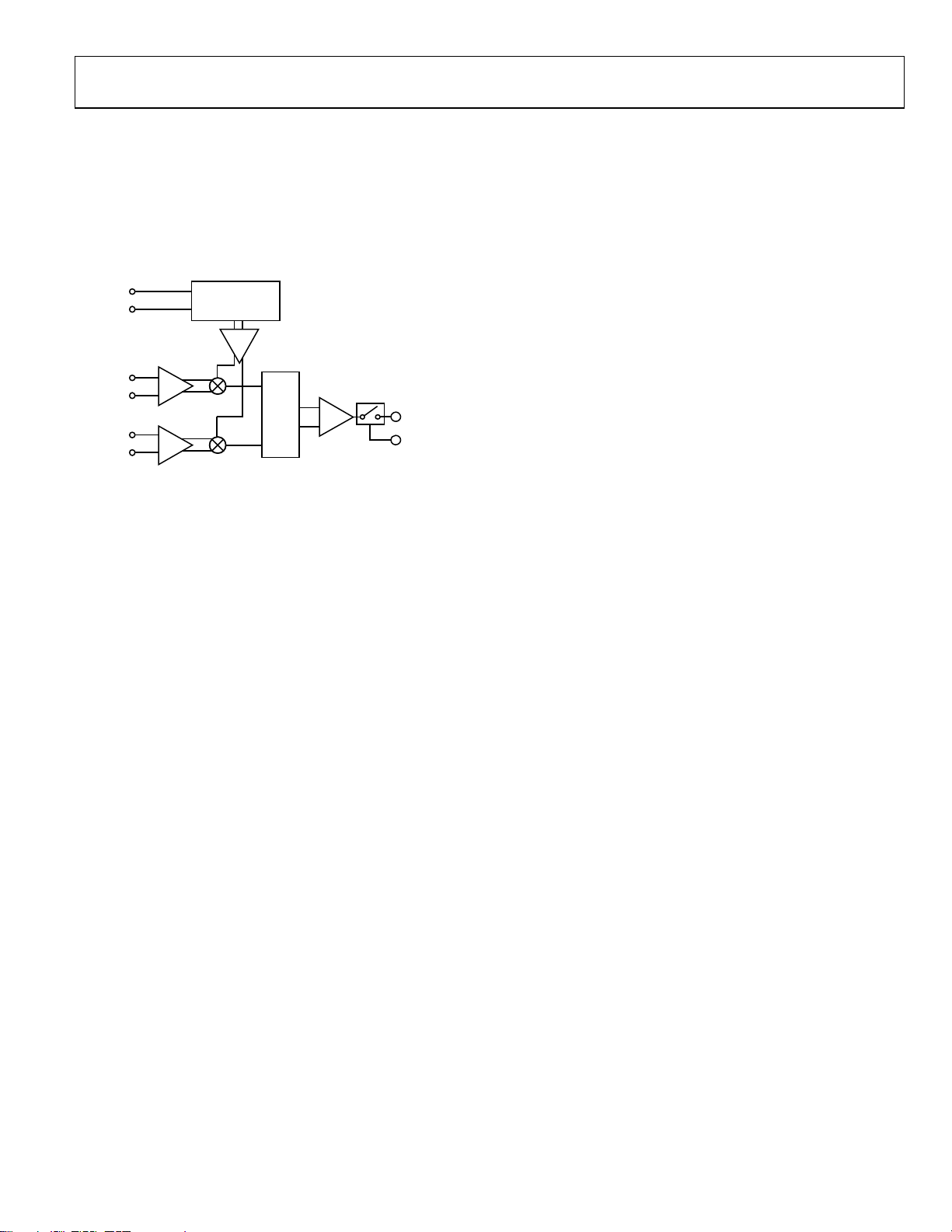
THEORY OF OPERATION
CIRCUIT DESCRIPTION
The ADL5375 can be divided into five circuit blocks: the LO
interface, the baseband voltage-to-current (V-to-I) converter,
the mixers, the differential-to-single-ended (D-to-S) stage,
and the bias circuit. A block diagram of the device is shown in
Figure 53.
LOIP
LOIN
IBBP
IBBN
QBBP
QBBN
The LO interface generates two LO signals in quadrature.
These signals are used to drive the mixers. The I/Q baseband
input signals are converted to currents by the V-to-I stages,
which then drive the two mixers. The outputs of these mixers
combine to feed the output balun, which provides a singleended output. The bias cell generates reference currents for
the V-to-I stage.
LO Interface
The LO interface consists of a polyphase quadrature splitter
and a limiting amplifier. The LO input impedance is set by
the polyphase splitter. Each quadrature LO signal then passes
through a limiting amplifier that provides the mixer with a
limited drive signal.
The LO input can be driven single-ended or differentially.
For applications above 3 GHz, improved OIP2 and LO leakage
may result from driving the LO input differentially.
PHASE
SPLITTER
Figure 53. Block Diagram
RFOUT
DSOP
07052-028
V-to-I Converter
The differential baseband inputs (QBBP, QBBN, IBBN, and
IBBP) present a high impedance. The voltages applied to these
pins drive the V-to-I stage that converts baseband voltages into
currents. The differential output currents of the V-to-I stages
feed each of their respective mixers. The dc common-mode
voltage at the baseband inputs sets the currents in the two
mixer cores. Varying the baseband common-mode voltage
influences the current in the mixer and affects overall modulator performance. The recommended dc voltage for the baseband
common-mode voltage is 500 mV dc for the ADL5375-05 and
1500 mV for the ADL5375-15.
Mixers
The ADL5375 has two double-balanced mixers: one for the
in-phase channel (I channel) and one for the quadrature channel (Q-channel). The output currents from the two mixers sum
together into an internal load. The signal developed across this
load is used to drive the D-to-S stage.
D-to-S Stage
The output D-to-S stage consists of an on-chip active balun
that converts the differential signal to a single-ended signal.
The balun presents 50 impedance to the output (VOUT).
Therefore, no matching network is needed at the RF output
for optimal power transfer in a 50 environment.
Bias Circuit
An on-chip band gap reference circuit is used to generate a
proportional-to-absolute temperature (PTAT) reference current
for the V-to-I stage.
DSOP
The DSOP pin can be used to disable the output stage of the
modulator. If the DSOP pin is connected to ground or left
unconnected, the part operates normally. If the DSOP pin is
connected to the positive voltage supply, the output stage is
disabled and the LO leakage is also reduced.
Rev. B | Page 19 of 36

ADL5375 Data Sheet
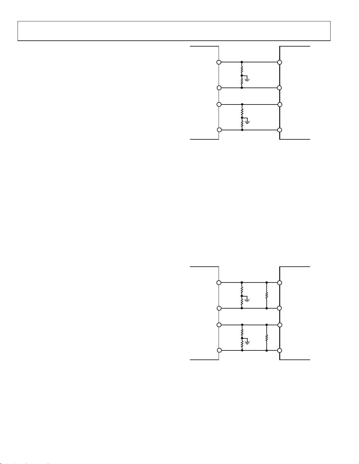
BASIC CONNECTIONS
IBBN
IBBP
LOIP
VPOS
VPOS
S1
C6
100pF
100pF
C5
0.1µF
BA
C7
DSOP
COMM
LOIP
LOIN
COMM
NC
C3
100pF
VPS2
COMM
2423222120
1
2
3
4
5
6
QBBN QBBP
Figure 54. Basic Connections for the ADL5375
ADL5375
EXPOSED PADDLE
7
8
NC
COMM
Figure 54 shows the basic connections for the ADL5375.
POWER SUPPLY AND GROUNDING
Pin VPS1 and Pin VPS2 should be connected to the same 5 V
source. Each pin should be decoupled with a 100 pF and
0.1 F capacitor. These capacitors should be located as close
as possible to the device. The power supply can range between
4.75 V and 5.25 V.
The ten COMM pins should be tied to the same ground plane
through low impedance paths.
The exposed paddle on the underside of the package should
also be soldered to a ground plane with low thermal and
electrical impedance. If the ground plane spans multiple layers
on the circuit board, they should be stitched together with nine
vias under the exposed paddle as illustrated in the Evaluation
Board section. The AN-772 Application Note discusses the
thermal and electrical grounding of the LFCSP (QFN) package
in detail.
BASEBAND INPUTS
The baseband inputs (IBBP, IBBN, QBBP, and QBBN) should be
driven from a differential source. The nominal drive level used
in the characterization of the ADL5375 is 1 V p-p differential
(or 500 mV p-p on each pin).
IBBN
Z1
9
QBBN
IBBP
COMM
COMM
101112
QBBP
COMM
19
C2
VPS1
18
COMM
17
RFOUT
16
NC
15
COMM
14
13
NC
COMM
100pFC40.1µF
C1
100pF
GND
VPOS
RFOUT
All the baseband inputs must be externally dc biased. The
recommended common-mode level is dependent on the
version of the ADL5375.
ADL5375-05: 500 mV
ADL5375-15: 1500 mV
LO INPUT
The LO input is designed to be driven from a single-ended
source. The LO source is ac-coupled through a series capacitor
to the LOIP pin while the LOIN pin is ac-coupled to ground
through a second capacitor.
The typical LO drive level, which was used for the characterization
of the ADL5375, is 0 dBm.
Differential operation is also possible, in which case both sides
of the differential LO source should be ac-coupled through a
pair of series capacitors to the LOIP and LOIN pins.
RF OUTPUT
The RF output is available at the RFOUT pin (Pin 16), which can
drive a 50 load. The internal balun provides a low dc path to
ground. In most situations, the RFOUT pin must be ac-coupled
to the load.
07052-029
Rev. B | Page 20 of 36

Data Sheet ADL5375
OUTPUT DISABLE
The ADL5375 incorporates an output disable pin feature that
shuts down the output amplifier stage to isolate the modulator
from the load. This output is disabled when the voltage on the
DSOP exceeds 2 V. The output is enabled when the DSOP pin is
either tied to ground or left unconnected.
Asserting DSOP further reduces LO leakage (see Figure 27 and
Figure 52) and drives the broadband noise of the device down
to just above the KT thermal noise level. Asserting DSOP also
reduces the supply current of the ADL5375 from 200 mA to
127 mA.
The time delay between when DSOP pin going low and the
output power being restored is approximately 200 ns. The time
delay when DSOP going high and output being disabled is less
than 100 ns.
Rev. B | Page 21 of 36

ADL5375 Data Sheet
–
APPLICATIONS INFORMATION
CARRIER FEEDTHROUGH NULLING
LO leakage results from minute dc offsets that occur on the
differential baseband inputs. In an IQ modulator, non-zero
differential offsets mix with the LO and result in LO leakage to
the RF output. In addition to this effect, some of the signal
power at the LO input couples directly to the RF output (this
may be a result of bond-wire to bond-wire coupling or coupling
through the silicon substrate). The net LO leakage at the RF
output is the vector combination of the signals that appear at
the output as a result of these two effects.
The device’s nominal carrier feedthrough can be nulled by
adding small external differential offset voltages on the I and Q
inputs.
Nulling the carrier feedthrough is a multistep process. Initially,
with the I-channel offset held constant (at 0 mV), the Qchannel offset is varied until a minimum LO leakage level is
obtained. This Q-channel offset voltage is then held constant,
while the offset on the I-channel is adjusted until a new
minimum is reached. Through two iterations of this process,
the LO leakage can be reduced to an arbitrarily low level. This
level is only limited by the available offset voltage steps and by
the modulator’s noise floor. Figure 55 illustrates the typical
relationship between LO leakage and dc offset at 1900 MHz. In
this case, differential offset voltages of approximately +0.5 mV
and −0.5 mV on the I and Q inputs, respectively, result in the
lowest carrier feedthrough. It is important to note that the
required offset nulling voltage changes in polarity and
magnitude from device to device and overtemperature and
frequency. To ensure that all devices in a mass production
environment can be adequately nulled, an offset adjustment
range of approximately ±10 mV should be provided.
57
Q OFFSET SWEEP I OFFSET SWEEP
–62
–67
–72
–77
–82
CARRIER FEEDTHROUGH (dBm)
–87
–92
–1.0 –0.8 –0.6 –0.4 –0.2 0 0.2 0.4 0.6 0.8 1.0
Figure 55. Example of Typical Carrier Feedthrough vs. DC Offset Voltage
It is important to note that the carrier feedthrough is not
affected by the dc bias levels (also called the common-mode
level) on the I and Q inputs. A differential offset voltage must
be applied, so after nulling, the average voltage on the IP and
I AND Q OFFSET VOLTAGE (µV)
Rev. B | Page 22 of 36
07052-031
IN inputs can be slightly different. Using Figure 55 as an
example, after LO leakage nulling, the average dc level on IP
and IN can be 500.25 mV and 499.75 mV.
The same applies to the Q-channel. For the ADL5375-15, the
same theory applies except that
V
= V
IBBP
= 1500 mV.
IBBN
It is often desirable to perform a one-time carrier null. This is
usually performed at a given frequency. After this factory
calibration, the IQ modulator operates over a frequency range
on each side of the calibration frequency. The nulled LO leakage
level degrades somewhat because the LO frequency is moved
away from the calibration frequency. Despite this degradation,
the overall LO leakage across a frequency band can be expected
to be better than when no nulling is performed. This assumes
an operating frequency band that is in the 30 MHz to 60 MHz
range.
LO leakage nulling is discussed further in AN-1039, Correcting
Imperfections in IQ Modulators to Improve RF Signal Fidelity.
SIDEBAND SUPPRESSION OPTIMIZATION
Sideband suppression results from relative gain and relative
phase offsets between the I-channel and Q-channel and can
be suppressed through adjustments to those two parameters.
Figure 56 illustrates how sideband suppression is affected by
the gain and phase imbalances.
0
–10
2.5dB
–20
1.25dB
0.5dB
–30
0.25dB
–40
0.125dB
0.05dB
–50
0.025dB
–60
0.0125dB
–70
SIDEBAND SUPPRESSI ON (dBc)
0dB
–80
–90
0.01 0.1 1 10 100
Figure 56. Sideband Suppression vs. Quadrature Phase Error for
Various Quadrature Amplitude Offsets
Figure 56 underlines the fact that adjusting only one parameter
improves the sideband suppression only to a point, unless the
other parameter is also adjusted. For example, if the amplitude
offset is 0.25 dB, improving the phase imbalance by better than
1° does not yield any improvement in the sideband suppression.
For optimum sideband suppression, an iterative adjustment
between phase and amplitude is required.
The sideband suppression nulling can be performed either
through adjusting the gain for each channel or through the
modification of the phase and gain of the digital data coming
from the baseband signal processor.
PHASE ERROR (Deg rees)
07052-032

Data Sheet ADL5375
V
Sideband suppression is discussed further in AN-1100, Wireless
Transmitter IQ Balance and Sideband Suppression, as well as in
AN-1039, Correcting Imperfections in IQ Modulators to Improve
RF Signal Fidelity.
INTERFACING THE ADF4350 PLL TO THE ADL5375
With an output frequency range of 137.5 to 4.4 GHz, a high
performance integrated VCO and an LO output power level
that can be programmed from −4 dBm to +5 dBm, the
ADF4350 wideband synthesizer is ideally suited to drive the
ADL5375 LO port.
Care must be taken to adequately suppress the harmonics of the
LO signal from the PLL. VCOs typically have a third harmonic
power of approximately −10 dBc. A large third harmonic on the
LO degrades the quality of the quadrature generation inside the
IQ Modulator. The third harmonic should be suppressed to a
level of –30 dBc or lower to prevent quadrature degradation. So
approximately 20 dB of attenuation is required to get the third
harmonic below −30 dBc. Figure 57 shows PLL modulator
interfaces schematic that for this operation at four different
frequencies, and Table 4 shows the optimized components value
of Figure 57. Because filtering of the third harmonic is most
critical, and to ensure wide frequency range coverage, the 3 dB
corner of the filters have been set to approximately 1.2~1.5
times the maximum desired LO frequency. A Chebyshev filter
topology at 100 Ω differential source impedance and 50 Ω
differential load impedance was used for optimal performance.
3.3
120pF120pF
0.1µF
C1a
C2a
C2c
C2a
C3a
C3c
C3a
1nF
1nF
3
LOIP
4
LOIN
ADL5375
RF
A+
OUT
RF
A–
OUT
ADF4350
Z
BIAS
12
R1
Z
BIAS
13
L1 L2
C1c
L1 L2
C1a
Figure 57. PLL-Modulator Interface Schematic
07052-111
Table 4. PLL Modulator Interface Components Values (DNI = Do Not Insert)
Frequency Range (MHz) Zbias (nH) R1 (Ω) L1 (nH) L2 (nH) C1a (pF) C1c (pF) C2a C2c (pF) C3a (pF) C3c (pF)
500 to 1300 27 100 3.9 3.9 DNI 4.7 DNI 5.6 DNI 3.3
850 to 2450 19 100 2.7 2.7 3.3 DNI 4.7 DNI 3.3 DNI
1250 to 2800 7.5 100 0 Ω 3.6 DNI DNI 2.2 DNI 1.5 DNI
2800 to 4400 3.9 100 0 Ω 0 Ω DNI DNI DNI DNI DNI DNI
Rev. B | Page 23 of 36
ADL5375 Data Sheet
The two pull-up inductors of the Zbias provide two 50 Ω source
impedances in combination with R1 resistor in parallel for the
filter. While the ADL5375 is specified to be driven by a singleended LO, the LOIP and LOIN input pins are naturally
differential. Therefore, the differential LO drive from the
ADF4350 is more desirable.
The output power from the ADF4350 can be set to −4 dBm,
−1 dBm,+2 dBm, and +5 dBm using Register 4 Bits[D2:D1] and
−6 dBm to +7 dBm LO drive level for ADL5375 is recommended.
If the physical distance between the PLL and the IQ modulator
is significant, the filter should be placed adjacent to the IQ
modulator, and two 50 Ω traces should be run between the
devices (since there is a 50 Ω impedance looking from each of
the filter inputs back to each of the PLL outputs).
The ADL5375 evaluation board can be reconfigured for
differential drive and also includes component pads in its LO
path to accommodate a harmonic filter. The ADF4350 evaluation
board can also be configured to provide a differential output and
can be connected directly to the ADL5375 evaluation board.
Optimizing the interface between a PLL LO and I/Q modulator
is discussed further in CN-0134 Broadband Low EVM Direct
Conversion Transmitter: How to Optimize the Interface
Between a PLL LO and I/Q Modulator.
DAC MODULATOR INTERFACING
Driving the ADL5375-05 with a TXDAC®
The ADL5375-05 is designed to interface with minimal
components to members of the Analog Devices, Inc. TxDAC
families. These dual-channel differential current output DACs
feature an output current swing from 0 mA to 20 mA. The
interface described in this section can be used with any DAC
that has a similar output.
An example of an interface using the AD9122 TxDAC is shown
in Figure 58. The baseband inputs of the ADL5375-05 require a
dc bias of 500 mV. The nominal midscale current on each of the
outputs of the AD9122 is 10 mA. Therefore, a single 50 Ω resistor to ground from each of the DAC outputs results in an average
current of 10 mA flowing through each of the resistors, thus
producing the desired 500 mV dc bias for the inputs to the
ADL5375-05.
AD9122
IOUT1P
IOUT1N
IOUT2N
IOUT2
Figure 58. Interface Between the AD9122 and ADL5375-05 with 50 Ω
Resistors to Ground to Establish the 500 mV DC Bias for the ADL5375-05
67
66
59
58
RBIP
50
RBIN
50
RBQN
50
RBQP
50
Baseband Inputs
ADL5375-05
21
IBBP
22
IBBN
9
QBBN
10
QBBP
07052-112
The AD9122 output currents have a swing that ranges from 0 mA
to 20 mA. With the 50 Ω resistors in place, the ac voltage swing
going into the ADL5375-05 baseband inputs ranges from 0 V to
1 V. A full-scale sine wave out of the AD9122 can be described
as a 1 V p-p single-ended (or 2 V p-p differential) sine wave
with a 500 mV dc bias.
Limiting the AC Swing
There are situations in which it is desirable to reduce the ac
voltage swing for a given DAC output current. This can be
achieved through the addition of another resistor to the interface.
This resistor is placed in the shunt between each side of the
differential pair, as shown in Figure 59. It has the effect of
reducing the ac swing without changing the dc bias already
established by the 50 Ω resistors.
AD9122
IOUT1P
IOUT1N
IOUT2N
IOUT2
Figure 59. AC Voltage Swing Reduction Through the Introduction
67
RBIP
50
RBIN
66
50
59
RBQN
50
RBQP
58
50
of a Shunt Resistor Between Differential Pair
RLI
100
RLQ
100
ADL5375-05
21
IBBP
22
IBBN
9
QBBN
10
QBBP
07052-113
Rev. B | Page 24 of 36
Data Sheet ADL5375
The value of this ac voltage swing limiting resistor is chosen
based on the desired ac voltage swing. Figure 60 shows the
relationship between the swing-limiting resistor and the peakto-peak ac swing that it produces when 50 Ω bias-setting
resistors are used. The differential peak-to-peak swing at the
modulator input is
2
IV
FSSIGNAL
2
2.0
1.8
1.6
1.4
1.2
1.0
0.8
0.6
DIFFERENTIAL SWING (V p-p)
0.4
0.2
0
10 100 1000 10000
Figure 60. Relationship Between the AC Swing-Limiting Resistor and the
Peak-to-Peak Voltage Swing with 50 Ω Bias-Setting Resistors
RR
LB
RR
LB
RL ()
07052-035
Filtering
It is necessary to place an antialiasing filter between the DAC
and modulator to filter out Nyquist images, common mode
noise, and broadband DAC noise. The interface for setting up
the biasing and ac swing discussed in the Limiting the AC
Swing section lends itself well to the introduction of such a
filter. The filter can be inserted between the dc bias setting
resistors and the ac swing-limiting resistor. With this configuration,
the dc bias setting resistors and the signal scaling resistors
conveniently set the source and load resistances for the filter.
Figure 61 shows a third-order, Bessel low-pass filter with a 3 dB
frequency of 10 MHz. Matching input and output impedances
make the filter design easier, so the shunt resistor chosen is
100 Ω, producing an ac swing of 1 V p-p differential. The
frequency response of this filter is shown in Figure 62.
AD9122
IOUT1P
IOUT1N
IOUT2N
IOUT2
LPI
C1I
C1Q
771.1nH
350.1pF
LNI
771.1nH
LNQ
771.1nH
350.1pF
LPQ
771.1nH
C2I
C2Q
67
66
59
58
RBIP
50
RBIN
50
RBQN
50
RBQP
50
53.62pF
53.62pF
Figure 61. DAC Modulator Interface with
10 MHz Third-Order, Bessel Filter
RSLI
100
RSLQ
100
ADL5375-05
21
IBBP
22
IBBN
9
QBBN
10
QBBP
0
–10
–20
GROUP DELAY
–30
MAGNITUDE (dB)
–40
–50
–60
1 10 100
FREQUENCY (MHz)
MAGNITUDE
36
30
24
18
12
GROUP DELAY (ns)
6
0
07052-037
Figure 62. Frequency Response for DAC Modulator Interface with
10 MHz Third-Order Bessel Filter
Complex IF Operation
The ADL5375 can be used with a DAC, generating a complexIF (CIF), as well as a zero-IF signal (ZIF). The −1 dB bandwidth
of the ADL5375 is approximately more than 400 MHz
(Figure 63 and Figure 64 show the baseband frequency response
of the ADL5375, facilitating high CIF and providing sufficient
flat bandwidth for digital predistortion (DPD) algorithms).
Using a CIF places the LO leakage and the undesired sideband
outside the signal band at the modulator output where they can
be easily removed with a bandpass filter.
1
0
–1
–2
–3
–4
–5
BASEBANE FREQUENCY RESPONSE (dB)
–6
1 10 100 1k
BASEBAND FREQUENCY (MHz)
Figure 63. ADL5375-05 Baseband Frequency Response Normalized to
Response for 1 MHz
07052-114
07052-115
Rev. B | Page 25 of 36

ADL5375 Data Sheet
1
0
–1
–2
–3
–4
–5
BASEBANE FREQUENCY RESPONSE (dB)
–6
1 10 100 1k
BASEBAND FREQUENCY (MHz)
Figure 64. ADL5375-15 Baseband Frequency Response Normalized to
Response for 1 MHz
In CIF applications, a low-pass filter between the DAC and
modulator is still favored to filter out images, noises discussed
in the Filtering section as well as to preserve dc bias level from
DAC to ADL5375-05. Figure 65 shows a fifth order Butterworth
filter with a 300 MHz corner frequency and the frequency
response of this filter is shown in Figure 66.
Even a purely differential filter can work well, splitting the filter
capacitors into two and grounding at filter topology as like C2
and C4 in Figure 65 divert common mode currents to ground
and result in additional common-mode rejection of high
frequency signals to a purely differential filter.
C2PI
AD9122
IOUT1P
IOUT1N
IOUT2N
IOUT2
67
RBIP
50
3.6pF
RBIN
66
50
59
RBQN
50
C1Q
RBQP
58
3.6pF
50
22pF
L1PI
33nH
C1I
L1NI
33nH
C2NI
22pF
C2NQ
22pF
L1NQ
33nH
L1PQ
33nH
C2PQ
22pF
Figure 65. Recommended DAC Modulator Interface Topology with
FC = 300 MHz Fifth-Order, Butterworth Filter
L2PI
33nH
L2NI
33nH
L2NQ
33nH
L2PQ
33nH
6pF
C3Q
6pF
C4PI
3pF
C3I
C4NI
3pF
C4NQ
3pF
RSLQ
C4PQ
3pF
RSLI
100
100
ADL5375-05
21
IBBP
22
IBBN
9
QBBN
10
QBBP
0
–5
–10
–15
MAGNITUDE (d B)
–20
–25
1M 500M100M10M
07052-116
Figure 66. Frequency Response for DAC Modulator Interface with 300 MHz
FREQUENCY (Hz)
Fifth-Order Butterworth Filter
4.0
3.5
3.0
2.5
2.0
1.5
1.0
0.5
0
GROUP DELAY (ns)
07052-118
Driving the ADL5375-15 with a TXDAC
The ADL5375-15 requires a 1500 mV dc bias and therefore
requires a slightly more complex interface that performs a dc
level shift on the baseband signals. It is necessary to level-shift
the DAC output from a 500 mV dc bias to the 1500 mV dc bias
that the ADL5375-15 requires.
Level-shifting can be achieved with either a passive network
or an active circuit. A passive network of resistors is shown
in Figure 67. In this network, the dc bias of the DAC remains at
500 mV while the input to the ADL5375-15 is 1500 mV. It should
be noted that this passive level-shifting network introduces
approximately 2 dB of loss in the ac signal.
AD9122
IOUT1P
IOUT1N
IOUT2N
IOUT2
67
RBIP
45.3
RBIN
66
45.3
59
RBQN
45.3
RBQP
58
45.3
RSIN
1k
RSIP
1k
RSQN
1k
RSQP
1k
RLIP
3480
RLIN
3480
RLQN
3480
RLQP
3480
Figure 67. Passive Level-Shifting Network For Biasing ADL5375-15
07052-117
from TxDAC
21
5V
22
9
5V
10
ADL5375-15
IBBP
IBBN
QBBN
QBBP
07052-119
The active level shifting circuit involves the use of the ADA4938
dual-differential amplifier. This device has a VOCM pin that
sets the output dc bias. Through this pin, the output commonmode of the amplifier can be easily set to the requisite 1.5 V for
biasing the ADL5375-15 baseband inputs.
Rev. B | Page 26 of 36

Data Sheet ADL5375
–
–
–
Using the AD9122 DAC For Carrier Feedthrough and
Unwanted Sideband Nulling
The AD9122 features an auxiliary DACs (Register 0x42,
Register 0x43, Register 0x46, and Register 0x47) or the digital
dc offset adjustments (Register 0x3C through Register 0x3F)
that can be used to null the carrier feedthrough by applying the
dc offset voltage at each main DAC channels. Unwanted
sideband suppression can be done by adjusting the I/Q phase
(Register 0x38 through Register 0x3B) and DAC FS (Register
0x40 and Register 0x44) registers.
GSM/EDGE OPERATION
The performance of the ADL5375-05 in a Multi-Carriers
GSM/EDGE environment is shown in Figure 68 and Figure 69.
Figure 68 illustrates the 6 MHz offset noise floor of the
ADL5375-05 at the six carriers MCGSM/EDGE(8-PSK) operating
condition vs. output power, and Figure 69 demonstrates IMD
performance of the same six carriers MCGSM/EDGE(8-PSK)
for the ADL5375-05 at 950 MHz. It is configured, as shown at
Figure 65, for this measurement. The AD9122 is set at −3 dB
digital FS back off, F
PLL and inverse sync off. Complex IF at 174.32 MHz is generated
at NCO of the AD9122 and fed into the ADL5375-05 through a
fifth order Butterworth filter. Special care must be taken not to
be affected by the noise power of images through proper DAC
setup at the selection of IF Frequency, F
such a low IMD and noise level measurement. Be sure to load
clean LO signals and use equipment that allows enough
dynamic range capability and noise correction feature to
compensated the noise originated by equipment itself.
73
–74
–75
–76
–77
–78
–79
–80
–81
–82
–83
6MHz OFF SET NO ISE FL OOR ( dBc/100kHz)
–84
OUTPUT POWE R (1 CARRIER/100kHz) (dBm)
Figure 68. ADL5375-05 GSM/EDGE(8-PSK) 6 Carriers 6 MHz Offset Noise Floor
at 950 MHz vs Output Power(1 Carrier/100 KHz), LO Drive = 0 dBm
= 368.64 MSPS, 2× interpolation, and
DATA
, F
DATA
, and so on for
DAC
–22–30 –28 –26 –24
104.0
–104.5
–105.0
–105.5
–106.0
–106.5
–107.0
6MHz OFF SET NO ISE FL OOR (d Bm/100kHz)
–107.5
07052-121
Figure 69. ADL5375-05 GSM/EDGE(8-PSK) 6 Carriers Adjacent and Alternate
Channel Power Performance at 950 MHz; Output Power(1 Carrier/100 KHz) =
−24.4 dBm LO Drive = 0 dBm
The performance of the ADL5375 in a GSM/EDGE environment is shown in Figure 70 and Figure 71.
Figure 70 illustrates the 6 MHz offset noise of the ADL5375-05
and ADL5375-15 vs. output power at 940 MHz. Figure 71
demonstrates how the 6 MHz offset noise is affected by variations
in LO drive level for both version of the ADL5375 at 940 MHz.
99
–100
–101
–102
ADL5375-15
ADL5375-05
OUTPUT POW ER (dBm)
0–5 –4 –3 –2 –1
07052-122
6MHz OFFSET NOI SE FLOOR (dBc/100kHz)
–103
–104
–105
–106
–107
Figure 70. GSM/Edge (8-PSK) 6 MHz Offset Noise at 940 MHz vs. Output
Power, LO Drive = 0 dBm
07052-120
Rev. B | Page 27 of 36

ADL5375 Data Sheet
–
–
–
101
–102
–103
–104
–105
ADL5375-15
ADL5375-05
70123456
LO DRIVE (dBm)
6MHz OFFSET NO ISE F LOOR (dBc/100kHz)
–106
–107
–108
–109
Figure 71. GSM/Edge (8-PSK) 6 MHz Offset Noise at 940 MHz vs. LO Drive,
Output Power = 0 dBm
W-CDMA OPERATION
The ADL5375 is suitable for W-CDMA operation. Figure 72
and Figure 73 show the adjacent and alternate channel power
ratios for the ADL5375-05 and ADL5375-15, respectively, at an
LO frequency of 2140 MHz.
59
–61
–63
–65
–67
–69
–71
–73
–75
–77
POWER RATIOS (dB)
–79
–81
–83
ADJACENT AND ALTERNATE CHANNEL
–85
–87
–20 –18
–16 –14 –12 –10 –8 –6 –4
Figure 72. ADL5375-05 Single-Carrier W-CDMA Adjacent and Alternate
Channel Power vs. Output Power at 2140 MHz; LO Power = 0 dBm
ADJACENT CPR
ALTERNATE CPR
OUTPUT POWER (dBm)
07052-123
07052-124
59
–61
–63
–65
–67
–69
–71
–73
–75
–77
POWER RATIOS (dB)
–79
–81
–83
ADJACENT AND ALTERNATE CHANNEL
–85
–87
–20 –18 –16 –14 –12 –10 –8 –6 –4
ADJACENT CPR
ALTERNATE CPR
OUTPUT POWER (dBm)
Figure 73. ADL5375-15 Single-Carrier W-CDMA Adjacent and Alternate
Channel Power vs. Output Power at 2140 MHz; LO Power = 0 dBm
Figure 72 and Figure 73 show that both versions of the ADL5375
are able to deliver about or better than −73
dB ACPR at an
output power of −10 dBm.
Figure 74 illustrate the sensitivity of the EVM to variations in
LO drive at 2140 MHz for the ADL5375-05 and ADL5375-15.
6.0
5.5
5.0
4.5
4.0
3.5
3.0
2.5
2.0
COMPOSITE EVM (%)
1.5
1.0
0.5
0
–6
ADL5375-15
ADL5375-05
–4 –2 0 2 4 6
LO DRIVE (dBm)
Figure 74. Single Carrier W-CDMA Composite EVM vs. LO Drive at 2140 MHz;
Output Power = −10 dBm
The EVM exhibits improvements with a local feedthrough nulling
operation.
07052-110
07052-125
Rev. B | Page 28 of 36

Data Sheet ADL5375
LO GENERATION USING PLLS
Analog Devices has a line of PLLs that can be used for generating
the LO signal. Table 5 lists the PLLs together with their maximum
frequency and phase noise performance.
Table 5. Analog Devices PLL Selection
Phase Noise @ 1 kHz Offset
Part Frequency, fIN (MHz)
ADF4110 550 −91 @ 540 MHz
ADF4111 1200 −87 @ 900 MHz
ADF4112 3000 −90 @ 900 MHz
ADF4113 4000 −91 @ 900 MHz
ADF4116 550 −89 @ 540 MHz
ADF4117 1200 −87 @ 900 MHz
ADF4118 3000 −90 @ 900 MHz
and 200 kHz PFD (dBc/Hz)
The ADF4350 is a fractional-N PLL which offers broadband
operation from 137.5 MHz to 4.4 GHz and contains an integrated
high performance VCO.
Table 6. ADF4350 Phase Noise at Various Frequencies
Frequency
Part
ADF4350 2200 −97
ADF4350 3300 −92
ADF4350 4400 −90
(MHz)
Phase Noise @ 10 kHz (dBc/Hz)
25 MHz PFD, 40 KHz Loop BW
TRANSMIT DAC OPTIONS
The AD9122 recommended in the previous sections of this data
sheet is by no means the only DAC that can be used to drive the
ADL5375. There are other appropriate DACs, depending on the
level of performance required. Table 7 lists the dual TxDAC
offered by Analog Devices.
Table 7. Dual TxDAC Selection
Part Resolution (Bits) Update Rate (MSPS Minimum)
AD9709 8 125
AD9761 10 40
AD9763 10 125
AD9765 12 125
AD9767 14 125
AD9773 12 160
AD9775 14 160
AD9777 16 160
AD9776 12 1000
AD9778 14 1000
AD9779A 16 1000
All DACs listed have nominal bias levels of 0.5 V and use the
same simple DAC modulator interface that is shown in Figure 75.
MODULATOR/DEMODULATOR OPTIONS
Table 8 lists other Analog Devices modulators and demodulators.
Table 8. Modulator/Demodulator Options
Frequency
Modulator/
Part No.
AD8345 Modulator 140 to 1000
AD8346 Modulator 800 to 2500
AD8349 Modulator 700 to 2700
ADL5390 Modulator 20 to 2400 External
ADL5385 Modulator 50 to 2200
ADL5386 Modulator 50 to 2200 Includes VVA and
ADL5370 Modulator 300 to 1000
ADL5371 Modulator 500 to 1500
ADL5372 Modulator 1500 to 2500
ADL5373 Modulator 2300 to 3000
ADL5374 Modulator 3000 to 4000
AD8347 Demodulator 800 to 2700
AD8348 Demodulator 50 to 1000
ADL5387 Demodulator 50 to 2000
ADL5380 Demodulator 400 to 6000
ADL5382 Demodulator 700 to 2700
AD8340 Vector
AD8341 Vector
Demodulator
modulator
modulator
Range
(MHz) Comments
quadrature
AGC
700 to 1000
1500 to 2400
Rev. B | Page 29 of 36

Data Sheet ADL5375
EVALUATION BOARD
Populated RoHS-compliant evaluation boards are available
for evaluation of the ADL5375. The ADL5375 package has an
exposed paddle on the underside. This exposed paddle should
be soldered to the board for good thermal and electrical grounding.
The evaluation board is designed to minimize LO feedthrough
to RFOUT through PCB by placing LO block on the underside.
And it can be configured to allow differential LO driving through
balun or direct interfacing to the PLL evaluation board. It also
reserves component pads in its LO path to accommodate a
harmonic filter. One side placement of baseband inputs is to
interface directly to DAC evaluation board. The ADL5375
evaluation board also includes an RF driver amplifier. The
modulator output can be measured directly at the MOD_OUT
SMA connector. Alternatively, by removing R1, and installing a
IBBN IBBP
R19
D.N.I
R18
0
D.N.I
R22**
D.N.I
AGND
C16
AGND
R14
LOIP
AGND
LOIN
AGND
*** ADL5320 STAND-ALO NE TEST.
0
C18
C17
D.N.I
D.N.I
R16
D.N.I
* SINGLE-ENDED LO DRI VING AT LOIP.
** DIFFERENTIAL LO DRIVING AT LOIP WITH T1 OR T2.
R15
49.9
R21*
0
4
TC1-1-43A+**
6
T1
R20 D.N.I
NC
6
1
2
VPOS
VPOS
RED
S1
BA
3
1
45
3
AGND
JOHANSON
TECHNOLOG Y**
T2 3600BL14M050
T2A 5400BL15B050
AGND
C5
0.1µFC3100pF
AGND
AGND
VPS2
COMM
2423222120
ADL5375
EXPOSED PADDLE
789
NC
COMM
QBBN QBBP
AGND
100pF
100pF
R17*
0
R6
10k
C6
C7
AGND
DSOP
YELLOW
DSOP
COMM
LOIP
LOIN
COMM
1
2
3
4
5
6
NC
Figure 75. ADL5375 Evaluation Board Schematic
R7
100
IBBN
U1
QBBN
R12
100
0 Ω resistor in the R2 pad, the modulator’s output can be fed to
the RF driver amplifier.
The evaluation board ships, installed with an ADL5320 driver
amplifier (400 MHz to 2700 MHz RF driver amplifier). This
device requires external matching components (C100 and C101)
and is tuned by default for operation from 1805 MHz to 2170 MHz.
For details on tuning component values for other frequencies,
please refer to the ADL5320 data sheet (the driver amplifier section
of the ADL5375 Evaluation Board is identical to the ADL5320
Evaluation Board). For higher frequency operation, the ADL5320
should be replaced by the ADL5321, which is specified to operate
from 2.3 GHz to 4 GHz. If a broadband matched device is desired,
the ADL5601 (15 dB) or ADL5602 (20 dB) broadband gain blocks
can be used.
AGNDAGND
VPOS_AM P
RED
R13
0
C9 10µF
AGND
C10 10nF
AGND
C11 22pF
AGND
L1
2
OUT
RF
15nH
3
3 4
2
AGND
IBBP
COMM
AGND
101112
QBBP
COMM
AGND
VPOS
C2
100pFC40.1µF
R1***
D.N.I
C1
100pF
AGNDAGND
AMP_IN
MOD_OUT
R2
0
AGND
GND
BLACK
1
C100 (C3)
0.5pF
AGND
COMM
19
VPS1
18
COMM
17
RFOUT
16
NC
15
COMM
14
13
NC
COMM
AGND
AGND
IN
1
RF
VPOS
(2)
U2
ADL5320
AGND
C12
22pF
C101 (C7)
1.5pF
AMP_OUT
AGND
07052-126
Rev. B | Page 30 of 36

Data Sheet ADL5375
Table 9. Evaluation Board Description and Configuration Options
Component Description
VPOS, GND Test Points Power supply and ground test points for clip leads Red = 5 V, black = GND
S1 Switch, R6, R15 DSOP output disable select Position A = output enabled
Position B = output disabled
R15 = 49.9 Ω (0603)
R6 = 10 kΩ (0603)
R7, R12 AC limiting resistors R7, R12 = 100 Ω (0603)
C16 to C18, R14, R16, R18,
R19
R16, R19, C16 to C18 = open
C6, C7 LO driving capacitor C6, C7 = 100 pF (0402)
LOIP SMA, R17, R20, R21,
R22, T1, T2, T2A
R20 = open (0402)
R21 = 0 Ω (0402)
R22 = open (0603)
T1, T2, T2A = open
LOIN SMA, R16, R17, R19,
R20,
R21, R22, T1, T2, T2A R20, R21 = 0 Ω (0402)
R17, R22 = open (0603)
T1, T2, T2A = open
LOIP SMA, T1 (or T2, T2A),
R17, R20, R21, R22
R20, R21 = open (0402)
R22 = 0 Ω (0603)
T1 = TC1-1-43A+ or
T2 = 3600BL14M050 or T2A =
C100, C101 Frequency tuning capacitors for RF driver amplifier Tuning for 1805 MHz to
Refer to the ADL5320 datasheet for the exact position according to the frequency C100 = 0.5 pF (0402) C101 =
C1 AC-coupling capacitor connects ADL5375 RF output to MOD_OUT RF connector or to
R1 Resistor connects ADL5375 RF output to MOD_OUT (AMP_IN) SMA
To check ADL5375 performance itself, a 0 Ω should be inserted at R1 and open R2. R1 = open (0402)
To check ADL5320 performance itself, a 0 Ω should be inserted at R1 and R2
R2 Resistor connects ADL5375 RF output to ADL5320 RF input
R2 = 0 Ω (0402)
U1 ADL5375 quadrature modulator ADL5375-05 or ADL5375-15
U2 SOT-89 RF driver amplifier ADL5320
L1 DC bias Inductor L1 = 15 nH(0603)
C2, C3, C4, C5, C9, C10, C11 Power supply bypassing capacitors C2, C3 = 100 pF (0402)
C4, C5 = 0.1 μF (0402)
C9 = 10 μF (1206)
C10 = 10 nF (0603)
C11 = 22 pF (0603)
R13
LO input filter components R14 , R18 = 0 Ω (0603)
Single-ended local oscillator input R17 = 0 Ω (0603)
Optional differential LO input at LOIN R16, R19 = 0 Ω (0603)
Optional differential LO driving with Balun at LOIP R17 = open (0603)
ADL5320 RF input
Resistor to share power supply between the ADL5375 and the ADL5320. To turn
on the ADL5320, a 0 Ω resistor should be installed in this location.
Default Condition/Option
Settings
(0603)
5400BL15B050
2170 MHz
1.5 pF (0402)
C1 = 100 pF (0402)
R13 = 0 Ω (0603)
Rev. B | Page 31 of 36
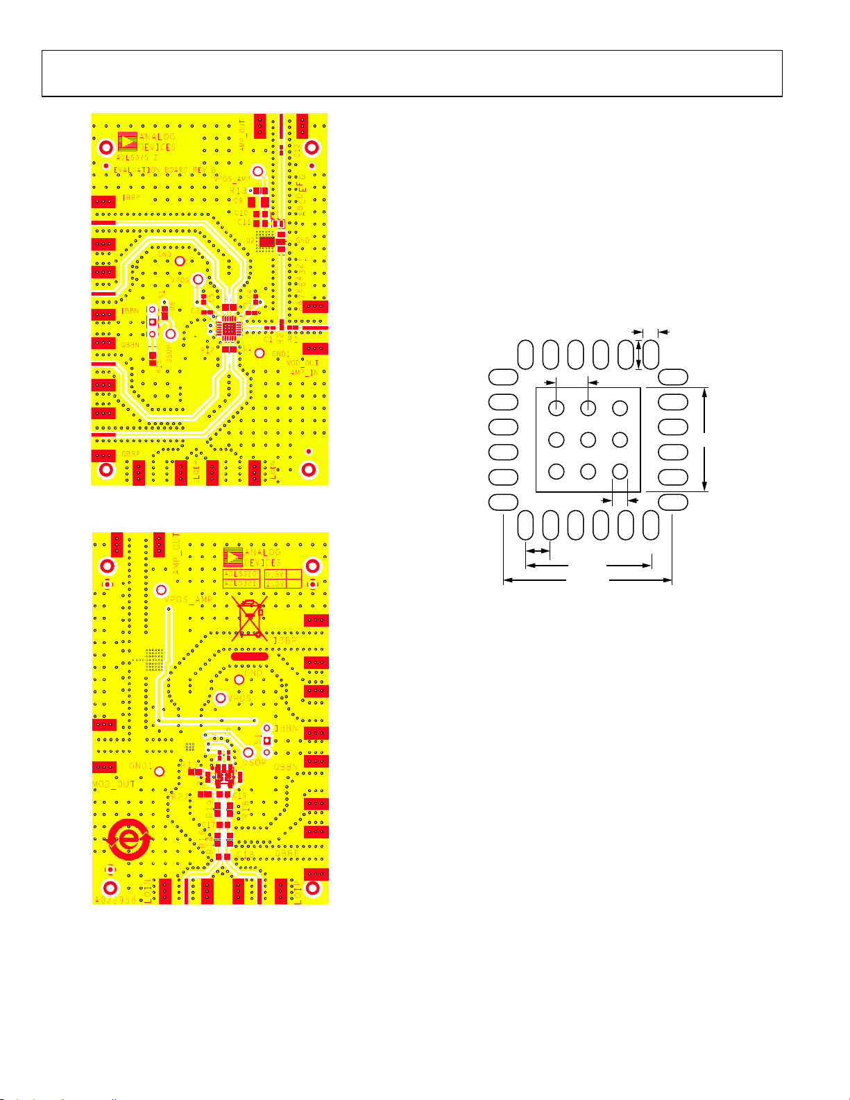
Data Sheet ADL5375
Thermal Grounding and Evaluation Board Layout
The package for the ADL5375 features an exposed paddle on
the underside that should be well soldered to a low thermal
and electrical impedance ground plane. This paddle is typically
soldered to an exposed opening in the solder mask on the
evaluation board. Figure 78 illustrates the dimensions used in
the layout of the ADL5375 footprint on the ADL5375 Evaluation
Board (1 mil. = 0.0254 mm).
Notice the use of nine via holes on the exposed paddle. These
ground vias should be connected to all other ground layers on
the evaluation board to maximize heat dissipation from the
device package.
12 mil.
23 mil.
82 mil.
Figure 76. Evaluation Board Layout, Top Layer
25 mil.
07052-127
12 mil.
19.7 mil.
98.4 mil.
133.8 mi l.
Figure 78. Dimensions for Evaluation Board Layout for the ADL5375 Package
07052-046
Under these conditions, the thermal impedance of the ADL5375
was measured to be approximately 30°C/W in still air.
Figure 77. Evaluation Board Layout, Bottom Layer
07052-128
Rev. B | Page 32 of 36
Data Sheet ADL5375
CHARACTERIZATION SETUP
AEROFLEX IFR 3416
250kHz TO 6GHz SIGNAL GENERATOR
FREQ 1MHz LEVEL 0dBm
BIAS 0.5V
BIAS 0.5V
AGILENT 34401A
MULTIMETER
0.194 ADC
VPOS +5V
AGILENT E3631A
POWER SUPPLY
5.000 0.194A
6V
+
GAIN 0.5V
GAIN 0.5V
CONNECT TO BACK OF UNIT
I/AM Q/FM
IOUT QOUT
90°
±25V
–
–
+
COM
IQ
Figure 79. Characterization Bench Setup
The primary setup used to characterize the ADL5375 is shown
in Figure 79. This setup was used to evaluate the product as a
single-sideband modulator. The aeroflex signal generator supplied
the LO and differential I and Q baseband signals to the device
under test (DUT). The typical LO drive was 0 dBm. The I-channel
is driven by a sine wave, and the Q-channel is driven by a cosine
wave. The lower sideband is the single-sideband (SSB) output.
ROHDE & SCHWARTZ
SPECTRUM ANALYZER
RF
OUT
IP
IN
QP
QN
LO
0°
MOD
LO
OUT
GNDVPOS
FSU 20Hz TO 8GHz
+6dBm
MOD TEST SETUP
OUTPUT
RF
IN
07052-049
The majority of characterization for the ADL5375 was performed
using a 1 MHz sine wave signal with a 500 mV (ADL5375-05)
or 1500 mV (ADL5375-15) common-mode voltage applied to
the baseband signals of the DUT. The baseband signal path was
calibrated to ensure that the V
and V
IOS
offsets on the baseband
QOS
inputs were minimized as close as possible to 0 V before
connecting to the DUT. See the Carrier Feedthrough Nulling
section for the definitions of V
IOS
and V
QOS
.
Rev. B | Page 33 of 36
ADL5375 Data Sheet
TEKTRONIX AFG3252
ARBITRARY FUNCTION GENERATOR
DUAL FUNCTION
1MHz
CH1
AMPL 500mV p-p
PHASE 0°
1MHz
CH2
AMPL 500mV p-p
PHASE 90°
AGILENT E3631A
POWER SUPPLY
5.000 0.350A
6V
VPOS +5V
0.500 0.010A
–
+
VPOS +5V
AGILENT E3631A
POWER SUPPLY
+
0°
+5V
±25V
COM
–
–5V
CH1 OUTPUT
CH2 OUTPUT
IQ
MOD TEST RACK
90°
SINGLE-TO-DIFFERENTIAL
CIRCUIT BOARD
Q IN AC
Q IN DCCM
TSEN GND
VPOSB VPOSA
IN1
AGND
VN1 VP1
I IN DCCM
I IN AC
250kHz TO 6G Hz SIGNAL GENERATOR
IN1
AEROFLEX IFR 3416
LEVEL 0dBm
IP
IN
QP
QN
MOD
CHAR BD
IP
IN
QP
QN
VPOS
ROHDE & SCHWARTZ
SPECTRUM ANALYZER
FSU 20Hz TO 8G Hz
LO
OUT
GND
RF
OUT
LO
OUTPUT
6V ±25V
–
+
VCM = 0.5V
AGILENT 34401A
MULTIMETER
0.200 ADC
–
+
COM
Figure 80. Setup for Baseband Frequency Sweep and Undesired Sideband Nulling
The setup used to evaluate baseband frequency sweep and
undesired sideband nulling of the ADL5375 is shown in Figure 80.
The interface board has circuitry that converts the single-ended
I input and Q input from the arbitrary function generator to
differential I and Q baseband signals with a dc bias of 500 mV
RF
IN
07052-050
(ADL5375-05) or 1500 mV (ADL5375-15). Undesired sideband
nulling was achieved through an iterative process of adjusting
amplitude and phase on the Q-channel. See Sideband
Suppression Optimization section for a detailed description on
sideband nulling.
Rev. B | Page 34 of 36
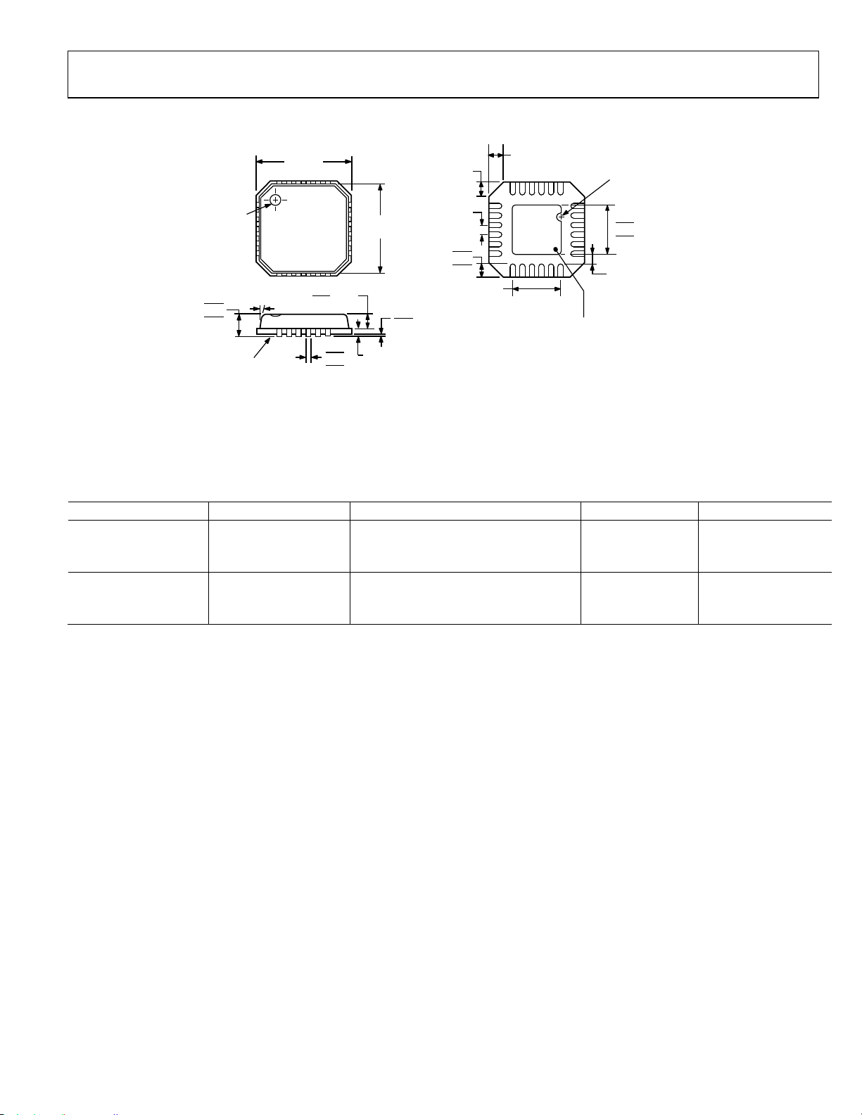
Data Sheet ADL5375
OUTLINE DIMENSIONS
0.60 MAX
PIN 1
INDICATOR
1
19
18
(BOTTOMVIEW)
13
12
24
EXPOSED
PA D
6
7
FOR PROPER CONNECTION OF
THE EXPOSED PAD, REFER TO
THE PIN CONFIGURATION AND
FUNCTION DESCRIPTIONS
SECTION OF THIS DATA SHEET.
2.65
2.50 SQ
2.35
0.23 MIN
082908-A
PIN 1
INDICATOR
1.00
0.85
0.80
SEATING
PLANE
12° MAX
4.00
BSC SQ
TOP
VIEW
0.80 MAX
0.65 TYP
0.30
0.23
0.18
COMPLIANT TO JEDEC STANDARDS MO-220-VGGD-8
3.75
BSC SQ
0.20 REF
0.60 MAX
0.05 MAX
0.02 NOM
COPLANARITY
BSC
0.08
0.50
0.50
0.40
0.30
2.50 REF
Figure 81. 24-Lead Lead Frame Chip Scale Package [LFCSP_VQ]
4 mm × 4 mm Body, Very Thin Quad
(CP-24-3)
Dimensions shown in millimeters
ORDERING GUIDE
Model1 Temperature Range Package Description Package Option Ordering Quantity
ADL5375-05ACPZ-R7 −40°C to +85°C 24-Lead LFCSP_VQ, 7” Tape and Reel CP-24-3 1,500
ADL5375-05ACPZ-WP −40°C to +85°C 24-Lead LFCSP_VQ, Waffle Pack CP-24-3 64
ADL5375-05-EVALZ Evaluation Board
ADL5375-15ACPZ-R7 −40°C to +85°C 24-Lead LFCSP_VQ, 7” Tape and Reel CP-24-3 1,500
ADL5375-15ACPZ-WP −40°C to +85°C 24-Lead LFCSP_VQ, Waffle Pack CP-24-3 64
ADL5375-15-EVALZ Evaluation Board
1
Z = RoHS Compliant Part.
Rev. B | Page 35 of 36

ADL5375 Data Sheet
NOTES
©2007–2011 Analog Devices, Inc. All rights reserved. Trademarks and
registered trademarks are the property of their respective owners.
D07052-0-9/11(B)
Rev. B | Page 36 of 36
 Loading...