500 MHz to 1500 MHz
FEATURES
Output frequency range: 500 MHz to 1500 MHz
Modulation bandwidth: >500 MHz (3 dB)
1 dB output compression: 14.4 dBm @ 900 MHz
Noise floor: −158.6 dBm/Hz @ 915 MHz
Sideband suppression: −55 dBc @ 900 MHz
Carrier feedthrough: −50 dBm @ 900 MHz
Single supply: 4.75 V to 5.25 V
24-lead LFCSP
APPLICATIONS
Cellular communication systems at 900 MHz
CDMA2000/GSM
WiMAX/broadband wireless access systems
Cable communication equipment
Satellite modems
GENERAL DESCRIPTION
The ADL5371 is a member of the fixed-gain quadrature modulator
(F-MOD) family designed for use from 500 MHz to 1500 MHz.
Its excellent phase accuracy and amplitude balance enable high
performance intermediate frequency or direct radio frequency
modulation for communication systems.
The ADL5371 provides a >500 MHz, 3 dB baseband bandwidth,
making it ideally suited for use in broadband zero IF or low IFto-RF applications and in broadband digital predistortion
transmitters.
Quadrature Modulator
ADL5371
FUNCTIONAL BLOCK DIAGRAM
IBBP
IBBN
LOIP
LOIN
QBBN
QBBP
The ADL5371 accepts two differential baseband inputs and
a single-ended local oscillator (LO) and generates a singleended output.
The ADL5371 is fabricated using the Analog Devices, Inc.
advanced silicon-germanium bipolar process. It is available in a
24-lead, exposed-paddle, Pb-free, LFCSP. Performance is specified
over a −40°C to +85°C temperature range. A Pb-free evaluation
board is available.
QUADRATURE
PHASE
SPLITTER
Figure 1.
VOUT
06510-001
Rev. 0
Information furnished by Analog Devices is believed to be accurate and reliable. However, no
responsibility is assumed by Anal og Devices for its use, nor for any infringements of patents or ot her
rights of third parties that may result from its use. Specifications subject to change without notice. No
license is granted by implication or otherwise under any patent or patent rights of Analog Devices.
Trademarks and registered trademarks are the property of their respective owners.
One Technology Way, P.O. Box 9106, Norwood, MA 02062-9106, U.S.A.
Tel: 781.329.4700 www.analog.com
Fax: 781.461.3113 ©2007 Analog Devices, Inc. All rights reserved.

ADL5371
TABLE OF CONTENTS
Features.............................................................................................. 1
Applications....................................................................................... 1
Functional Block Diagram .............................................................. 1
General Description ......................................................................... 1
Revision History ............................................................................... 2
Specifications..................................................................................... 3
Absolute Maximum Ratings............................................................ 4
ESD Caution.................................................................................. 4
Pin Configuration and Function Descriptions............................. 5
Typical Performance Characteristics ............................................. 6
Theory of Operation ...................................................................... 10
Circuit Description..................................................................... 10
Basic Connections ..........................................................................11
Power Supply and Grounding................................................... 11
Baseband Inputs.......................................................................... 11
LO Input ...................................................................................... 11
RF Output.................................................................................... 11
Optimization............................................................................... 12
Applications Information.............................................................. 13
DAC Modulator Interfacing ..................................................... 13
Limiting the AC Swing .............................................................. 13
Filtering........................................................................................ 13
Using the AD9779 Auxiliary DAC for Carrier Feedthrough
Nulling ......................................................................................... 14
GSM Operation .......................................................................... 14
LO Generation Using PLLs....................................................... 15
Transmit DAC Options ............................................................. 15
Modulator/Demodulator Options ........................................... 15
Evaluation Board............................................................................ 16
Characterization Setup .................................................................. 17
Outline Dimensions....................................................................... 19
Ordering Guide .......................................................................... 19
REVISION HISTORY
1/07—Revision 0: Initial Version
Rev. 0 | Page 2 of 20

ADL5371
SPECIFICATIONS
VS = 5 V; TA = 25°C; LO = 0 dBm1 single-ended; baseband I/Q amplitude = 1.4 V p-p differential sine waves in quadrature with a 500 mV
dc bias; baseband I/Q frequency (f
Table 1.
Parameter Conditions Min Typ Max Unit
ADL5371 Low frequency 500 MHz
High frequency 1500 MHz
Output Power, P
OUT
Output P1dB 14.4 dBm
Carrier Feedthrough −50 dBm
Sideband Suppression −55 dBc
Quadrature Error 0.1 Degrees
I/Q Amplitude Balance −0.03 dB
Second Harmonic P
Third Harmonic P
Output IP2 f1BB = 3.5 MHz, f2BB = 4.5 MHz, P
Output IP3 f1BB = 3.5 MHz, f2BB = 4.5 MHz, P
Noise Floor
GSM 6 MHz carrier offset, P
LO INPUTS
LO Drive Level
1
Input Return Loss See Figure 9 for the return loss vs. frequency plot −7 dB
BASEBAND INPUTS Pin IBBP, Pin IBBN, Pin QBBP, Pin QBBN
I/Q Input Bias Level 500 mV
Input Bias Current Current sourcing from each baseband input with a bias of 500 mV dc
Input Offset Current 0.1 μA
Differential Input Impedance 2900 kΩ
Bandwidth (0.1 dB) 70 MHz
Bandwidth (1 dB) 350 MHz
POWER SUPPLIES Pin VPS1, Pin VPS2, Pin VPS3, Pin VPS4, and Pin VPS5
Voltage 4.75 5.25 V
Supply Current 175 200 mA
1
Higher LO drive reduces noise at a 6 MHz carrier offset in GSM applications.
2
See the V-to-I Converter section for architecture information.
) = 1 MHz, LO frequency = 900 MHz, unless otherwise noted.
BB
7.6 dBm
− (fLO + (2 × fBB)), P
OUT
− (fLO + (3 × fBB)), P
OUT
I/Q inputs = 0 V differential with a 500 mV common-mode bias,
= 6.2 dBm −56 dBc
OUT
= 6.2 dBm −50 dBc
OUT
= 1.6 dBm per tone 57 dBm
OUT
= 1.6 dBm per tone 27 dBm
OUT
−158.6 dBm/Hz
20 MHz carrier offset
= 5 dBm, PLO = 6 dBm, LO = 940 MHz −158.5 dBc/Hz
OUT
Characterization performed at typical level −6 0 +6 dBm
2
45 μA
Rev. 0 | Page 3 of 20

ADL5371
ABSOLUTE MAXIMUM RATINGS
Table 2.
Parameter Rating
Supply Voltage VPOS 5.5 V
IBBP, IBBN, QBBP, QBBN 0 V to 2 V
LOIP and LOIN 13 dBm
Internal Power Dissipation 1188 mW
θJA (Exposed Paddle Soldered Down) 54°C/W
Maximum Junction Temperature 152°C
Operating Temperature Range −40°C to +85°C
Storage Temperature Range −65°C to +150°C
Stresses above those listed under Absolute Maximum Ratings
may cause permanent damage to the device. This is a stress
rating only; functional operation of the device at these or any
other conditions above those indicated in the operational
section of this specification is not implied. Exposure to absolute
maximum rating conditions for extended periods may affect
device reliability.
ESD CAUTION
Rev. 0 | Page 4 of 20

ADL5371
PIN CONFIGURATION AND FUNCTION DESCRIPTIONS
QBBP
COM4
QBBN
COM4
IBBN
IBBP
2422232120
19
COM1
COM1
VPS1
VPS1
VPS1
VPS1
1
2
3
4
5
6
F-MOD
TOP VIEW
(Not to Scale)
798
101112
LOIP
LOIN
COM2
COM2
COM3
VPS5
18
VPS4
17
VPS3
16
VPS2
15
VPS2
14
VOUT
13
COM3
06510-002
Figure 2. Pin Configuration
Table 3. Pin Function Descriptions
Pin No. Mnemonic Description
1, 2 COM1 Input Common Pins. Connect to ground plane via a low impedance path.
7, 10 COM2 Input Common Pins. Connect to ground plane via a low impedance path.
11, 12 COM3 Input Common Pins. Connect to ground plane via a low impedance path.
21, 22 COM4 Input Common Pins. Connect to ground plane via a low impedance path.
3 to 6 VPS1
Positive Supply Voltage Pins. All pins should be connected to the same supply (V
adequate external bypassing, connect 0.1 μF capacitors between each pin and ground.
Adjacent power supply pins of the same name can share one capacitor (see Figure 23).
14, 15 VPS2
Positive Supply Voltage Pins. All pins should be connected to the same supply (V
adequate external bypassing, connect 0.1 μF capacitors between each pin and ground.
Adjacent power supply pins of the same name can share one capacitor (see Figure 23).
16 to 18 VPS3 to VPS5
Positive Supply Voltage Pins. All pins should be connected to the same supply (V
adequate external bypassing, connect 0.1 μF capacitors between each pin and ground.
Adjacent power supply pins of the same name can share one capacitor (see Figure 23).
8, 9 LOIP, LOIN
50 Ω Single-Ended Local Oscillator Input. Internally dc-biased. Pins must be ac-coupled.
AC-couple LOIN to ground and drive LO through LOIP.
13 VOUT
Device Output. Single-ended RF output. Pin should be ac-coupled to the load. The output is
ground referenced.
19, 20, 23, 24
IBBP, IBBN,
QBBN, QBBP
Differential In-Phase and Quadrature Baseband Inputs. These high impedance inputs must be
dc-biased to 500 mV dc and must be driven from a low impedance source. Nominal characterized
ac signal swing is 700 mV p-p on each pin. This results in a differential drive of 1.4 V p-p with a
500 mV dc bias. These inputs are not self-biased and must be externally biased.
Exposed Paddle Connect to ground plane via a low impedance path.
). To ensure
S
). To ensure
S
). To ensure
S
Rev. 0 | Page 5 of 20

ADL5371
TYPICAL PERFORMANCE CHARACTERISTICS
VS = 5 V; TA = 25°C; LO = 0 dBm single-ended; baseband I/Q amplitude = 1.4 V p-p differential sine waves in quadrature with a 500 mV
dc bias; baseband I/Q frequency (f
10
9
8
7
6
5
4
3
SSB OUTPUT P OWER (dBm)
2
1
0
10
9
8
7
6
5
4
3
SSB OUTPUT POWER (dBm)
2
1
0
TA = –40°C
500 600 700 800 900 1000 1100 1200 1300 1400 1500
LO FREQUENCY (MHz)
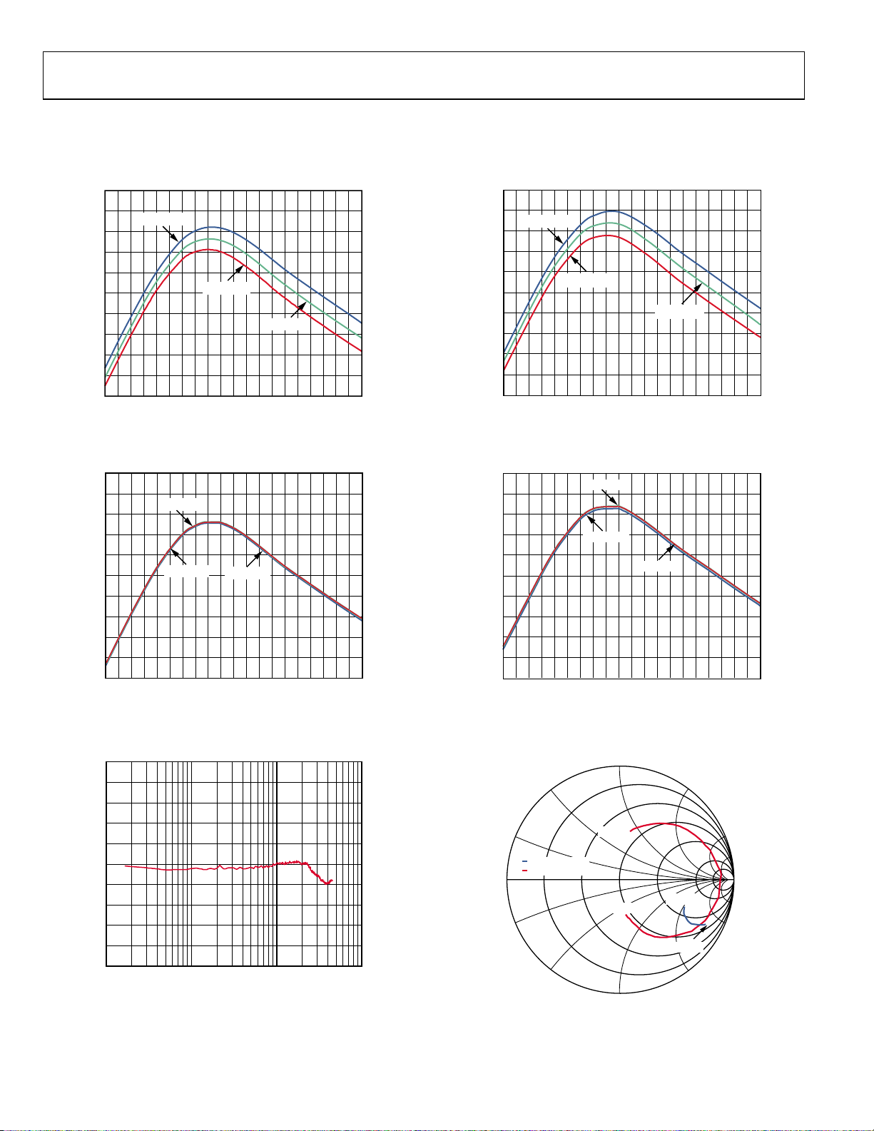
Figure 3. Single Sideband (SSB) Output Power (P
LO Frequency (f
VS = 5.0V
VS = 4.75V
500 600 700 800 900 1000 1100 1200 1300 1400 1500
LO FREQUENCY (MHz)
Figure 4. Single Sideband (SSB) Output Power (P
LO Frequency (f
5
) = 1 MHz, unless otherwise noted.
BB
TA = +85°C
TA = +25°C
) vs.
) and Temperature
LO
VS = 5.25V
) and Supply
LO
OUT
OUT
) vs.
16
15
TA = –40°C
14
13
12
11
10
9
8
1dB OUTPUT COMPRESSI ON (dBm)
7
6
500 600 700 800 900 1000 1100 1200 1300 1400 1500
6510-003
Figure 6. SSB Output 1 dB Compression Point (OP1dB) vs. f
16
15
14
13
12
11
10
9
8
1dB OUTPUT COMPRESSI ON (dBm)
7
6
500 600 700 800 900 1000 1100 1200 1300 1400 150 0
6510-004
Figure 7. SSB Output 1 dB Compression Point (OP1dB) vs. f
120
TA = +85°C
LO FREQ UENCY (MHz)
VS = 5.0V
VS = 5.25V
LO FREQ UENCY (MHz)
90
TA = +25°C
VS = 4.75V
and Temperature
LO
and Supply
LO
60
06510-006
06510-007
0
OUTPUT PO WER VARIANCE (d B)
–5
1 10 100 1000
BASEBAND FREQUENCY (M Hz)
Figure 5. I/Q Input Bandwidth Normalized to
Gain @ 1 MHz (f
= 900 MHz)
LO
06510-005
Rev. 0 | Page 6 of 20
150
210
S11 OF LOIP
S22 OF OUTPUT
240
500MHz
1500MHz
1500MHz
500MHz
270
Figure 8. Smith Chart of LOIP S11 and VOUT S22
from 500 MHz to 1500 MHz)
(f
LO
300
30
330
0180
06510-008
 Loading...