Cascadable IF VGAs with
A
FEATURES
Pair of VGAs with rms AGC detectors
VGA and AGC modes of operation
Continuous gain control range: 48 dB
Noise figure (NF) = 6.8 dB at maximum gain
IMD3 > 62 dBc for 1.0 V p-p composite output
Differential input and output
Multiplexed inputs for VGA2
Programmable detector AGC setpoints
Programmable VGA maximum gain
Power-down feature
Single 5 V supply operation
APPLICATIONS
Point-to-multipoint radios
Instrumentation
Medical
Programmable RMS Detectors
ADL5336
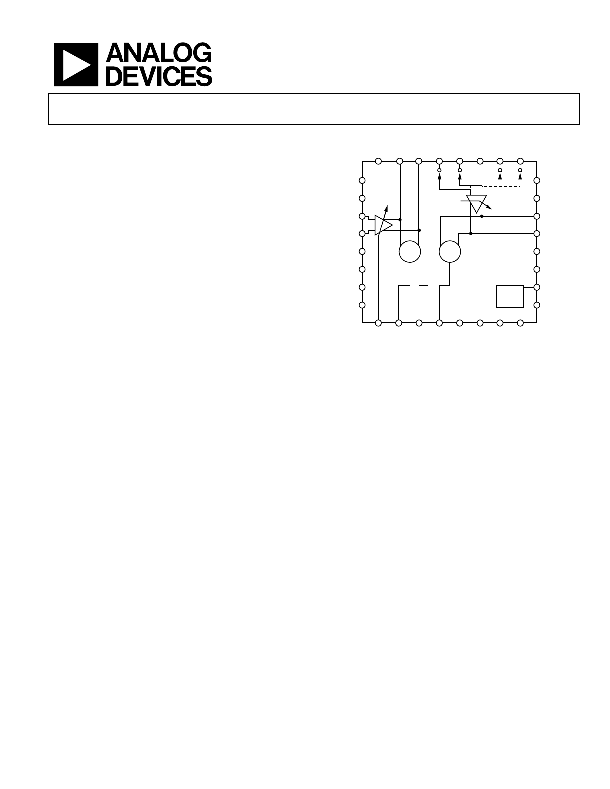
FUNCTIONAL BLOCK DIAGRAM
COM
VCM1
VPOS
INP1
INM1
VPOS
COM
MODE
ENBL
OPP1 OPM1 IP2
VGA1
2
X
GAIN1 DT O1 GAI N2 DTO2 COMD VPSD LE CLK
IM2ACOM IP2B IM2B
2
X
Figure 1.
ADL5336
VGA2
VCM2
VPOS
OPP2
OPM2
VPOS
COM
SDO
SPI
DATA
09550-001
GENERAL DESCRIPTION
The ADL5336 consists of a pair of variable gain amplifiers
(VGAs) designed for cascaded IF applications. The amplifiers
have linear-in-dB gain control and operate from low frequencies to
1 GHz. Their excellent gain conformance over the control range
and flatness over frequency are due to Analog Devices, Inc.,
patented X-AMP® architecture, an innovative technique for
implementing high performance variable gain control.
Each VGA has 24 dB of gain control range. Their maximum gain
can be independently programmable over a 6 dB range via the
SPI. The VGAs can be cascaded to provide a total range of 48 dB.
When connected to a 50 source through a 1:4 balun, the gain
is 6 dB higher. The second VGA has an SPI programmable input
switch that selects one of two external inputs.
When driven from a 200 Ω source or from a 50 Ω source through
a 1:4 balun, the noise figure (NF) for the composite amplifier is
6.8 dB at maximum gain. The output of each VGA can drive
100 Ω loads to 5 V p-p maximum.
Each VGA has an independent square law detector for autonomous,
automatic gain control (AGC) operation. Each detector setpoint
can be programmed independently through the SPI from −24 dBV
to −3 dBV in 3 dB steps. When both VGAs are arranged in AGC
mode and are programmed to the same setpoint, the composite NF
increases to 9 dB when backed off by 18 dB from maximum gain.
The ADL5336 operates from a 5 V supply and consumes a typical
supply current of 80 mA. When disabled, it consumes 4 mA. It is
fabricated in an advanced silicon-germanium BiCMOS process and
is available in a 32-lead exposed paddle LFCSP package. Performance
is specified over a −40°C to +85°C temperature range.
Rev. A
Information furnished by Analog Devices is believed to be accurate and reliable. However, no
responsibility is assumed by Analog Devices for its use, nor for any infringements of patents or other
rights of third parties that may result from its use. Specifications subject to change without notice. No
license is granted by implication or otherwise under any patent or patent rights of Analog Devices.
Trademarks and registered trademarks are the property of their respective owners.
One Technology Way, P.O. Box 9106, Norwood, MA 02062-9106, U.S.A.
Tel: 781.329.4700 www.analog.com
Fax: 781.461.3113 ©2011 Analog Devices, Inc. All rights reserved.

ADL5336
TABLE OF CONTENTS
Features.............................................................................................. 1
Applications....................................................................................... 1
Functional Block Diagram ..............................................................1
General Description......................................................................... 1
Revision History ...............................................................................2
Specifications..................................................................................... 3
Timing Diagrams.......................................................................... 5
Absolute Maximum Ratings............................................................ 6
ESD Caution.................................................................................. 6
Pin Configuration and Function Descriptions............................. 7
Typical Performance Characteristics............................................. 8
Theory of Operation ......................................................................17
Circuit Description.....................................................................17
Gain Control Interface............................................................... 18
Input and Output Impedances..................................................18
AGC Operation........................................................................... 18
Register Map and Codes................................................................ 19
Applications Information.............................................................. 20
Basic Connections...................................................................... 20
Supply Decoupling..................................................................... 20
Input Signal Path........................................................................ 20
Output Signal Path..................................................................... 20
Detector Output and Gain Pin................................................. 21
Common-Mode Bypassing....................................................... 21
Serial Port Connections............................................................. 21
Mode and Enable Connections................................................ 21
Error Vector Magnitude (EVM)............................................... 21
Effect of C
AGC Insensitivity to Modulation Type................................... 22
Effect of Setpoint on EVM........................................................ 23
Cascaded VGA/AGC Performance.......................................... 23
Evaluation Board Layout............................................................... 25
Bill of Materials (BOM)............................................................. 27
Evaluation Board Control Software......................................... 28
Outline Dimensions....................................................................... 29
Ordering Guide .......................................................................... 29
on EVM............................................................... 22
AGC
REVISION HISTORY
6/11—Rev. 0 to Rev. A
Changes to Table 1............................................................................ 3
Changes to Typical Performance Charteristics
Section Format.................................................................................. 8
Changes to Figure 7 and Figure 10................................................. 8
Changes to Figure 11 to Figure 16.................................................. 9
Changes to Figure 17 to Figure 22................................................ 10
Changes to Figure 23 and Figure 26............................................. 11
Inserted Figure 53 and Figure 56; Renumbered Sequentially... 16
Changes to Figure 60...................................................................... 17
Changes to Figure 61 Caption....................................................... 18
Changes to Cascaded VGA/AGC Performance Section and
Figure 68 ..........................................................................................24
Changes to Figure 72...................................................................... 26
2/11—Revision 0: Initial Version
Rev. A | Page 2 of 32

ADL5336
SPECIFICATIONS
VS = 5 V, TA = 25°C, ZS = 200 Ω, Z
unless otherwise noted. 1:4 balun voltage gain is not included. All dBm numbers are with respect to each VGA’s load impedance.
Table 1.
Parameter Test Conditions/Comments Min Typ Max Unit
OVERALL FUNCTION
Frequency Range
Maximum Input INP1/INM1, IP2A/IM2A, IP2B/IM2B differential 8 V p-p
Maximum Output OPP1/OPM1, OPP2/OPM2 differential at P1dB 5 V p-p
AC Input Impedance
VGA1 Differential across INP1, INM1 200 Ω
VGA2 Selected Input Differential across IP2A, IM2A or IP2B, IM2B 200 Ω
VGA2 Unselected Input 10 kΩ
AC Output Impedance VGA1 1 Ω
VGA2 3.5 Ω
GAIN CONTROL INTERFACE GAIN1/GAIN2, MODE
Voltage Gain Range GAIN1/GAIN2 from 0 V to 1 V
VGA1 Gain Code 00 −14.6 +9.7 dB
Gain Code 01 −12.2 +12 dB
Gain Code 10 −10.3 +13.8 dB
Gain Code 11 −8.9 +15.2 dB
VGA2 Gain Code 00 −10.8 +13.4 dB
Gain Code 01 −8.2 +15.9 dB
Gain Code 10 −6.6 +17.7 dB
Gain Code 11 −4.7 +19.5 dB
Gain Step Response Time 8.5 dB Gain Step 5 ns
Gain Slope
VGA1 MODE = VS 35 mV/dB
VGA2 35 mV/dB
Gain Error V
Input Impedance V
f = 140 MHz
Noise Figure VGA1, Gain Code 00, V
VGA2, Gain Code 11, V
Output IP3 VGA1, Gain Code 00, V
Output Voltage Level of 1.0 V p-p
VGA1, Gain Code 11, V
VGA2, Gain Code 00, V
VGA2, Gain Code 11, V
Output P1dB VGA1, Gain Code 00, V
VGA1, Gain Code 11, V
VGA2, Gain Code 00, V
VGA2, Gain Code 11, V
L VGA1
= 200 Ω, Z
= 100 Ω, RF input = −20 dBm at 140 MHz, maximum gain setting for both VGAs,
L VGA2
3 dB bandwidth LF 1000 MHz
from 0.2 V to 0.8 V ±0.2 dB
GAINx
to COM 4.6 MΩ
GAINx
= 1 V 7.4 dB
GAIN
= 1 V 7.1 dB
GAIN
= 1 V 21 (28) dBV (dBm)
GAIN
= 1 V 18 (25) dBV (dBm)
GAIN
= 1 V 26 (36) dBV (dBm)
GAIN
= 1 V 24 (34) dBV (dBm)
GAIN
= 1 V 3.5(10.5) dBV (dBm)
GAIN
= 1 V 3.5(10.5) dBV (dBm)
GAIN
= 1 V 4 (14) dBV (dBm)
GAIN
= 1 V 4 (14) dBV (dBm)
GAIN
Rev. A | Page 3 of 32

ADL5336
Parameter Test Conditions/Comments Min Typ Max Unit
f = 350 MHz
Noise Figure VGA1, Gain Code 00, V
VGA2, Gain Code 11, V
Output IP3 VGA1, Gain Code 00, V
Output Voltage Level of 1.0 V p-p VGA1, Gain Code 11, V
VGA2, Gain Code 00, V
VGA2, Gain Code 11, V
Output P1dB VGA1, Gain Code 00, V
VGA1, Gain Code 11, V
VGA2, Gain Code 00, V
VGA2, Gain Code 11, V
SQUARE LAW DETECTORS DTO1, DTO2
Output Setpoint SPI controlled, 3 dB steps −24 −3 dBV
Output Range 0.1 VS/2 V
AGC Step Response Range 5 dB input step, C
DIGITAL LOGIC LE, CLK, DATA, SDO
Input High Voltage, V
Input Low Voltage, V
Input Current, I
INH/IINL
>2.2 V
INH
<1.8 V
INL
<1 µA
Input Capacitance, CIN 2 pF
SPI TIMING LE, CLK, DATA, SDO
f
20 MHz
CLK
tDH DATA hold time 5 ns
tDS DATA setup time 5 ns
tLH LE hold time 5 ns
tLS LE setup time 5 ns
tPW CLK high pulse width 5 ns
tD CLK-to-SDO delay 5 ns
POWER AND ENABLE VPOS, VPSD, COM, COMD, ENBL
Supply Voltage Range 4.5 5 5.5 V
Total Supply Current ENBL = 5 V 80 mA
Disable Current ENBL = 0 V 4 mA
Disable Threshold 2.3 V
Enable Response Time
Delay following low-to-high transition until
device meets full specifications in VGA mode
Disable Response Time
Delay following high-to-low transition until
device produces full attenuation in VGA mode
= 1 V 8 dB
GAIN
= 1 V 7.7 dB
GAIN
= 1 V 12 (19) dBV (dBm)
GAIN
= 1 V 10.5(17.5) dBV (dBm)
GAIN
= 1 V 18 (28) dBV (dBm)
GAIN
= 1 V 16 (26) dBV (dBm)
GAIN
= 1 V 0 (7) dBV (dBm)
GAIN
= 1 V 0 (7) dBV (dBm)
GAIN
= 1 V −1.5 (+8.5) dBV (dBm)
GAIN
= 1 V −1.5 (+8.5) dBV (dBm)
GAIN
= 0.1 µF 1.5 ms
AGC
800 ns
20 ns
Rev. A | Page 4 of 32
ADL5336
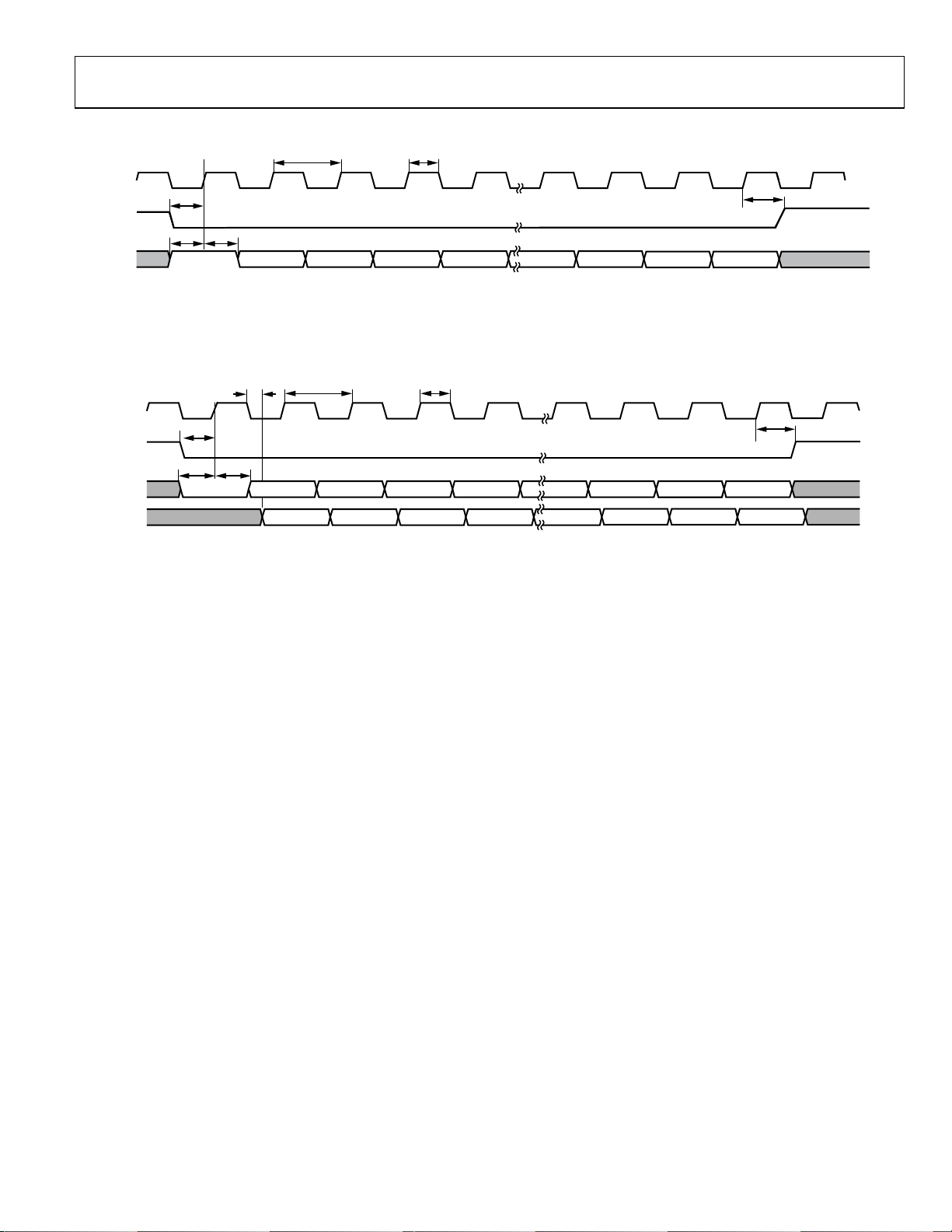
TIMING DIAGRAMS
t
CLK
CLK
LE
DATA
NOTES
1. THE FIRST DATA BIT DETERMINES WHETHER THE PART IS WRITING TO OR READING FROM THE INTERNAL 8-BIT REGISTER. FOR A WRITE
OPERATION, THE FIRST BIT SHOULD BE A LOGIC 1. THE 8-BIT WORD IS THEN REGISTERED INTO THE DATA PIN ON CONSECUTIVE RISING
EDGES OF THE CLOCK.
t
LS
t
t
DS
WRITE BIT
DH
LSB + 1LSB
t
CLK
DCDCREAD BIT DC DC DC DC DC
CLK
DATA
t
D
t
LS
LE
t
t
DH
DS
t
PW
LSB + 2
LSB + 3 MSB – 3 MSB – 2
Figure 2. Write Mode Timing Diagram
t
PW
MSB – 1 MSB
t
LH
09550-002
t
LH
DCDC
SDO
NOTES
1. THE FI RST DATA BIT DETERMINES WHETHER THE PART IS W RITING T O OR READING FROM THE INTERNAL 8- BIT REGI STER. F OR A READ
OPERATIO N, THE FI RST BIT SHOULD BE A LO GIC 0. T HE 8-BIT WO RD IS THEN UPDATED AT THE SDO PIN ON CONSECUTIVE F ALLING EDGES
OF THE CLOCK.
LSB + 1LSB
LSB + 2
LSB + 3 MSB – 3
MSB – 2
MSB – 1 MSB
Figure 3. Read Mode Timing Diagram
09550-003
Rev. A | Page 5 of 32
ADL5336
ABSOLUTE MAXIMUM RATINGS
Table 2.
Parameter Rating
Supply Voltages (VPOS, VPSD) 5.5 V
LE, CLK, DATA, SDO VPOS + 0.5 V
ENBL, MODE VPOS + 0.5 V
INP1, INM1, IP2A, IM2A, IP2B, IM2B VPOS + 0.5 V
OPP1, OPM1, OPP2, OPM2 VPOS + 0.5 V
DTO1, DTO2, GAIN1, GAIN2 VPOS/2 + 0.5 V
Internal Power Dissipation 530 mW
θJA (With Pad Soldered to Board) 37.4°C/W
Maximum Junction Temperature 150°C
Operating Temperature Range −40°C to +85°C
Storage Temperature Range −65°C to +150°C
Lead Temperature (Soldering, 60 sec) 300°C
Stresses above those listed under Absolute Maximum Ratings
may cause permanent damage to the device. This is a stress
rating only; functional operation of the device at these or any
other conditions above those indicated in the operational
section of this specification is not implied. Exposure to absolute
maximum rating conditions for extended periods may affect
device reliability.
ESD CAUTION
Rev. A | Page 6 of 32

ADL5336
PIN CONFIGURATION AND FUNCTION DESCRIPTIONS
1
IM2B
IP2B
COM
IM2A
IP2A
OPM
OPP1
COM
25
26
27
28
29
30
31
32
1VCM1
PIN 1
2VPOS
INDICATOR
3INP1
4INM1
ADL5336
5VPOS
6COM
TOP VIEW
7MODE
(Not to Scale)
8ENBL
9
11
13
12
10
O2
DT
DTO1
COMD
GAIN2
GAIN1
NOTES
1. EXPOS ED PADDLE. CONNECT TO LOW
IMPEDANCE G ROUND PAD.
24 VCM 2
23 VPOS
22 OPP2
21 OPM2
20 VPOS
19 COM
18 SDO
17 DATA
16
15
14
LE
CLK
VPSD
09550-004
Figure 4. Pin Configuration
Table 3. Pin Function Descriptions
Pin No. Mnemonic Description
1, 24 VCM1, VCM2 Common-Mode Voltages. Decouple to common for ac-coupled operation.
2, 5, 14, 20, 23 VPOS, VPSD Analog and Digital Positive Supply Voltage (4.5 V to 5.5 V).
3, 4, 25, 26, 28, 29
INP1, INM1, IM2B,
Differential Inputs. 200 Ω input impedance; ac coupling recommended.
IP2B, IM2A, IP2A
6, 13, 19, 27, 32 COM, COMD Analog and Digital Common. Connect via lowest possible impedance to external circuit common.
7 MODE Gain Mode Control. Pull high for VGA mode, and pull low for AGC mode.
8 ENBL Chip Enable. Pull high to enable.
9, 11 GAIN1, GAIN2 Analog Gain Control (0 V to 1 V).
10, 12 DTO1, DTO2 Detector Outputs (0.1 V to VPOS/2 Range).
15, 16, 17, 18 LE, CLK, DATA, SDO SPI Programming and Data Readout Pins. CMOS levels V
21, 22, 30, 31
OPM2, OPP2,
Differential Outputs. Low output impedance; ac coupling recommended.
< 1.8 V, V
LOW
HIGH
> 2.2 V.
OPM1, OPP1
EP Exposed Paddle. Connect to low impedance ground pad.
Rev. A | Page 7 of 32
ADL5336
T
TYPICAL PERFORMANCE CHARACTERISTICS
VS = 5 V, TA = 25°C, ZS = 200 Ω, Z
11, V
= 1 V, setpoint code = 000, MODE = 5 V (VGA mode) for both amplifiers, unless otherwise noted.
GAIN
20
L VGA1
= 200 Ω, Z
= 100 Ω, RF input = −20 dBm at 140 MHz, unless otherwise noted. Gain code =
L VGA2
30
10
0
–10
GAIN1
–20
VOLTAGE GAIN (dB)
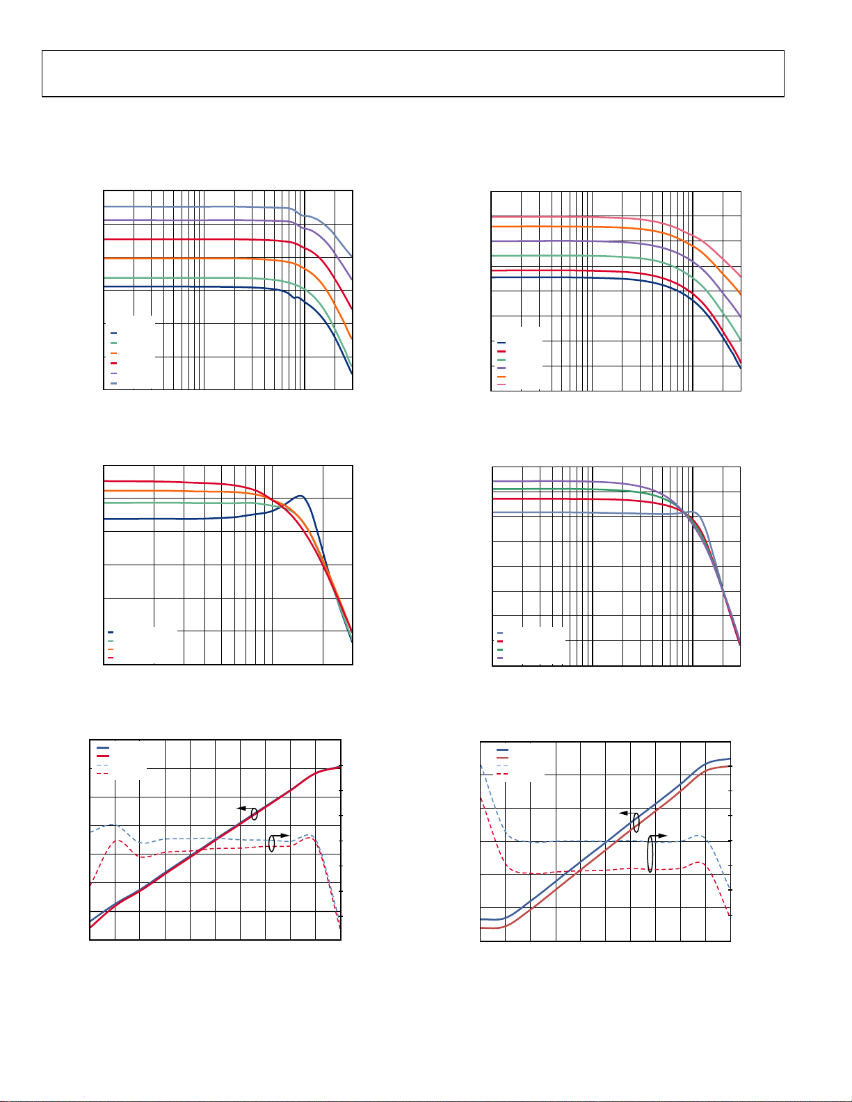
Figure 5. Gain vs. Frequency over V
0mV
200mV
400mV
–30
600mV
800mV
1000mV
–40
10M 100M 1G
FREQUENCY ( Hz)
at Gain Code 11 for VGA1
GAIN
5
0
–5
–10
–15
VOLTAGE GAIN (dB)
–20
GAIN CODE 00
GAIN CODE 01
GAIN CODE 10
GAIN CODE 11
–25
100M 1G
FREQUENCY ( Hz)
Figure 6. Gain vs. Frequency over Gain Code at V
20
140MHz
350MHz
140MHz
15
350MHz
10
5
0
VOLTAGE GAIN (dB)
–5
–10
= 0.5 V for VGA1
GAIN
2.0
1.5
1.0
0.5
0
–0.5
–1.0
–1.5
20
10
0
–10
AGE GAIN ( dB)
–20
VOL
GAIN2
–30
0mV
200mV
400mV
–40
600mV
800mV
1000mV
–50
10M 100M 1G
09550-005
Figure 8. Gain vs. Frequency over V
FREQUENC Y (Hz)
at Gain Code 11 for VGA2
GAIN
09550-008
10
5
0
–5
–10
–15
VOLTAGE GAIN (dB)
–20
GAIN CODE 00
GAIN CODE 01
–25
GAIN CODE 10
GAIN CODE 11
–30
10M 100M 1G
09550-006
Figure 9. Gain vs. Frequency over Gain Code at V
FREQUENCY ( Hz)
= 0.5 V for VGA2
GAIN
09550-009
25
20
15
10
ERROR (dB)
VOLTAGE GAIN (dB)
140MHz
350MHz
140MHz
350MHz
5
0
4
3
2
1
0
ERROR (dB)
–1
–2
–3
–15
0 100 200 300 400 500 600 700 800 900 1000
GAIN1 (mV)
Figure 7. Gain vs. V
over Frequency at Gain Code 11 for VGA1
GAIN
–2.0
–5
0 100 200 300 400 500 600 700 800 900 1000
09550-007
Figure 10. Gain vs. V
GAIN1 (mV)
over Frequency at Gain Code 11 for VGA2
GAIN
–4
09550-010
Rev. A | Page 8 of 32
ADL5336
T
m
T
20
4
25
4
15
10
5
0
AGE GAIN (dB)
VOL
–5
–10
–15
0 100 200 300 400 500 600 700 800 900 1000
GAIN1 (mV)
–40°C
+25°C
+85°C
–40°C
+25°C
+85°C
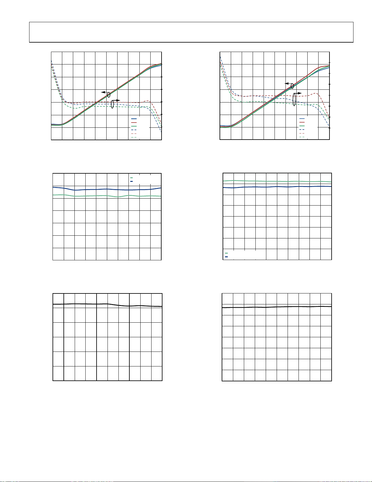
Figure 11. Gain Conformance over Temperature for VGA1
35
30
25
20
15
OIP3 (dBm re: 200Ω)
10
5
0
0 100 200 300 4 00 500 600 700 800 900 1000
GAIN1 (mV)
Figure 12. OIP3 vs. V
over Gain Code for VGA1
GAIN
GAIN CODE 11
GAIN CODE 00
30
3
2
1
0
ERROR (dB)
–1
–2
–3
09550-011
20
15
10
5
AGE GAIN ( dB)
VOL
0
–5
–10
0 100 200 300 400 500 600 700 800 900 1000
GAIN1 (mV)
–40°C
+25°C
+85°C
–40°C
+25°C
+85°C
3
2
1
0
ERROR (dB)
–1
–2
–3
–4
09550-014
Figure 14. Gain Conformance over Temperature for VGA2
28
23
18
13
8
OIP3 (dBV)
3
–2
–7
09550-114
40
35
30
25
20
15
OIP3 (d Bm re: 100Ω)
10
5
GAIN CODE 11
GAIN CODE 00
0
0 100 200 300 400 500 600 700 800 900 1000
GAIN2 (mV)
Figure 15. OIP3 vs. V
over Gain Code for VGA2
GAIN
30
25
20
15
10
5
0
–5
–10
OIP3 (dBV)
09550-017
23
40
30
25
20
re: 200Ω)
15
10
OIP3 (dB
5
0
4.54.64.74.84.95.05.15.25.35.45.5
VPOS (V)
Figure 13. OIP3 vs. Supply Voltage at V
= 0.5 V for VGA1
GAIN
18
13
8
OIP3 (dBV)
3
–2
–7
09550-015
35
30
25
20
15
OIP3 (dBm re: 100Ω)
10
5
0
4.5 4.6 4.7 4.8 4.9 5.0 5.1 5.2 5.3 5.4 5.5
VPOS (V)
Figure 16. OIP3 vs. Supply Voltage at V
= 0.5 V for VGA2
GAIN
25
20
15
10
5
0
–5
–10
OIP3 (dBV)
09550-018
Rev. A | Page 9 of 32
ADL5336
40
35
30
25
20
15
OIP3 (dBm re: 200Ω)
10
5
0
0 50 100 150 200 250 300 350 400 450 500
FREQUENC Y (MHz)
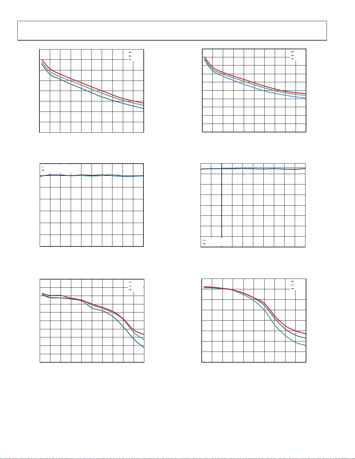
Figure 17. OIP3 vs. Frequency over Temperature for VGA1
14
GAIN CODE 11
GAIN CODE 00
12
10
8
6
OP1dB (dBm re: 200Ω)
4
2
0
0 0.1 0.2 0.3 0.4 0.5 0.6 0.7 0.8 0.9 1.0
GAIN1 (V)
Figure 18. OP1dB vs. V
over Gain Code for VGA1
GAIN
15
13
11
9
7
5
3
1
OP1dB (d Bm re: 200Ω)
–1
–3
–5
0 50 100 150 200 250 300 350 4 00 450 500
FREQUENC Y (MHz)
Figure 19. OP1dB vs. Frequency over Temperature for VGA1
–40°C
+25°C
+85°C
–40°C
+25°C
+85°C
33
28
23
18
13
8
3
–2
–7
7
5
3
1
–1
–3
–5
–7
8
6
4
2
0
–2
–4
–6
–8
–10
–12
50
45
40
35
30
25
OIP3 (dBV)
09550-013
20
OIP3 (d Bm re: 100Ω)
15
10
5
0
0 50 100 150 200 250 300 350 400 450 500
FREQUENC Y (MHz)
–40°C
+25°C
+85°C
40
35
30
25
20
15
10
5
0
–5
–10
OIP3 (dBV)
09550-016
Figure 20. OIP3 vs. Frequency over Temperature for VGA2
16
14
12
10
8
OP1dB (dBV)
09550-020
6
OP1dB (d Bm re: 100Ω)
4
2
GAIN CODE 11
GAIN CODE 00
0
0 0.10.20.30.40.50.60.70.80.91.0
GAIN2 (V)
Figure 21. OP1dB vs. V
over Gain Code for VGA2
GAIN
6
4
2
0
–2
–4
–6
–8
–10
OP1dB (d BV)
09550-022
16
14
12
10
8
OP1dB (dBV )
09550-019
6
OP1dB (dBm re: 100Ω)
4
2
0
0 50 100 150 200 250 300 350 400 450 500
FREQUENCY (MHz)
–40°C
+25°C
+85°C
6
4
2
0
–2
–4
–6
–8
–10
OP1dB (d BV)
09550-021
Figure 22. OP1dB vs. Frequency over Temperature for VGA2
Rev. A | Page 10 of 32
 Loading...