10 MHz to 3 GHz VGA with
www.BDTIC.com/ADI
FEATURES
Voltage-controlled amplifier/attenuator
Operating frequency 10 MHz to 3 GHz
Optimized for controlling output power
High linearity: OIP3 31 dBm @ 900 MHz
Output noise floor: −150 dBm/Hz @ 900 MHz
50 Ω input and output impedances
Single-ended or differential operation
Wide gain-control range: −34 dB to +22 dB @ 900 MHz
Linear-in-dB gain control function, 20 mV/dB
Single-supply 4.75 V to 5.25 V
APPLICATIONS
Transmit and receive power control at RF and IF
GENERAL DESCRIPTION
The ADL5330 is a high performance, voltage-controlled
variable gain amplifier/attenuator for use in applications with
frequencies up to 3 GHz. The balanced structure of the signal
path minimizes distortion while it also reduces the risk of
spurious feed-forward at low gains and high frequencies caused
by parasitic coupling. While operation between a balanced
source and load is recommended, a single-sided input is
internally converted to differential form.
The input impedance is 50 Ω from INHI to INLO. The outputs
a
re usually coupled into a 50 Ω grounded load via a 1:1 balun. A
single supply of 4.75 V to 5.25 V is required.
The 50 Ω input system converts the applied voltage to a pair of
ferential currents with high linearity and good common
dif
rejection even when driven by a single-sided source. The signal
currents are then applied to a proprietary voltage-controlled
attenuator providing precise definition of the overall gain under
the control of the linear-in-dB interface. The GAIN pin accepts
a voltage from 0 V at minimum gain to 1.4 V at full gain with a
20 mV/dB scaling factor.
60 dB Gain Control Range
ADL5330
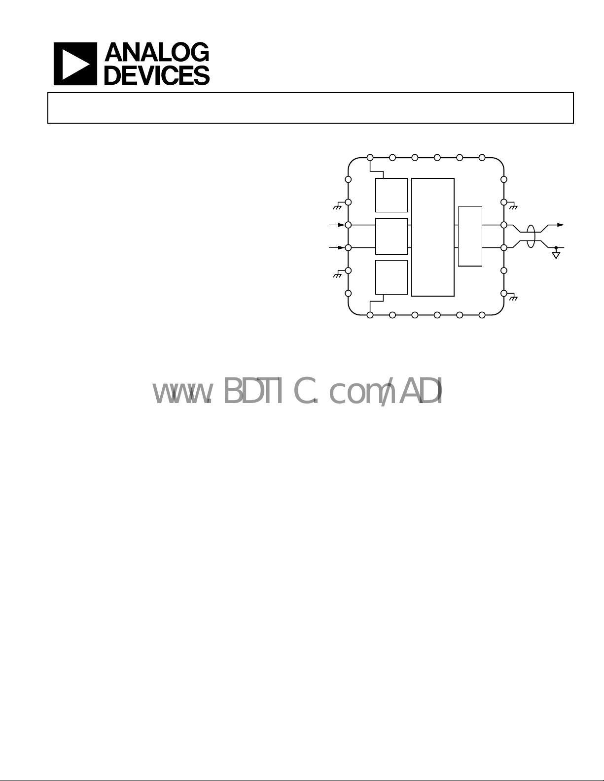
FUNCTIONAL BLOCK DIAGRAM
VPS2
VARIABLE
ATTENUATOR
CONTINUOUSLY
Figure 1.
VPS2VPS2
STAGE
COM2
O/P
(TZ)
COM2COM1OPBS
VPS2
COM2
OPHI
OPLO
COM2
VPS2
RFOUT
BALUN
GAIN
VPS1
COM1
INHI
RFIN
INLO
COM1
VPS1
VREF
ENBL VPS2
GAIN
CONTROL
INPUT
GM
STAGE
BIAS
AND
VREF
IPBS
The output of the high accuracy wideband attenuator is applied
to
a differential transimpedance output stage. The output stage
sets the 50 Ω differential output impedances and drives
Pin OPHI and Pin OPLO. The ADL5330 has a power-down
function. It can be powered down by a Logic LO input on the
ENBL pin. The current consumption in power-down mode is
250 μA.
The ADL5330 is fabricated on an ADI proprietary high
erformance, complementary bipolar IC process. The ADL5330
p
is available in a 24-lead (4 mm × 4 mm), Pb-free LFCSP_VQ
package and is specified for operation from ambient
temperatures of −40°C to +85°C. An evaluation board is also
available.
05134-001
Rev. A
Information furnished by Analog Devices is believed to be accurate and reliable.
However, no responsibility is assumed by Analog Devices for its use, nor for any
infringements of patents or other rights of third parties that may result from its use.
Specifications subject to change without notice. No license is granted by implication
or otherwise under any patent or patent rights of Analog Devices. Trademarks and
registered trademarks are the property of their respective owners.
One Technology Way, P.O. Box 9106, Norwood, MA 02062-9106, U.S.A.
Tel: 781.329.4700 www.analog.com
Fax: 781.461.3113 © 2005 Analog Devices, Inc. All rights reserved.

ADL5330
www.BDTIC.com/ADI
TABLE OF CONTENTS
Specifications..................................................................................... 3
Absolute Maximum Ratings............................................................ 5
ESD Caution.................................................................................. 5
Pin Configuration and Function Descriptions............................. 6
Typical Performance Characteristics............................................. 7
Theory of Operation ...................................................................... 12
Applications..................................................................................... 13
Basic Connections...................................................................... 13
RF Input/Output Interface ........................................................ 14
REVISION HISTORY
6/05—Rev. 0 to Rev. A
Changes to Figure 1.......................................................................... 1
Changes to Table 1............................................................................ 3
Changes to Table 2............................................................................ 5
Changes to Table 3............................................................................ 6
Changes to Figure 27...................................................................... 11
Changes to Figure 35...................................................................... 14
Changes to the Gain Control Input Section................................ 15
Changes to Figure 42...................................................................... 17
Gain Control Input .................................................................... 15
Automatic Gain Control............................................................ 15
Interfacing to an IQ Modulator................................................ 17
WCDMA Transmit Application ............................................... 18
CDMA2000 Transmit Application........................................... 19
Soldering Information ............................................................... 19
Evaluation Board ........................................................................ 20
Outline Dimensions ....................................................................... 24
Ordering Guide .......................................................................... 24
4/05—Revision 0: Initial Version
Rev. A | Page 2 of 24

ADL5330
www.BDTIC.com/ADI
SPECIFICATIONS
VS = 5 V; TA = 25°C; M/A-COM ETC1-1-13 1:1 balun at input and output for single-ended 50 Ω match.
Table 1.
Parameter Conditions Min Typ Max Unit
GENERAL
Usable Frequency Range 0.01 3 GHz
Nominal Input Impedance Via 1:1 single-sided-to-differential balun 50 Ω
Nominal Output Impedance Via 1:1 differential-to-single-sided balun 50 Ω
100 MHz
Gain Control Span ±3 dB gain law conformance 58 dB
Maximum Gain V
Minimum Gain V
Gain Flatness vs. Frequency
Gain Control Slope 20.7 mV/dB
Gain Control Intercept Gain = 0 dB, gain = slope (V
Input Compression Point V
Input Compression Point V
Output Third-Order Intercept (OIP3) V
Output Noise Floor
1
Noise Figure V
Input Return Loss
Output Return Loss
2
2
450 MHz
Gain Control Span ±3 dB gain law conformance 57 dB
Maximum Gain V
Minimum Gain V
Gain Flatness vs. Frequency
Gain Control Slope 20.4 mV/dB
Gain Control Intercept Gain = 0 dB, gain = slope (V
Input Compression Point V
Input Compression Point V
Output Third-Order Intercept (OIP3) V
Output Noise Floor
1
Noise Figure V
Input Return Loss
Output Return Loss
2
2
900 MHz
Gain Control Span ±3 dB gain law conformance 53 dB
Maximum Gain V
Minimum Gain V
Gain Flatness vs. Frequency
Gain Control Slope 19.7 mV/dB
Gain Control Intercept Gain = 0 dB, gain = slope (V
Input Compression Point V
Input Compression Point V
Output Third-Order Intercept (OIP3) V
Output Noise Floor
1
Noise Figure V
Input Return Loss
Output Return Loss
2
2
= 1.4 V 23 dB
GAIN
= 0.1 V −35 dB
GAIN
±30 MHz around center frequency,
= 1.0 V (differential output)
V
GAIN
− intercept) 0.88 V
GAIN
= 1.2 V 1.8 dBm
GAIN
= 1.4 V −0.3 dBm
GAIN
= 1.4 V 38 dBm
GAIN
20 MHz carrier offset, V
= 1.4 V 7.8 dB
GAIN
1 V < V
< 1.4 V −12.8 dB
GAIN
= 1.4 V −140 dBm/Hz
GAIN
0.09 dB
−15.5 dB
= 1.4 V 22 dB
GAIN
= 0.1 V −35 dB
GAIN
±30 MHz around center frequency,
V
= 1.0 V, (differential output)
GAIN
− intercept) 0.89 V
GAIN
= 1.2 V 3.3 dBm
GAIN
= 1.4 V 1.2 dBm
GAIN
= 1.4 V 36 dBm
GAIN
20 MHz carrier offset, V
= 1.4 V 8.0 dB
GAIN
1 V < V
< 1.4 V −19 dB
GAIN
= 1.4 V −146 dBm/Hz
GAIN
0.08 dB
−13.4 dB
= 1.4 V 21 dB
GAIN
= 0.2 V −32 dB
GAIN
±30 MHz around center frequency,
V
= 1.0 V (differential output)
GAIN
− intercept) 0.92 V
GAIN
= 1.2 V 2.7 dBm
GAIN
= 1.4 V 1.3 dBm
GAIN
= 1.4 V 31.5 dBm
GAIN
20 MHz carrier offset, V
= 1.4 V 9.0 dB
GAIN
1 V < V
< 1.4 V −18 dB
GAIN
= 1.4 V −144 dBm/Hz
GAIN
0.14 dB
−18 dB
Rev. A | Page 3 of 24

ADL5330
www.BDTIC.com/ADI
Parameter Conditions Min Typ Max Unit
2200 MHz
Gain Control Span ±3 dB gain law conformance 46 dB
Maximum Gain V
Minimum Gain V
Gain Flatness vs. Frequency
Gain Control Slope 16.7 mV/dB
Gain Control Intercept Gain = 0 dB, gain = slope (V
Input Compression Point V
Input Compression Point V
Output Third-Order Intercept (OIP3) V
Output Noise Floor
1
Noise Figure V
Input Return Loss
Output Return Loss
2
2
2700 MHz
Gain Control Span ±3 dB gain law conformance 42 dB
Maximum Gain V
Minimum Gain V
Gain Flatness vs. Frequency
Gain Control Slope 16 mV/dB
Gain Control Intercept Gain = 0 dB, gain = slope (V
Input Compression Point V
Input Compression Point V
Output Third-Order Intercept (OIP3) V
Output Noise Floor
1
Noise Figure V
Input Return Loss
Output Return Loss
2
2
GAIN CONTROL INPUT GAIN pin
Gain Control Voltage Range
3
Incremental Input Resistance GAIN pin to COM1 pin 1 MΩ
Response Time Full scale: to within 1 dB of final gain 380 ns
3 dB gain step, P
POWER SUPPLIES Pin VPS1, Pin VPS2, Pin COM1, Pin COM2, Pin ENBL
Voltage 4.75 5 5.25 V
Current, Nominal Active VGN = 0 V 100 mA
V
Current, Disabled ENBL = LO 250 μA
1
Noise floor varies slightly with output power level. See Figure 9 through Figure 13.
2
See Figure 27 and Figure 29 for differential input and output impedances.
3
Minimum gain voltage varies with frequency. See Figure 3 through Figure 7.
= 1.4 V 16 dB
GAIN
= 0.6 V −30 dB
GAIN
±30 MHz around center frequency,
= 1.0 V (differential output)
V
GAIN
− intercept) 1.06 V
GAIN
= 1.2 V 0.9 dBm
GAIN
= 1.4 V −2.0 dBm
GAIN
= 1.4 V 21.2 dBm
GAIN
20 MHz carrier offset, V
= 1.4 V 12.5 dB
GAIN
1 V < V
< 1.4 V −11.7 dB
GAIN
= 1.4 V −147 dBm/Hz
GAIN
0.23 dB
−9.5 dB
= 1.4 V 10 dB
GAIN
= 0.7 V −32 dB
GAIN
±30 MHz around center frequency,
= 1.0 V (differential output)
V
GAIN
− intercept) 1.15 V
GAIN
= 1.2 V 1.2 dBm
GAIN
= 1.4 V −0.9 dBm
GAIN
= 1.4 V 17 dBm
GAIN
20 MHz carrier offset, V
= 1.4 V 14.7 dB
GAIN
1 V < V
< 1.4 V −9.7 dB
GAIN
= 1.4 V −152 dBm/Hz
GAIN
0.3 dB
−5 dB
0 1.4 V
to within 1 dB of final gain 20 ns
OUT
= 1.4 V 215 mA
GN
Rev. A | Page 4 of 24

ADL5330
www.BDTIC.com/ADI
ABSOLUTE MAXIMUM RATINGS
Table 2.
Parameter Rating
Supply Voltage VPS1, VPS2 5.5 V
RF Input Power at Maximum Gain 5 dBm at 50 Ω
OPHI, OPLO 5.5 V
ENBL VPS1, VPS2
GAIN 2.5 V
Internal Power Dissipation 1.1 W
θJA (with Pad Soldered to Board) 60°C/W
Maximum Junction Temperature 150°C
Operating Temperature Range −40°C to +85°C
Storage Temperature Range −65°C to +150°C
Lead Temperature Range (Soldering 60 sec) 300°C
ESD CAUTION
ESD (electrostatic discharge) sensitive device. Electrostatic charges as high as 4000 V readily accumulate on
the human body and test equipment and can discharge without detection. Although this product features
proprietary ESD protection circuitry, permanent damage may occur on devices subjected to high energy
electrostatic discharges. Therefore, proper ESD precautions are recommended to avoid performance
degradation or loss of functionality.
Stresses above those listed under Absolute Maximum Ratings
may cause permanent damage to the device. This is a stress
rating only; functional operation of the device at these or any
other conditions above those indicated in the operational
section of this specification is not implied. Exposure to absolute
maximum rating conditions for extended periods may affect
device reliability.
Rev. A | Page 5 of 24

ADL5330
C
C
www.BDTIC.com/ADI
PIN CONFIGURATION AND FUNCTION DESCRIPTIONS
GAIN
ENBL
VPS2
VPS2
VPS2
2322212019
PIN 1
INDICATOR
11
10
IPBS
OPBS
GNLO
COM1
VPS2
12
COM2
18
17
16
15
14
13
VPS2
COM2
OPHI
OPLO
COM2
VPS2
05134-002
24
VPS1
1
OM1
2
INHI
3
ADL5330
4
INLO
OM1
VPS1
5
6
TOP VIEW
(Not to Scale)
789
VREF
Figure 2. Pin Configuration
Table 3. Pin Function Descriptions
Pin No. Mnemonic Descriptions
1, 6, 13, 18 to 22 VPS1, VPS2 Positive Supply. Nominally equal to 5 V.
2, 5, 10 COM1 Common for Input Stage.
3, 4 INHI, INLO Differential Inputs, AC-Coupled.
7 VREF Voltage Reference. Output at 1.5 V; normally ac-coupled to ground.
8 IPBS Input Bias. Normally ac-coupled to ground.
9 OPBS Output Bias. AC-Coupled to ground.
11 GNLO Gain Control Common. Connect to ground.
12, 14, 17 COM2 Common for Output Stage.
15 OPLO Low Side of Differential Output. Bias to VP with RF chokes.
16 OPHI High Side of Differential Output. Bias to VP with RF chokes.
23 ENBL Device Enable. Apply logic high for normal operation.
24 GAIN Gain Control Voltage Input. Nominal range 0 V to 1.4 V.
Rev. A | Page 6 of 24

ADL5330
www.BDTIC.com/ADI
TYPICAL PERFORMANCE CHARACTERISTICS
GAIN (dB)
GAIN (dB)
GAIN (dB)
30
20
10
0
–10
–20
+85°C GAIN
–30
–40
–50
+25°C GAIN
–40°C GAIN
V
GAIN
(V)
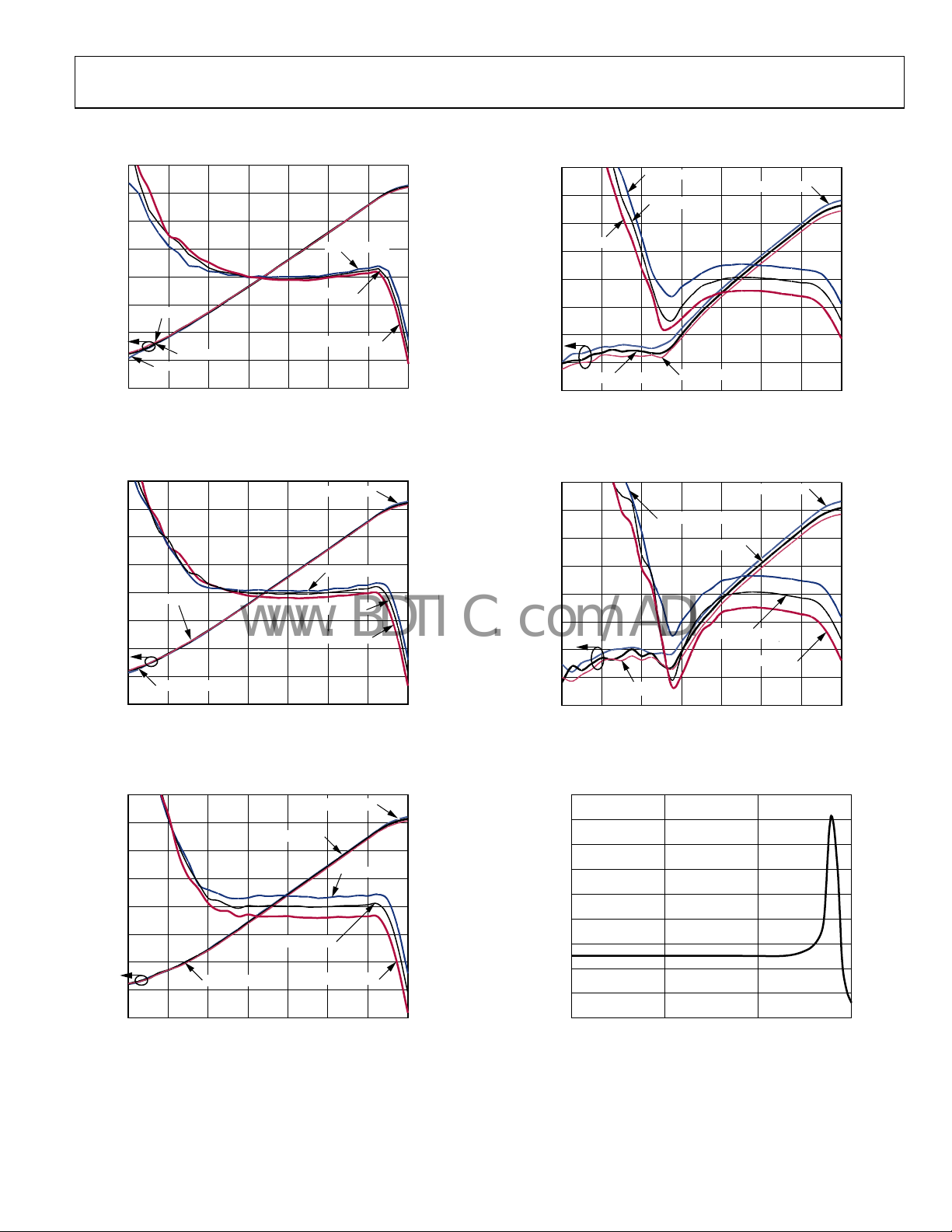
Figure 3. Gain and Gain Law Conformance vs. V
over Temperature at 100 MHz
30
20
10
0
–10
+85°C GAIN
–20
–30
–40
–50
+25°C GAIN
V
GAIN
(V)
Figure 4. Gain and Gain Law Conformance vs. V
over Temperature at 450 MHz
30
–10
–20
–30
–40
–50
20
10
0
+85°C GAIN
+25°C GAIN
+25°C ERROR
V
(V)
GAIN
Figure 5. Gain and Gain Law Conformance vs. V
over Temperature at 900 MHz
–40°C ERROR
+25°C ERROR
+85°C ERROR
–40°C GAIN
–40°C ERROR
+25°C ERROR
+85°C ERROR
–40°C GAIN
–40°C ERROR
+85°C ERROR
GAIN
GAIN
GAIN
4
3
2
1
0
–1
–2
GAIN LAW CONFORMANCE (dB)
–3
–4
1.40 0.2 0.4 0.6 0.8 1.0 1.2
05134-003
–10
GAIN (dB)
–20
–30
–40
–50
30
20
10
+85°C ERROR
0
+25°C GAIN
–40°C ERROR
+25°C ERROR
+85°C GAIN
V
GAIN
(V)
Figure 6. Gain and Gain Law Conformance vs. V
–40°C GAIN
GAIN
12
9
6
3
0
–3
–6
GAIN LAW CONFORMANCE (dB)
–9
–12
1.40 0.2 0.4 0.6 0.8 1.0 1.2
over Temperature at 2200 MHz
4
3
2
1
0
–1
–2
GAIN LAW CONFORMANCE (dB)
–3
–4
1.40 0.2 0.4 0.6 0.8 1.0 1.2
05134-004
20
10
0
–10
–20
GAIN (dB)
–30
–40
–50
–60
+85°C GAIN
–40°C ERROR
+25°C GAIN
V
(V)
GAIN
–40°C GAIN
+25°C ERROR
+85°C ERROR
Figure 7. Gain and Gain Law Conformance vs. V
GAIN
12
9
6
3
0
–3
–6
GAIN LAW CONFORMANCE (dB)
–9
–12
1.40 0.2 0.4 0.6 0.8 1.0 1.2
over Temperature at 2700 MHz
4
3
2
1
0
–1
–2
GAIN LAW CONFORMANCE (dB)
–3
–4
1.40 0.2 0.4 0.6 0.8 1.0 1.2
05134-005
180
160
140
120
100
80
60
40
GAIN CONTROL SLOPE (dB/V)
20
0
FREQUENCY (kHz)
Figure 8. Frequency Response of Gain Control Input,
Carr
ier Frequency = 900 MHz
V
GAIN
= 1.0V
10,00010 100 1,000
05134-008
05134-006
05134-007
Rev. A | Page 7 of 24

ADL5330
www.BDTIC.com/ADI
40
30
OIP3
–115
–120
30
20
OIP3
–115
–120
20
10
0
–10
POWER (dBm)
–20
–30
–40
INPUT P1dB
V
GAIN
OUTPUT P1dB
(V)
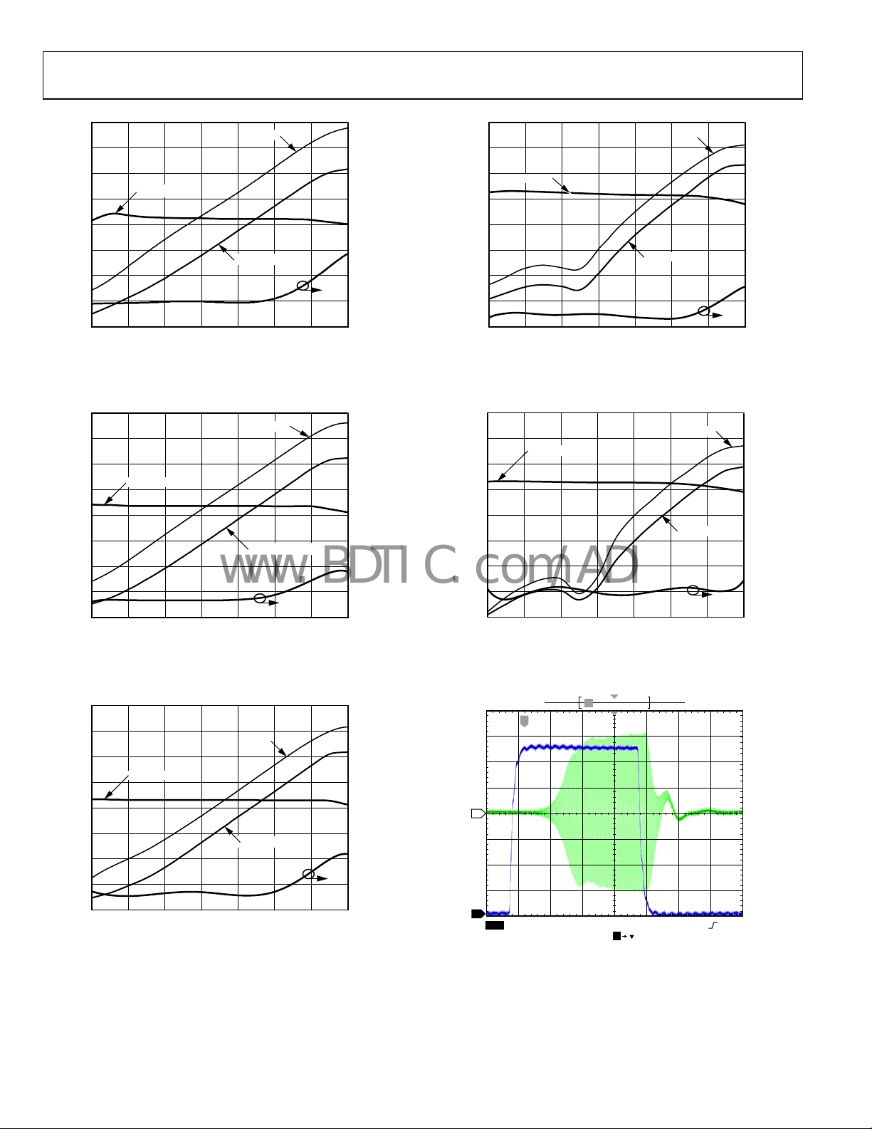
Figure 9. Input Compression Point, Output Compression Point,
OIP3,
and Noise Floor vs. V
40
30
20
10
0
–10
POWER (dBm)
–20
INPUT P1dB
at 100 MHz
GAIN
OIP3
OUTPUT P1dB
–125
–130
–135
–140
–145
–150
–155
1.40 0.2 0.4 0.6 0.8 1.0 1.2
–115
–120
–125
–130
–135
–140
–145
NOISE FLOOR (dBm/Hz)
05134-009
NOISE FLOOR (dBm/Hz)
10
INPUT P1dB
0
–10
–20
POWER (dBm)
–30
–40
–50
V
GAIN
OUTPUT P1dB
(V)
Figure 12. Input Compression Point, Output Compression Point,
OIP3,
and Noise Floor vs. V
30
20
10
0
–10
–20
POWER (dBm)
–30
INPUT P1dB
at 2200 MHz
GAIN
OIP3
OUTPUT P1dB
–125
–130
–135
–140
–145
NOISE FLOOR (dBm/Hz)
–150
–155
1.40 0.2 0.4 0.6 0.8 1.0 1.2
–120
–125
–130
–135
–140
–145
–150
05134-012
NOISE FLOOR (dBm/Hz)
–30
–40
(V)
V
GAIN
Figure 10. Input Compression Point, Output Compression Point,
GAIN
OIP3
OUTPUT P1dB
(V)
at 450 MHz
40
30
20
10
0
–10
POWER (dBm)
–20
–30
–40
OIP3,
and Noise Floor vs. V
INPUT P1dB
V
GAIN
Figure 11. Input Compression Point, Output Compression Point,
OIP3,
and Noise Floor vs. V
at 900 MHz
GAIN
–150
–155
1.40 0.40.2 0.80.6 1.0 1.2
05134-010
–40
–50
V
(V)
GAIN
–155
–160
1.40 0.2 0.4 0.6 0.8 1.0 1.2
05134-013
Figure 13. Input Compression Point, Output Compression Point,
OIP3,
and Noise Floor vs. V
–115
–120
–125
–130
–135
–140
–145
NOISE FLOOR (dBm/Hz)
–150
–155
1.40 0.40.2 0.6 0.8 1.0 1.2
05134-011
2
1
T
CH1 200mV CH2 100mV Ω M100ns A CH4 2.70V
T
T 382.000ns
at 2700 MHz
GAIN
05134-014
Figure 14. Step Response of Gain Control Input
Rev. A | Page 8 of 24
 Loading...