

400 MHz to 4000 MHz
–
Data Sheet
FEATURES
Operation from 400 MHz to 4000 MHz
Gain of 14.6 dB at 2140 MHz
OIP3 of 43.1 dBm at 2140 MHz
P1dB of 29.1 dBm at 2140 MHz
Noise figure of 3.8 dB
Dynamically adjustable bias
Adjustable power supply bias: 3.3 V to 5 V
Low power supply current: 62 mA to 133 mA
No bias resistor needed
Operating temperature range of −40°C to +105°C
SOT-89 package, MSL-1 rated
ESD rating of ±3 kV (Class 2)
APPLICATIONS
Wireless infrastructure
Automated test equipment
ISM/AMR applications
GENERAL DESCRIPTION
The ADL5324 incorporates a dynamically adjustable biasing
circuit that allows for the customization of OIP3 and P1dB
performance from 3.3 V to 5 V, without the need for an external
bias resistor. This feature gives the designer the ability to tailor
driver amplifier performance to the specific needs of the design.
This feature also creates the opportunity for dynamic biasing of
the driver amplifier where a variable supply is used to allow for
full 5 V biasing under large signal conditions, and then reduced
supply voltage when signal levels are smaller and lower power
consumption is desirable. This scalability reduces the need to
evaluate and inventory multiple driver amplifiers for different
output power requirements, from 25 dBm to 29 dBm output
power levels.
The ADL5324 is also rated to operate across the wide temperature range of −40°C to +105°C for reliable performance
in designs that experience higher temperatures, such as power
amplifiers. The ½ W driver amplifier also covers the wide
frequency range of 400 MHz to 4000 MHz, and only requires
a few external components to be tuned to a specific band within
that wide range. This high performance broadband RF driver
amplifier is well suited for a variety of wired and wireless
applications, including cellular infrastructure, ISM band power
amplifiers, defense equipment, and instrumentation equipment.
A fully populated evaluation board is available.
½ Watt RF Driver Amplifier
ADL5324
FUNCTIONAL BLOCK DIAGRAM
GND
(2)
ADL5324
BIAS
1 2
RFIN
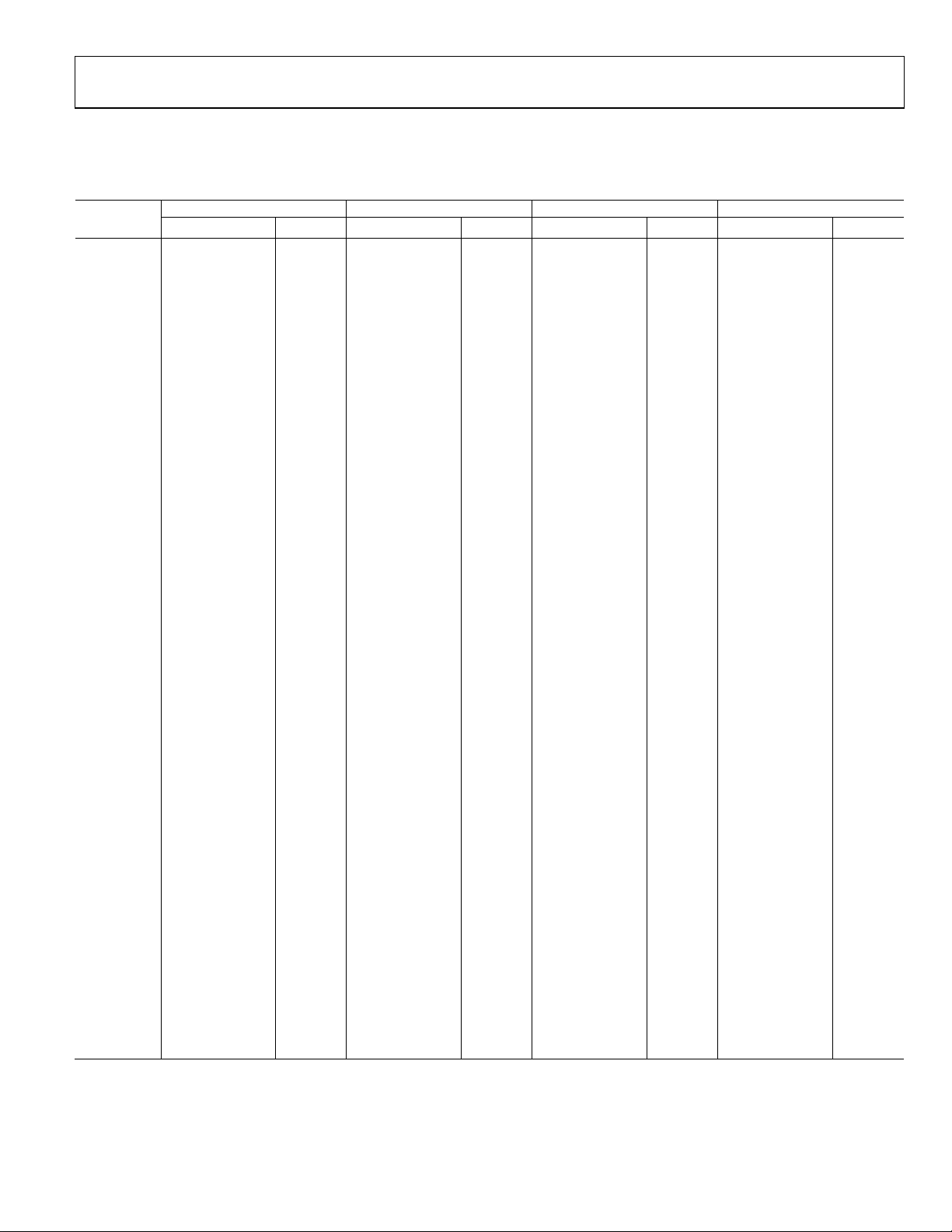
The ADL5324 also delivers excellent ACPR vs. output power
and bias voltage. The driver can deliver greater than 17 dBm
of output power at 2140 MHz, while achieving an ACPR of
−55 dBc at 5 V. If the bias is reduced to 3.3 V, the −55 dBc
ACPR output power only minimally reduces to 15 dBm.
30
–35
–40
–45
–50
–55
–60
–65
–70
–75
ACPR @ 5MHz CARRIER O FFSET (dBc)
–80
–85
–20 –15 –10 –5 0 5 10 15 20 25
Figure 2. ACPR vs. Output Power, Single Carrier W-CDMA,
SOURCE
VCC=3.3V
VCC=5V
TM1-64 at 2140 MHz
GND
RFOUT
Figure 1.
P
(dBm)
OUT
3
10562-001
10562–055
Rev. 0
Information furnished by Analog Devices is believed to be accurate and reliable. However, no
responsibility is assumed by Analog Devices for its use, nor for any infringements of patents or other
rights of third parties that may result from its use. Specifications subject to change without notice. No
license is granted by implication or otherwise under any patent or patent rights of Analog Devices.
Trademarks and registered trademarks are the property of their respective owners.
One Technology Way, P.O. Box 9106, Norwood, MA 02062−9106, U.S.A.
Tel: 781.329.4700 www.analog.com
Fax: 781.461.3113 ©2012 Analog Devices, Inc. All rights reserved.

ADL5324 Data Sheet
TABLE OF CONTENTS
Features .............................................................................................. 1
Applications ....................................................................................... 1
Functional Block Diagram .............................................................. 1
General Description ......................................................................... 1
Revision History ............................................................................... 2
Specifications ..................................................................................... 3
Typical Scattering Parameters ..................................................... 5
Absolute Maximum Ratings ............................................................ 6
ESD Caution .................................................................................. 6
Pin Configuration and Function Descriptions ............................. 7
Typical Performance Characteristics ............................................. 8
REVISION HISTORY
3/12—Revision 0: Initial Version
High Temperature Operation ................................................... 12
Applications Information .............................................................. 13
Basic Layout Connections ......................................................... 13
Soldering Information and Recommended PCB Land
Pattern .......................................................................................... 13
Matching Procedure ................................................................... 15
W-CDMA ACPR Performance ................................................ 16
Evaluation Board ............................................................................ 17
Outline Dimensions ....................................................................... 20
Ordering Guide .......................................................................... 20
Rev. 0 | Page 2 of 20

Data Sheet ADL5324
OUT
Output 1 dB Compression Point
24.2
28.0 dBm
OUT
OUT
FREQUENCY = 1935 MHz
OUT
Output Third-Order Intercept
∆f = 1 MHz, P
OUT
= 10 dBm per tone
34.4
43.1 dBm
SPECIFICATIONS
VSUP = 5 V and TA = 25°C, unless otherwise noted.
Table 1.
3.3 V 5 V
Parameter Test Conditions/Comments Min Typ Max Min Typ Max Unit
FREQUENCY = 457 MHz
Gain 17.2 18.4 dB
vs. Frequency ±37 MHz +0.0/−0.4 +0.0/−0.2 dB
vs. Temperature −40°C ≤ TA ≤ +85°C ±0.6 ±0.6 dB
vs. Supply 3.15 V to 3.45 V, 4.75 V to 5.25 V ±0.3 ±0.07 dB
Output 1 dB Compression Point 24.2 28.0 dBm
Output Third-Order Intercept ∆f = 1 MHz, P
Noise Figure 5.6 6.8 dB
FREQUENCY = 748 MHz
Gain 16.5 17.5 dB
vs. Frequency ±20 MHz +0.0/−0.2 +0.0/−0.2 dB
vs. Temperature −40°C ≤ TA ≤ +85°C ±0.4 ±0.4 dB
vs. Supply 3.15 V to 3.45 V, 4.75 V to 5.25 V ±0.2 ±0.06 dB
= 10 dBm per tone 30.1 40.1 dBm
Output Third-Order Intercept ∆f = 1 MHz, P
= 10 dBm per tone 36.0 45.8 dBm
Noise Figure 4.0 5.2 dB
FREQUENCY = 915 MHz
Gain1 15.8 16.0 16.8 17.6 dB
vs. Frequency ±46 MHz ±0.1 +0.1/−0.3 dB
vs. Temperature −40°C ≤ TA ≤ +85°C ±0.4 ±0.4 dB
vs. Supply 3.15 V to 3.45 V, 4.75 V to 5.25 V ±0.2 ±0.06 dB
Output 1 dB Compression Point 24.2 27.7 dBm
Output Third-Order Intercept ∆f = 1 MHz, P
= 10 dBm per tone 39.3 45.6 dBm
Noise Figure 4.1 5.1 dB
Gain 13.9 15.0 dB
vs. Frequency ±55 MHz +0.0/−0.1 +0.0/−0.1 dB
vs. Temperature −40°C ≤ TA ≤ +85°C ±0.5 ±0.5 dB
vs. Supply 3.15 V to 3.45 V, 4.75 V to 5.25 V ±0.2 ±0.07 dB
Output 1 dB Compression Point 23.2 27.2 dBm
Output Third-Order Intercept ∆f = 1 MHz, P
= 10 dBm per tone 34.6 45.5 dBm
Noise Figure 3.1 3.6 dB
FREQUENCY = 2140 MHz
Gain1 13.6 13.5 14.6 15.7 dB
vs. Frequency ±30 MHz +0.1/−0.0 ±0.1 dB
vs. Temperature −40°C ≤ TA ≤ +85°C ±0.6 ±0.6 dB
vs. Supply 3.15 V to 3.45 V, 4.75 V to 5.25 V ±0.2 ±0.06 dB
Output 1 dB Compression Point 25.3 29.1 dBm
Noise Figure 3.2 3.8 dB
Rev. 0 | Page 3 of 20

ADL5324 Data Sheet
OUT
vs. Temperature
−40°C ≤ TA ≤ +85°C
±1.0
±1.0 dB
OUT
3.3 V 5 V
Parameter Test Conditions/Comments Min Typ Max Min Typ Max Unit
FREQUENCY = 2630 MHz
Gain1 12.1 11.8 13.3 14.6 dB
vs. Frequency ±60 MHz ±0.1 +0.0/−0.2 dB
vs. Temperature −40°C ≤ TA ≤ +85°C ±0.7 ±0.7 dB
vs. Supply 3.15 V to 3.45 V, 4.75 V to 5.25 V ±0.2 ±0.07 dB
Output 1 dB Compression Point 23.6 27.8 dBm
Output Third-Order Intercept ∆f = 1 MHz, P
Noise Figure 3.6 4.3 dB
FREQUENCY = 3600 MHz
Gain 11.0 12.0 dB
vs. Frequency ±100 MHz +0.0/−0.7 +0.0/−0.8 dB
vs. Supply 3.15 V to 3.45 V, 4.75 V to 5.25 V ±0.2 ±0.05 dB
Output 1 dB Compression Point 25.0 28.5 dBm
Output Third-Order Intercept ∆f = 1 MHz, P
Noise Figure 3.8 4.4 dB
POWER INTERFACE Pin RFOUT
Supply Voltage 3.15 3.3 3.45 4.75 5 5.25 V
Supply Current 62 140 mA
vs. Temperature −40°C ≤ TA ≤ +85°C +4/−6 +5/−7 mA
Power Dissipation VSUP = 5 V 205 700 mW
1
Guaranteed maximum and minimum specified limits on this parameter are based on six sigma calculations.
= 10 dBm per tone 32.4 42.0 dBm
= 10 dBm per tone 29.3 36.6 dBm
Rev. 0 | Page 4 of 20
Data Sheet ADL5324
Freq (MHz)
S11
S21
S12
S22
Magnitude (dB)
Angle (°)
Magnitude (dB)
Angle (°)
Magnitude (dB)
Angle (°)
Magnitude (dB)
Angle (°)
TYPICAL SCATTERING PARAMETERS
VSUP = 5 V and TA = 25°C; the effects of the test fixture have been de-embedded up to the pins of the device.
Table 2.
400 −0.73518 −178.582 13.3917 135.7023 −34.6804 12.40754 −3.04567 175.7277
500 −0.6682 178.6472 12.83594 125.9539 −34.2707 8.733014 −3.13245 175.9202
600 −0.69026 176.9348 12.14674 117.8626 −34.1019 6.416618 −3.13132 176.4634
700 −0.73622 175.8152 11.44082 111.0321 −34.0009 5.053048 −3.11375 177.3131
800 −0.78026 175.0847 10.7709 105.1552 −33.9042 3.90523 −3.08891 178.3368
900 −0.8238 174.5898 10.17296 99.91559 −33.7964 3.162531 −3.05337 179.4021
1000 −0.8703 174.2026 9.636511 95.21821 −33.6656 2.580227 −3.01719 −179.377
1100 −0.9211 173.9872 9.182607 91.01039 −33.5057 2.111382 −2.98741 −177.773
1200 −0.97114 173.3143 8.797653 86.68882 −33.3176 1.186726 −2.94972 −176.469
1300 −1.05332 172.9788 8.493785 82.89921 −33.0916 0.689198 −2.9749 −174.745
1400 −1.13807 172.418 8.268673 79.01047 −32.8261 −0.26086 −2.99624 −173.189
1500 −1.23342 171.5538 8.117951 74.96804 −32.5253 −1.43036 −3.02533 −171.783
1600 −1.34406 170.302 8.030017 70.69309 −32.1979 −3.08241 −3.04592 −170.675
1700 −1.47125 168.6736 7.998348 66.16438 −31.8306 −5.10232 −3.05748 −169.736
1800 −1.61396 166.5204 8.012977 61.23666 −31.4647 −7.75224 −3.08106 −169.23
1900 −1.78541 163.8113 8.0503 55.89288 −31.0967 −10.9203 −3.12034 −169.149
2000 −1.98158 160.6247 8.103461 50.12853 −30.7409 −14.671 −3.15588 −169.657
2100 −2.19535 157.0149 8.162658 43.95115 −30.4109 −19.0255 −3.18172 −170.862
2200 −2.43367 153.0489 8.207579 37.39437 −30.1134 −23.849 −3.19212 −172.621
2300 −2.68863 148.8413 8.231765 30.52801 −29.872 −29.1849 −3.17831 −174.879
2400 −2.95983 144.5491 8.231791 23.39294 −29.6822 −35.0026 −3.13204 −177.553
2500 −3.25472 140.354 8.199665 16.05117 −29.5353 −41.1796 −3.05541 179.4875
2600 −3.56594 136.4445 8.141897 8.510386 −29.4496 −47.7908 −2.94631 176.2481
2700 −3.90734 133.0736 8.052657 0.787456 −29.4307 −54.7743 −2.79325 172.8794
2800 −4.28173 130.4779 7.925075 −7.06584 −29.451 −62.1914 −2.57604 169.6831
2900 −4.69306 128.952 7.778394 −15.0835 −29.5362 −69.9289 −2.31023 166.7304
3000 −5.13012 128.7774 7.590076 −23.2924 −29.673 −78.1809 −2.00734 164.1571
3100 −5.54712 130.3019 7.355608 −31.6367 −29.8658 −86.8436 −1.69231 162.0214
3200 −5.86482 133.6487 7.062082 −40.2413 −30.1507 −96.2073 −1.37649 160.0906
3300 −5.98131 138.5443 6.680613 −48.9518 −30.5191 −106.08 −1.0663 158.4485
3400 −5.80159 144.0974 6.20792 −57.556 −30.9857 −116.217 −0.80053 157.172
3500 −5.34159 149.2672 5.63213 −65.9828 −31.5373 −126.686 −0.58238 156.1642
3600 −4.7127 153.2749 4.988874 −73.9355 −32.1461 −137.413 −0.41604 155.491
3700 −4.03208 155.8906 4.279792 −81.4065 −32.7942 −148.125 −0.30331 155.1641
3800 −3.37391 157.3335 3.543499 −88.1911 −33.4212 −158.775 −0.23714 155.0734
3900 −2.79798 157.8681 2.803935 −94.5028 −33.9833 −169.303 −0.20674 155.156
4000 −2.30194 157.7622 2.085365 −100.344 −34.3781 −179.983 −0.20598 155.3378
Rev. 0 | Page 5 of 20
ADL5324 Data Sheet
JA
JC
ABSOLUTE MAXIMUM RATINGS
Table 3.
Parameter Rating
Supply Voltage, VSUP 6.5 V
Input Power (50 Ω Impedance) 20 dBm
Internal Power Dissipation (Paddle Soldered) 1.9 W
Maximum Junction Temperature 150°C
Operating Temperature Range −40°C to +105°C
Storage Temperature Range −65°C to +150°C
Stresses above those listed under Absolute Maximum Ratings
may cause permanent damage to the device. This is a stress
rating only; functional operation of the device at these or any
other conditions above those indicated in the operational
section of this specification is not implied. Exposure to absolute
maximum rating conditions for extended periods may affect
device reliability.
THERMAL RESISTANCE
Tabl e 4 lists the junction-to-air thermal resistance (θJA) and the
junction-to-paddle thermal resistance (θ
) for the ADL5324.
JC
Table 4. Thermal Resistance
Package Type θ
1
θ
2
Unit
3-Lead SOT-89 37 9 °C/W
1
Measured on Analog Devices evaluation board. For more information about
board layout, see the Soldering Information and Recommended PCB Land
Pattern section.
2
Based on simulation with JEDEC standard JESD51.
ESD CAUTION
Rev. 0 | Page 6 of 20

Data Sheet ADL5324
RFIN
GND
RFOUT
1
2
3
GND
ADL5324
TOP VIEW
(Not to Scale)
(2)
10562-002
3
RFOUT
RF Output and Supply Voltage. DC bias is provided to this pin through an inductor that is connected
PIN CONFIGURATION AND FUNCTION DESCRIPTIONS
Figure 3. Pin Configuration
Table 5. Pin Function Descriptions
Pin No. Mnemonic Description
1 RFIN RF Input. This pin requires a dc blocking capacitor.
2 GND Ground. Connect this pin to a low impedance ground plane.
Note that the paddle, which is exposed, encompasses Pin 2 and the tab at the top side of the package.
It should be soldered to a low impedance ground plane for electrical grounding and thermal transfer.
to the external power supply. The RF path requires a dc blocking capacitor.
Rev. 0 | Page 7 of 20

ADL5324 Data Sheet
50
0
869 884 900 915 930 946 961
NOISE FIGURE, GAIN, P1DB, OIP3 (dB, dBm)
FREQUENCY (MHz)
5
10
15
20
25
30
35
40
45
OIP3 (d Bm)
P1dB (dBm)
GAIN (dB)
NF (dB)
10562-015
17.5
15.5
16.0
16.5
17.0
869 884 900 915 930 946 961
GAIN (dB)
FREQUENCY (MHz)
–40°C
+25°C
+85°C
10562-016
0
–10
–15
–5
–40
869 961
S-PARAMETERS (dB)
FREQUENCY (MHz)
–30
–35
–25
–20
884 900 915 930 946
S11
S12
S22
10562-017
–40°C
–40°C
35
25
869 884 900 915 930 946 961
P1dB (dBm)
OIP3 (d Bm)
FREQUENCY (MHz)
+25°C
+85°C
+85°C
30
32
34
36
38
40
42
44
46
48
50
26
27
28
29
30
31
32
33
34
+25°C
10562-018
55
35
–5 0 5 10 15 20
OIP3 (d Bm)
P
OUT
PER TONE ( dBm)
37
39
41
43
45
47
49
51
53
869MHz
915MHz
961MHz
10562-019
7
3
869 961
NOISE FIGURE (dB)
FREQUENCY (MHz)
5
4
6
884 900 915 930 946
+85°C
+25°C
–40°C
10562-020
TYPICAL PERFORMANCE CHARACTERISTICS
Figure 4. Gain, P1dB, OIP3, and Noise Figure vs. Frequency,
869 MHz to 961 MHz
Figure 5. Gain vs. Frequency and Temperature, 869 MHz to 961 MHz
Figure 7. OIP3 and P1dB vs. Frequency and Temperature,
869 MHz to 961 MHz
Figure 8. OIP3 vs. P
and Frequency, 869 MHz to 961 MHz
OUT
Figure 6. Input Return Loss (S11), Output Return Loss (S22), and Reverse
Isolation (S12) vs. Frequency, 869 MHz to 961 MHz
Rev. 0 | Page 8 of 20
Figure 9. Noise Figure vs. Frequency and Temperature,
869 MHz to 961 MHz

Data Sheet ADL5324
50
0
2110 2120 2130 2140 2150 2160 2170
NOISE FIGURE, GAIN, P1dB, OIP3 (dB, dBm)
FREQUENCY (MHz)
5
10
15
20
25
30
35
40
45
OIP3 (d Bm)
P1dB (dBm)
GAIN (dB)
NF (dB)
10562-027
16.0
15.5
15.0
14.5
14.0
13.5
13.0
2110 2120 2130 2140 2150 2160 2170
GAIN (dB)
FREQUENCY (MHz)
10562-028
–40°C
+25°C
+85°C
0
–10
–15
–5
–40
2110 2170
S-PARAMETERS (dB)
FREQUENCY (MHz)
–30
–35
–25
–20
2120 2130 2140 2150 2160
S12
10562-029
S11
S22
–40°C
–40°C
35
25
2110 2120 2130 2140 2150 2160 2170
P1dB (dBm)
OIP3 (d Bm)
FREQUENCY (MHz)
+85°C
+85°C
28
30
32
34
36
38
40
42
44
46
48
26
27
28
29
30
31
32
33
34
10562-030
+25°C
+25°C
10562-031
2110MHz
2140MHz
2170MHz
50
48
30
42
40
38
36
34
32
44
46
–5 0 5 10 15 20
OIP3 (d Bm)
P
OUT
PER TONE ( dBm)
10562-032
6
5
2
2110 2170
NOISE FIGURE (dB)
FREQUENCY (MHz)
3
4
2120 2130 2140 2150 2160
–40°C
+25°C
+85°C
Figure 10. Gain, P1dB, OIP3, and Noise Figure vs. Frequency,
2110 MHz to 2170 MHz
Figure 11. Gain vs. Frequency and Temperature, 2110 MHz to 2170 MHz
Figure 13. OIP3 and P1dB vs. Frequency and Temperature,
2110 MHz to 2170 MHz
Figure 14. OIP3 vs. P
and Frequency, 2110 MHz to 2170 MHz
OUT
Figure 12. Input Return Loss (S11), Output Return Loss (S22), and Reverse
Isolation (S12) vs. Frequency, 2110 MHz to 2170 MHz
Rev. 0 | Page 9 of 20
Figure 15. Noise Figure vs. Frequency and Temperature,
2110 MHz to 2170 MHz

ADL5324 Data Sheet
10562-033
50
0
2570 2690
NOISE FIGURE, GAIN, P1dB, OIP3 (dB, dBm)
FREQUENCY (MHz)
5
10
15
20
25
30
35
40
45
2590 2610 2630 2650 2670
OIP3 (d Bm)
P1dB (dBm)
GAIN (dB)
NF (dB)
14.5
14.0
13.5
13.0
12.5
12.0
11.5
2570 2590 2610 2630 2650 2670 2690
GAIN (dB)
FREQUENCY (MHz)
10562-034
–40°C
+25°C
+85°C
0
–10
–15
–5
–40
2570 2690
S-PARAMETERS (dB)
FREQUENCY (MHz)
–30
–35
–25
–20
2590 2610 2630 2650 2670
S12
10562-035
S11
S22
–40°C
–40°C
34
24
25
2570 2590 2610 2630 2650 2670 2690
P1dB (dBm)
OIP3 (d Bm)
FREQUENCY (MHz)
+85°C
+85°C
28
30
32
34
36
38
40
42
44
46
48
26
27
28
29
30
31
32
33
10562-036
+25°C
+25°C
10562-037
2570MHz
2630MHz
2690MHz
50
48
30
42
40
38
36
34
32
44
46
–5 0 5 10 15 20
OIP3 (d Bm)
P
OUT
PER TONE ( dBm)
10562-038
7
6
3
2570 2690
NOISE FIGURE (dB)
FREQUENCY (MHz)
4
5
2590 2610 2630 2650 2670
–40°C
+25°C
+85°C
Figure 16. Gain, P1dB, OIP3, and Noise Figure vs. Frequency,
2570 MHz to 2690 MHz
Figure 17. Gain vs. Frequency and Temperature, 2570 MHz to 2690 MHz
Figure 19. OIP3 and P1dB vs. Frequency and Temperature,
2570 MHz to 2690 MHz
Figure 20. OIP3 vs. P
and Frequency, 2570 MHz to 2690 MHz
OUT
Figure 18. Input Return Loss (S11), Output Return Loss (S22), and Reverse
Isolation (S12) vs. Frequency, 2570 MHz to 2690 MHz
Rev. 0 | Page 10 of 20
Figure 21. Noise Figure vs. Frequency and Temperature,
2570 MHz to 2690 MHz

Data Sheet ADL5324
10562-045
30
25
20
15
10
5
0
41.2 41.6 42.0 42.4 42.8 43.643.2 44.0 44.4 44.8
PERCENTAGE ( %)
OIP3 (d Bm)
10562-046
50
45
25
30
35
40
20
15
10
5
0
28.2 28.4 28.6 28.8 29.0 29.2 29.4 29.6 29.8 30.0
PERCENTAGE ( %)
P1dB (dBm)
40
35
30
0
5
10
15
20
25
14.3 14.4 14.5 14.6 14.7 14.8 14.9 15.0 15.1 15.2
PERCENTAGE ( %)
GAIN (dB)
10562-047
10562-048
25
20
15
10
5
0
3.45 3.50 3.55 3.60 3.65 3.70 3.75 3.853.80 3.90
PERCENTAGE ( %)
NOISE FIGURE (dB)
200
100
–40 –20 0 20 40 60 80
SUPPLY CURRENT (mA)
TEMPERATURE (°C)
10562-049
110
120
130
140
150
160
170
180
190
5V
4.75V
5.25V
100
0
–40 –20 0 20 40 60 80
SUPPLY CURRENT (mA)
TEMPERATURE (°C)
10562-064
10
20
30
40
50
60
70
80
90
5V
4.75V
5.25V
Figure 22. OIP3 Distribution at 2140 MHz
Figure 23. P1dB Distribution at 2140 MHz
Figure 25. Noise Figure Distribution at 2140 MHz
Figure 26. Supply Current vs. Supply Voltage and Temperature, 5 V
(Using 2140 MHz Matching Components)
Figure 24. Gain Distribution at 2140 MHz
Figure 27. Supply Current vs. Supply Voltage and Temperature, 3.3 V
(Using 2140 MHz Matching Components)
Rev. 0 | Page 11 of 20

ADL5324 Data Sheet
12.0
12.5
13.0
13.5
GAIN (dB)
14.0
14.5
15.0
2110 2120 2130 2140
FREQUENCY (MHz)
2150 2160 2170
25°C
85°C
105°C
10562-134
23
28
33
38
43
48
23
25
27
29
31
33
2110 2120 2130 2140 2150 2160 2170
OIP3 (d Bm)
P1dB (dBm)
25°C
85°C
105°C
FREQUENCY (MHz)
OIP3
P1dB
10562-135
2
3
4
5
6
2110 2120 2130 2140
FREQUENCY (MHz)
NOISE FIGURE (dB)
2150 2160 2170
25°C
85°C
105°C
10562-136
GAIN (dB)
2110 2120 2130 2140
FREQUENCY (MHz)
2150 2160 2170
25°C
85°C
105°C
10562-137
12.0
12.5
13.0
13.5
14.0
14.5
15.0
23
28
33
38
43
48
23
25
27
29
31
33
2110 2120 2130 2140 2150 2160 2170
OIP3 (d Bm)
P1dB (dBm)
25°C
85°C
105°C
FREQUENCY (MHz)
OIP3
P1dB
10562-138
2
3
4
5
6
2110 2120 2130 2140
FREQUENCY (MHz)
NOISE FIGURE (dB)
2150 2160 2170
25°C
85°C
105°C
10562-139
HIGH TEMPERATURE OPERATION
The ADL5324 has excellent performance at temperatures above 85°C. At 105°C, the gain and P1dB decrease by 0.2 dB, the OIP3
decreases by 0.1 dB, and the noise figure increases by 0.31 dB compared with the data at 85°C. Figure 28 through Figure 30 show the
performance at 105°C.
Figure 28. Gain vs. Frequency and Temperature, 5 V Supply, 2140 MHz
Figure 29. OIP3 and P1dB vs. Frequency and Temperature,
5 V Supply, 2140 MHz
Figure 31. Gain vs. Frequency and Temperature, 3.3 V Supply, 2140 MHz
Figure 32. OIP3 and P1dB vs. Frequency and Temperature, 3.3 V Supply,
2140 MHz
Figure 30. Noise Figure vs. Frequency and Temperature, 5 V Supply,
2140 MHz
Figure 33. Noise Figure vs. Frequency and Temperature, 3.3 V Supply,
2140 MHz
Rev. 0 | Page 12 of 20

Data Sheet ADL5324
RFIN
GND
GND
RFOUT
1
2
(2)
3
ADL5324
C6 10µF
C5 10nF
C4 100pF
L1
15nH
VSUP
GND
RFIN
C7
20pF
C2
3
2.2pF
RFOUT
C1
3
2pF
C3
3
2.4pF
λ1
2
λ2
2
1
SEE THE RECOMMENDED COMP ONENTS FO R BAS IC CONNECTIONS TABLE
FOR FREQUENCY-SPECIFIC COMPONENTS.
2
SEE TABLE 6 FOR RECOMME NDE D COMPONENT S P ACING.
3
C1, C2, AND C3 ARE MURATA HIGH Q CAPACITORS GRM615 SE RIES.
R1
0Ω
R2
0Ω
10562-050
0.86mm
10562-051
5.56mm
0.20mm
1.80mm
1.27mm
0.62mm
3.48mm
1.50mm
3.00mm
APPLICATIONS INFORMATION
BASIC LAYOUT CONNECTIONS
The basic connections for operating the ADL5324 are shown
in Figure 34. Table 6 lists the required matching components.
Capacitors C1, C2, and C3 are Murata GRM615 series (0402
size) High Q capacitors and C7 is a Murata GRM155 series
(0402 size). Inductor L1 is a Coilcraft 0603CS series (0603
size). For all frequency bands, the placement of C1 and C2 are
critical. The placement of C3 becomes critical for the following
bands: 1880 MHz to 1990 MHz, 2110 MHz to 2170 MHz,
2300 MHz to 2400 MHz, 2570 MHz to 2690 MHz. and 3500 MHz
to 3600 MHz. For operation from 420 MHz to 494 MHz, 728 MHz
to 768 MHz, and 869 MHz to 960 MHz, R2 is replaced with a
Coilcraft (0402 size) High Q inductor. Table 7 lists the recommended component placement for various frequencies.
A 5 V dc bias is supplied through L1, which is connected to
RFOUT (Pin 3). In addition to C4, 10 nF and 10 μF power
supply decoupling capacitors are also required. The typical
current consumption for the ADL5324 is 140 mA.
SOLDERING INFORMATION AND RECOMMENDED PCB LAND PATTERN
Figure 35 shows the recommended land pattern for the ADL5324.
To minimize thermal impedance, the exposed paddle on the
SOT-89 package underside is soldered to a ground plane along
with Pin 2. If multiple ground layers exist, they should be
stitched together using vias. For more information on land
pattern design and layout, refer to the Application Note AN-772,
A Design and Manufacturing Guide for the Lead Frame Chip
Scale Package (LFCSP).
This land pattern, on the ADL5324 evaluation board, provides
a measured thermal resistance (θ
the temperature at the top of the SOT-89 package is found with
an IR temperature gun. Thermal simulation suggests a junction
temperature 10°C higher than the top of package temperature.
With additional ambient temperature and I/O power measurements, θ
could be determined.
JA
) of 37°C/W. To measure θJA,
JA
Figure 34. Basic Connections
Figure 35. Recommended Land Pattern
Rev. 0 | Page 13 of 20

ADL5324 Data Sheet
2110 MHz to
AC Coupling
C4 = 0402
100 pF
100 pF
100 pF
100 pF
100 pF
100 pF
100 pF
100 pF
C5 = 0603
10 nF
10 nF
10 nF
10 nF
10 nF
10 nF
10 nF
10 nF
Table 6. Recommended Components for Basic Connections
Function/
Component
Capacitors
C3 = 0402 10 pF 10pF1 10 pF1 2.4 pF1 2.4 pF1 2.4 pF1 2pF1 1pF1
C7 = 0402 20 pF 20 pF 20 pF 20 pF 20 pF 20 pF 20 pF1 20 pF
Power Supply
Bypassing
Capacitors
C6 = 1206 10 µF 10 µF 10 µF 10 µF 10 µF 10 µF 10 µF 10 µF
DC Bias Inductor 120 nH 18 nH 18 nH 15 nH 15 nH 15 nH 15 nH 15 nH
L1 = 0603CS
Tuning
Capacitors
C1 = 0402 20 pF1 8 pF1 8 pF1 2.4 pF1 2.0 pF1 1.5 pF1 1.0 pF1 0.5 pF1
C2 = 0402 6.2 pF1 3.9 pF1 3.6 pF1 2.4 pF1 2.2 pF1 2.0 pF1 2.0 pF1 0.75 pF1
Jumpers
R1 = 0402 2 Ω 2 Ω 2 Ω 0 Ω 0 Ω 0 Ω 0 Ω 0 Ω
R2 = 0402 5.6 nH2 2.4 nH3 2.4 nH3 0 Ω 0 Ω 0 Ω 0 Ω 4.7 nH3
Power Supply
Connections
VSUP Red test loop
GND Black test loop
1
Murata High Q capacitor.
2
Add a 1.6 nH at input (see Figure 41).
3
Coilcraft 0402CS series.
420 MHz to
494 MHz
728 MHz to
768 MHz
800 MHz to
960 MHz
1880 MHz to
1990 MHz
2170 MHz
(Default)
2300 MHz to
2400 MHz
2560 MHz to
2690 MHz
3500 MHz to
3700 MHz
Table 7. Matching Component Spacing
Frequency (MHz) λ1 (mils) λ2 (mils)
420 to 494 419 438
728 to 768 311 422
869 to 961 207 413
1880 to 1990 75 239
2110 to 2170 65 193
2300 to 2400 71 176
2570 to 2690 245 132
3500 to 3700 316 125
Rev. 0 | Page 14 of 20

Data Sheet ADL5324
10562-053
Fixed Load Pull
Freq = 2.1400 GHz
ZSource_2nd (Ohms) : 50.00 + j 0. 00
ZSource_3rd (Ohms) : 50. 00 + j 0. 00
Gt max = 16.06 dB
at 2.97 – j 2.70 O hm s
10 contours, 0.50 dB step
(11.50 to 16.00 dB)
Ip3 max = 44. 18 dBm
at 9.44 + j 9.65 Ohms
10 contours, 1.00 dBm step
(35.00 to 44.00 dBm)
Specs: OFF
Load
Label:
ADL5324_2P14_LP7
10562-054
Fixed Load Pull
Freq = 2.6300 GHz
ZSource (Ohms) : 49.84 + j 4.33
ZSource_2nd (Ohms) : 37. 79 + j 3. 28
ZSource_3rd (Ohms) : 39. 74 + j 10. 00
Gt max = 13.83 dB
at 4.27 – j 1.99 O hm s
10 contours, 0.50 dB step
(9.00 to 13.50 dB)
Ip3 max = 45. 19 dBm
at 2.84 + j 5.89 Ohms
10 contours, 1.00 dBm step
(36.00 to 45.00 dBm)
Specs: OFF
Load
Label:
ADL5324_2p63ghZ_LP3
26.37 + j30.90
MATCHING PROCEDURE
The ADL5324 is designed to achieve excellent gain and OIP3
performance. To achieve this, both input and output matching
networks must present specific impedance to the device. The
matching components listed in Tabl e 7 were chosen to provide
−10 dB input return loss while maximizing OIP3.
The load-pull plots (see Figure 36 and Figure 37) show the load
impedance points on the Smith chart where optimum OIP3,
gain, and output power can be achieved. These load impedance
values (that is, the impedance that the device sees when looking
into the output matching network) are listed in Table 8 and
Tabl e 9 for maximum gain and maximum OIP3, respectively.
The contours show how each parameter degrades as it is moved
away from the optimum point.
From the data shown in Ta ble 8 and Tab l e 9, it becomes clear that
maximum gain and maximum OIP3 do not occur at the same
impedance. This can also be seen on the load-pull contours in
Figure 36 and Figure 37. Thus, output matching generally
involves compromising between gain and OIP3. In addition,
the load-pull plots demonstrate that the quality of the output
impedance match must be compromised to optimize gain and/
or OIP3. In most applications where line lengths are short and
where the next device in the signal chain presents a low input
return loss, compromising on the output match is acceptable.
To adjust the output match for operation at a different
frequency, or if a different trade-off between OIP3, gain,
and output impedance is desired, a four-step procedure is
recommended.
For example, to optimize the ADL5324 for optimum OIP3 and
gain at 750 MHz, use the following steps:
1. Install the recommended tuning components for an 869 MHz
to 970 MHz tuning band, but do not install C1 and C2.
2. Connect the evaluation board to a vector network analyzer
so that input and output return loss can be viewed simultaneou s l y.
3. Starting with the recommended values and positions for
C1 and C2, adjust the positions of these capacitors along
the transmission line until the return loss and gain are
acceptable. In this case, push-down capacitors mounted
on small sticks can be used as an alternative to soldering.
If moving the component positions does not yield satisfactory results, then increase or decrease the values of C1
and C2 (in this case, the values are most likely increased
because the user is tuning for a lower frequency.
4. Repeat Step 3 as necessary. Once the desired gain and
return loss are realized, measure OIP3. Most likely, it will
be necessary to go back and forth between return loss/gain
and OIP3 measurements (probably compromising most on
output return loss) until an acceptable compromise is
achieved.
Figure 36. Load-Pull Contours, 2140 MHz
Figure 37. Load-Pull Contours, 2600 MHz
Rev. 0 | Page 15 of 20

ADL5324 Data Sheet
MAX
MAX
10562–155
–85
–80
–75
–70
–65
–60
–55
–50
–45
–40
–35
–30
–20 –15 –10 –5 0 5 10 15 20 25
ACPR @ 5MHz CARRIER OFFSET (dBc)
P
OUT
(dBm)
SOURCE
VCC= 3.3V
V
CC
= 5V
Table 8. Load Conditions for Gain
MAX
ΓLoad
Frequency (MHz)
(Magnitude) ΓLoad (°) Gain
2140 0.888 −173.55 16.1
2630 0.0843 −175.41 13.83
(dB)
dominate the power in the adjacent channels. At an output
power of 10 dBm, ACPR is still very low at −72 dBc, making the
device particularly suitable for PA driver applications.
Table 9. Load Conditions for OIP3
MAX
ΓLoad
Frequency (MHz)
(Magnitude) ΓLoad (°) IP3
(dBm)
2140 0.654 +163.28 44.18
2630 0.894 +166.52 45.19
W-CDMA ACPR PERFORMANCE
Figure 38 shows a plot of adjacent channel power ratio (ACPR)
vs. P
for the ADL5324. The signal type used is a single
OUT
W-CDMA carrier (Test Model 1-64) at 2140 MHz. This signal is
generated by a very low ACPR source. ACPR is measured at the
output by a high dynamic range spectrum analyzer, which
incorporates an instrument noise correction function.
The ADL5324 achieves an ACPR of −79 dBc at 0 dBm output,
at which point device noise and not distortion is beginning to
Figure 38. ACPR vs. Output Power, Single Carrier W-CDMA,
TM1-64, at 2140 MHz
Rev. 0 | Page 16 of 20

Data Sheet ADL5324
RFIN
GND
GND
RFOUT
1
2
(2)
3
ADL5324
C6 10µF
C5 10nF
C4 100pF
L1
15nH
VSUP
GND
RFIN
C7
20pF
C2
3
2.2pF
RFOUT
C3
1
2.4pF
C1
2
2pF
λ1
4
λ2
4
1
MURATA HIGH Q CAPACITOR GRM615COG2R4B50 OR E QUIVALENT .
2
MURATA HIGH Q CAPACITOR GRM615COG020B50 OR E QUIVALENT .
3
MURATA HIGH Q CAPACITOR GRM615COG2R2B50 OR E QUIVALENT .
4
SEE TABLE 10 FOR RECOMME NDE D COMPONENT S P ACING.
R1
0Ω
R2
0Ω
10562-056
R2
0Ω
R1
0Ω
C3
2.4pF
100pF
L1
15nH
C7
20pF
C2
2.2pF
193mils
65mils
C1
2pF
10562-057
Power Supply
GND
Black test loop
EVALUATION BOARD
The schematic of the ADL5324 evaluation board is shown in
Figure 39. This evaluation board uses 25 mil wide traces and is
made from FR4 material. The evaluation board comes tuned for
operation in the 2110 MHz to 2170 MHz tuning band. Tuning
options for other frequency bands are also provided in Tab l e 9 .
The recommended placement for these components is provided
in Tabl e 10. The inputs and outputs should be ac-coupled with
appropriately sized capacitors. dc bias is provided to the amplifier via an inductor connected to the RFOUT pin. A bias
voltage of 5 V is recommended.
Figure 39. Evaluation Board, 2110 MHz to 2170 MHz
Table 10. Recommended Components for Basic Connections
Function/
Component
AC Coupling
Capacitors
C3 = 0402 10 pF 10pF1 10 pF 2.4 pF1 2.4 pF1 2.4 pF1 2pF1 1pF1
C7 = 0402 20 pF 20 pF 20 pF 20 pF 20 pF 20 pF 20 pF1 20 pF
Bypassing
Capacitors
C4 = 0402 100 pF 100 pF 100 pF 100 pF 100 pF 100 pF 100 pF 100 pF
C5 = 0603 10 nF 10 nF 10 nF 10 nF 10 nF 10 nF 10 nF 10 nF
C6 = 1206 10 µF 10 µF 10 µF 10 µF 10 µF 10 µF 10 µF 10 µF
DC Bias Inductor 120 nH 18 nH 18 nH 15 nH 15 nH 15 nH 15 nH 15 nH
L1 = 0603CS
Tuning
Capacitors
C1 = 0402 20 pF1 8 pF1 8 pF1 2.4 pF1 2.0 pF1 1.5 pF1 1.0 pF1 0.5 pF1
C2 = 0402 6.2 pF1 3.9 pF1 3.6 pF1 2.4 pF1 2.2 pF1 2.0 pF1 2.0 pF1 0.75 pF1
Jumpers
R1 = 0402 2 Ω 2 Ω 2 Ω 0 Ω 0 Ω 0 Ω 0 Ω 0 Ω
R2 = 0402 5.6 nH2 2.4 nH3 2.4 nH3 0 Ω 0 Ω 0 Ω 0 Ω 4.7 nH3
Power Supply
Connections
VSUP Red test loop
1
Murata High Q capacitor.
2
Add a 1.6 nH at input (see Figure 41).
3
Coilcraft 0402CS series.
420 MHz to
494 MHz
728 MHz to
768 MHz
800 MHz to
960 MHz
Figure 40. Evaluation Board Layout and Default Component Placement for
2110 MHz to 2170 MHz
1880 MHz to
1990 MHz
2170 MHz
(Default)
Rev. 0 | Page 17 of 20
2110 MHz to
2300 MHz to
2400 MHz
2560 MHz to
2690 MHz
3500 MHz to
3700 MHz

ADL5324 Data Sheet
438 mils
C7
20pF
C2
6.2pF
L2
5.6nH
R1
2Ω
100 pF
248 mils
C3
10pF
C1
20pF
L1
120nH
311 mils
L3
1.6nH
419 mils
10562-042
422 mils
C7
20pF
C2
3.9pF
L2
2.4nH
R1
2Ω
100pF
C3
10pF
C1
8pF
L1
18nH
311 mils
10562-043
413mils
100pF
C3
10pF
C1
8pF
207mils
R1
2Ω
L1
18nH
C7
20pF
C2
3.6pF
L2
2.4nH
10562-060
10562-061
Table 11. Recommended Component Spacing on Evaluation Board
Frequency (MHz) λ1 (mils) λ2 (mils)
420 to 494 419 438
728 to 768 311 422
869 to 961 207 413
1880 to 1990 75 239
2110 to 2170 65 193
2300 to 2400 71 176
2570 to 2690 245 132
3500 to 3700 316 125
Figure 41. Evaluation Board Layout and Component Placement,
420 MHz to 494 MHz Operation
Figure 42. Evaluation Board Layout and Component Placement,
728 MHz to 768 MHz Operation
Figure 43. Evaluation Board Layout and Component Placement,
869 MHz to 961 MHz Operation
Figure 44. Evaluation Board Layout and Component Placement,
1880 MHz to 1990 MHz Operation
Rev. 0 | Page 18 of 20

Data Sheet ADL5324
176mils
100pF
R1
0Ω
C3
2.4pF
71mils
C1
1.5pF
L1
15nH
C7
20pF
R2
0Ω
C2
2.0pF
10562-062
132mils
100pF
245mils
R1
0Ω
C1
1.0pF
C3
2.0pF
R2
0Ω
C7
20pF
C2
2.0pF
L1
15nH
10562-063
125 mils
C7
20pF
C2
0.75pF
L2
4.7nH
R1
0Ω
100pF
C3
1.0pF
C1
0.5pF
L1
15nH
316 mils
10562-148
Figure 45. Evaluation Board Layout and Component Placement,
2300 MHz to 2400 MHz Operation
Figure 46. Evaluation Board Layout and Component Placement,
2560 MHz to 2690 MHz Operation
Figure 47. Evaluation Board Layout and Component Placement,
3500 MHz to 3700 MHz Operation
Rev. 0 | Page 19 of 20

ADL5324 Data Sheet
*
COMPLIANT TO JEDEC STANDARDS TO-243 WITH THE
EXCEPTION OF DIMENSIONS INDICATED BY AN ASTERISK.
4.25
3.94
4.60
4.40
*
1.75
1.55
1.50 TYP
3.00 TYP
END VIEW
2.60
2.30
1.20
0.75
1 2
(2)
3
2.29
2.14
*
0.56
0.36
*
0.52
0.32
1.60
1.40
0.44
0.35
12-18-2008-B
©2012 Analog D evices, Inc. All rights reserved. Trademarks and
OUTLINE DIMENSIONS
Figure 48. 3-Lead Small Outline Transistor Package [SOT-89]
(RK-3)
Dimensions shown in millimeters
ORDERING GUIDE
Model1 Temperature Range Package Description Package Option
ADL5324ARKZ-R7 −40°C to +105°C 3-Lead SOT-89, 7“ Tape and Reel RK-3
ADL5324-EVALZ Evaluation Board
1
Z = RoHS Compliant Part.
registered trademarks are the property of their respective owners.
D10562-0-3/12(0)
Rev. 0 | Page 20 of 20
 Loading...