


400 MHz to 2700 MHz
FEATURES
Operation: 400 MHz to 2700 MHz
Gain of 17 dB at 880 MHz
OIP3 of 45 dBm at 880 MHz
P1dB of 25.4 dBm at 880 MHz
Noise figure: 4 dB at 880 MHz
Power supply: 5 V
Power supply current: 104 mA typical
Internal active biasing
Thermally efficient SOT-89 package
ESD rating of ±4 kV (Class 3A)
GENERAL DESCRIPTION
The ADL5320 is a broadband, linear driver RF amplifier that
operates at frequencies from 400 MHz to 2700 MHz. The device
can be used in a wide variety of wired and wireless applications,
including ISM, WLL, PCS, GSM, CDMA, and W-CDMA.
The ADL5320 operates with a 5 V supply voltage and a supply
current of 104 mA.
RF Driver Amplifier
ADL5320
FUNCTIONAL BLOCK DIAGRAM
GND
(2)
ADL5320
BIAS
1 2
RFINGND RF
Figure 1.
The ADL5320 is fabricated on a GaAs HBT process. The device
is packaged in a low cost SOT-89 that uses an exposed paddle
for excellent thermal impedance. It operates from −40°C to
+85°C, and a fully populated evaluation board is available.
3
OUT
05840-001
Rev. 0
Information furnished by Analog Devices is believed to be accurate and reliable. However, no
responsibility is assumed by Analog Devices for its use, nor for any infringements of patents or other
rights of third parties that may result from its use. Specifications subject to change without notice. No
license is granted by implication or otherwise under any patent or patent rights of Analog Devices.
Trademarks and registered trademarks are the property of their respective owners.
One Technology Way, P.O. Box 9106, Norwood, MA 02062−9106, U.S.A.
Tel: 781.329.4700 www.analog.com
Fax: 781.461.3113 ©2008 Analog Devices, Inc. All rights reserved.

ADL5320
TABLE OF CONTENTS
Features .............................................................................................. 1
Functional Block Diagram .............................................................. 1
General Description ......................................................................... 1
Revision History ............................................................................... 2
Specifications ..................................................................................... 3
Typical Scattering Parameters ..................................................... 4
Absolute Maximum Ratings ............................................................ 5
ESD Caution .................................................................................. 5
Pin Configuration and Function Descriptions ............................. 6
REVISION HISTORY
2/08—Revision 0: Initial Version
Typical Performance Characteristics ..............................................7
Basic Layout Connections ............................................................. 11
Soldering Information and Recommended PCB Land
Pattern .......................................................................................... 11
Matching Procedure ................................................................... 12
W-CDMA ACPR Performance ................................................ 13
Evaluation Board ............................................................................ 14
Outline Dimensions ....................................................................... 16
Ordering Guide .......................................................................... 16
Rev. 0 | Page 2 of 16

ADL5320
SPECIFICATIONS
VSUP = 5 V and TA = 25°C, unless otherwise noted.
Table 1.
Parameter Conditions Min Typ Max Unit
OVERALL FUNCTION
Frequency Range 400 2700 MHz
FREQUENCY = 880 MHz
1
Gain
16.3 16.9 17.5 dB
vs. Frequency ±50 MHz ±0.3 dB
vs. Temperature −40°C ≤ TA ≤ +85°C ±0.6 dB
vs. Supply 4.75 V to 5.25 V ±0.1 dB
Output 1 dB Compression Point 25.4 dBm
Output Third-Order Intercept ∆f = 1 MHz, P
Noise Figure 4.1 dB
FREQUENCY = 2140 MHz
1
Gain
12.4 13.2 14.0 dB
vs. Frequency ±50 MHz ±0.33 dB
vs. Temperature −40°C ≤ TA ≤ +85°C ±0.8 dB
vs. Supply 4.75 V to 5.25 V ±0.06 dB
Output 1 dB Compression Point 25.7 dBm
Output Third-Order Intercept ∆f = 1 MHz, P
Noise Figure 4.4 dB
FREQUENCY = 2600 MHz
1
Gain
11.5 12.5 13.4 dB
vs. Frequency ±100 MHz ±0.6 dB
vs. Temperature −40°C ≤ TA ≤ +85°C ±1.1 dB
vs. Supply 4.75 V to 5.25 V ±0.1 dB
Output 1 dB Compression Point 27.4 dBm
Output Third-Order Intercept ∆f = 1 MHz, P
Noise Figure 5.1 dB
POWER INTERFACE Pin RF
OUT
Supply Voltage 4.5 5 5.5 V
Supply Current 104 124 mA
vs. Temperature −40°C ≤ TA ≤ +85°C ±6.0 mA
Power Dissipation VSUP = 5 V 520 mW
1
Guaranteed maximum and minimum specified limits on this parameter are based on 6 sigma calculations.
= 10 dBm per tone 45 dBm
OUT
= 10 dBm per tone 42 dBm
OUT
= 10 dBm per tone 37 dBm
OUT
Rev. 0 | Page 3 of 16
ADL5320
TYPICAL SCATTERING PARAMETERS
VSUP = 5 V and TA = 25°C; the effects of the test fixture have been de-embedded up to the pins of the device.
Table 2.
S11 S21 S12 S22
Freq (MHz)
400 −1.51 164.18 14.18 +128.37 −32.37 +6.77 −3.44 160.94
500 −1.38 155.33 14.03 +118.16 −31.75 +1.48 −3.70 156.73
550 −1.42 151.34 13.79 +112.76 −31.68 −3.93 −3.79 154.66
600 −1.46 147.66 13.72 +108.71 −31.46 −4.60 −3.83 152.89
650 −1.46 144.12 13.53 +104.05 −31.56 −6.81 −3.90 151.08
700 −1.50 140.66 13.45 +98.89 −31.13 −9.87 −3.99 149.38
750 −1.56 137.19 13.21 +95.44 −31.12 −11.14 −4.02 147.87
800 −1.61 133.97 13.29 +90.33 −31.00 −13.96 −4.07 146.36
850 −1.66 130.74 13.04 +86.67 −30.60 −14.90 −4.12 144.94
900 −1.72 127.65 13.03 +81.59 −30.72 −17.78 −4.21 143.60
950 −1.85 124.15 12.92 +77.91 −30.31 −20.23 −4.25 142.41
1000 −1.92 120.90 12.93 +73.13 −30.22 −22.21 −4.27 141.31
1050 −2.02 117.54 12.92 +68.80 −29.98 −24.19 −4.32 140.51
1100 −2.20 114.21 12.76 +64.12 −29.80 −28.18 −4.37 139.63
1150 −2.41 110.72 12.97 +59.95 −29.39 −29.56 −4.43 138.68
1200 −2.62 107.22 12.69 +54.62 −29.46 −33.00 −4.42 138.09
1250 −2.87 103.77 12.98 +50.95 −29.03 −37.13 −4.47 137.74
1300 −3.16 99.97 12.87 +44.96 −28.75 −38.18 −4.44 137.08
1350 −3.65 96.51 12.94 +40.47 −28.81 −44.64 −4.45 136.77
1400 −4.09 92.23 12.87 +35.36 −28.26 −46.78 −4.40 136.49
1450 −4.59 88.76 13.04 +30.47 −28.43 −49.56 −4.37 136.43
1500 −5.28 84.62 13.00 +24.40 −28.13 −56.47 −4.29 135.79
1550 −6.09 80.71 12.89 +19.39 −27.96 −59.31 −4.20 135.63
1600 −6.98 77.02 13.13 +14.80 −27.98 −62.71 −4.05 135.39
1650 −8.06 72.69 13.07 +7.27 −27.73 −69.93 −3.88 134.43
1700 −9.38 68.92 13.00 +2.17 −27.49 −73.80 −3.71 133.76
1750 −11.15 66.21 12.97 −3.27 −27.78 −77.79 −3.59 132.94
1800 −13.20 63.18 13.18 −9.57 −27.23 −85.28 −3.29 131.04
1850 −15.83 63.73 13.03 −17.27 −27.36 −89.22 −3.11 129.62
1900 −19.87 71.29 12.84 −22.35 −27.40 −96.30 −2.93 127.46
1950 −24.51 103.69 13.08 −29.10 −27.26 −102.96 −2.69 124.63
2000 −22.66 156.61 12.86 −36.58 −27.33 −109.25 −2.54 122.53
2050 −18.02 171.65 12.88 −43.14 −27.33 −117.37 −2.50 118.78
2100 −14.34 174.52 12.63 −51.83 −27.54 −124.60 −2.35 115.97
2150 −12.10 172.15 12.45 −55.83 −27.77 −132.56 −2.44 112.52
2200 −10.23 166.81 12.65 −67.28 −27.74 −141.32 −2.42 108.19
2250 −8.65 160.58 11.82 −73.99 −28.34 −149.30 −2.43 104.65
2300 −7.90 153.80 11.84 −79.82 −28.62 −161.50 −2.74 100.98
2350 −6.66 145.88 11.55 −91.28 −28.92 −165.89 −2.62 96.52
2400 −6.35 138.01 10.97 −96.39 −29.75 +179.97 −2.94 92.52
2450 −5.77 128.87 10.36 −108.43 −30.13 +170.82 −3.03 88.07
2500 −5.51 118.44 9.65 −110.92 −30.41 +163.00 −3.24 83.25
2550 −5.35 112.21 9.46 −122.10 −32.29 +152.20 −3.41 79.98
2600 −5.15 99.40 7.99 −130.39 −31.60 +138.60 −3.55 73.08
2650 −5.22 92.84 7.70 −132.72 −33.19 +135.12 −3.80 69.85
2700 −5.06 82.21 6.61 −143.64 −33.61 +120.22 −3.93 63.87
Magnitude (dB) Angle (°) Magnitude (dB) Angle (°) Magnitude (dB) Angle (°) Magnitude (dB) Angle (°)
Rev. 0 | Page 4 of 16
ADL5320
ABSOLUTE MAXIMUM RATINGS
Table 3.
Parameter Rating
Supply Voltage, VSUP 6.5 V
Input Power (50 Ω Impedance) 20 dBm
Internal Power Dissipation (Paddle Soldered) 683 mW
θJC (Junction to Paddle) 28.5°C/W
Maximum Junction Temperature 150°C
Operating Temperature Range −40°C to +85°C
Storage Temperature Range −65°C to +150°C
Stresses above those listed under Absolute Maximum Ratings
may cause permanent damage to the device. This is a stress
rating only; functional operation of the device at these or any
other conditions above those indicated in the operational
section of this specification is not implied. Exposure to absolute
maximum rating conditions for extended periods may affect
device reliability.
ESD CAUTION
Rev. 0 | Page 5 of 16

ADL5320
PIN CONFIGURATION AND FUNCTION DESCRIPTIONS
RF
1
IN
ADL5320
GND
RF
Table 4. Pin Function Descriptions
Pin No. Mnemonic Description
1 RFIN RF Input. Requires a dc blocking capacitor.
2 GND Ground. Connect to a low impedance ground plane.
3 RF
OUT
RF Output and Supply Voltage. DC bias is provided to this pin through an inductor that is connected
to the external power supply. RF path requires a dc blocking capacitor.
Exposed Paddle Expose Paddle. Internally connected to GND. Solder to a low impedance ground plane.
TOP VIEW
OUT
2
(Not to Scale)
3
(2)
Figure 2. Pin Configuration
GND
05840-002
Rev. 0 | Page 6 of 16

ADL5320
–
TYPICAL PERFORMANCE CHARACTERISTICS
50
45
40
35
30
25
20
15
10
GAIN, NF (dB); P1dB, OIP3 (dBm)
5
0
800 820 840 860 880 900 920 940 960
OIP3 (10d Bm)
P1dB
GAIN
NF
FREQUENCY (MHz )
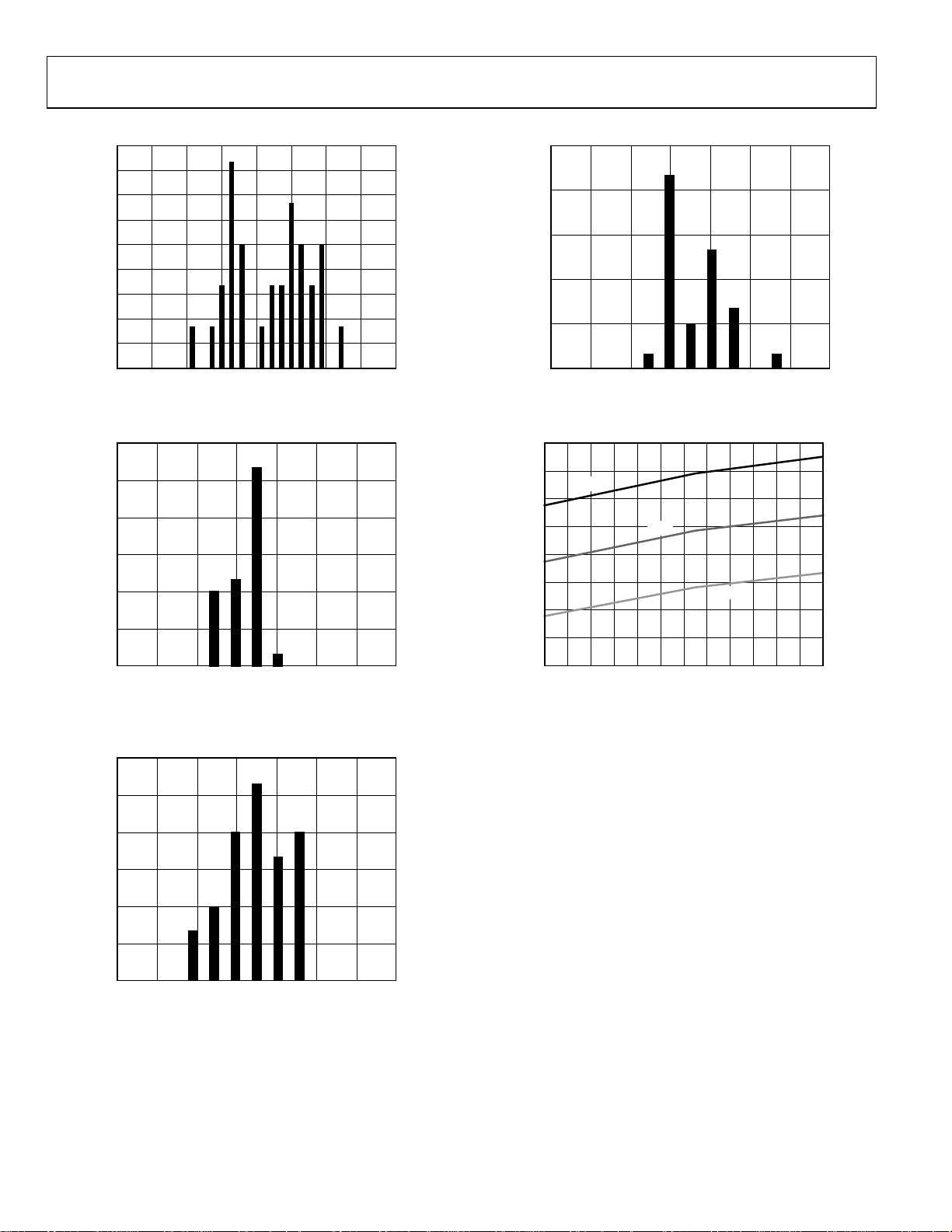
Figure 3. Gain, P1dB, OIP3, and Noise Figure vs. Frequency,
800 MHz to 960 MHz
19.0
18.5
18.0
17.5
17.0
16.5
GAIN (dB)
16.0
15.5
15.0
14.5
14.0
800 820 840 860 880 900 920 940 960
+85°C
FREQUENCY (MHz)
–40°C
+25°C
Figure 4. Gain vs. Frequency and Temperature, 800 MHz to 960 MHz
50
45
OIP3 (+25°C)
40
35
OIP3 (dBm)
30
25
05840-003
20
800 820 840 860 880 900 920 940 960
P1dB (–40 °C)
P1dB (+25°C)
FREQUENCY (MHz )
OIP3 (–40 °C)
OIP3 (+85°C)
P1dB (+85°C)
30
29
28
27
P1dB (dBm)
26
25
05840-006
24
Figure 6. OIP3 and P1dB vs. Frequency and Temperature,
800 MHz to 960 MHz
50
46
42
OIP3 (dBm)
38
34
05840-004
30
Figure 7. OIP3 vs. P
930MHz
880MHz
960MHz
–2 0 2 4 6 8 10121416182022
850MHz
and Frequency, 800 MHz to 960 MHz
OUT
830MHz
P
(dBm)
OUT
05870-007
25.0
–25.5
–26.0
–26.5
–27.0
S12 (dB)
–27.5
–28.0
–28.5
–29.0
700 750 800 850 900 950 1000
S12
S22
S11
FREQUENCY (MHz)
0
–5
–10
–15
–20
–25
–30
–35
–40
Figure 5. Input Return Loss (S11), Output Return Loss (S22), and Reverse
S11 (dB) AND S22 (dB)
05840-005
7.0
6.5
6.0
5.5
5.0
4.5
NF (dB)
4.0
3.5
3.0
2.5
2.0
700 750 800 850 900 950 1000
FREQUENCY (MHz)
+85°C
+25°C
–40°C
05840-008
Figure 8. Noise Figure vs. Frequency and Temperature, 800 MHz to 960 MHz
Isolation (S12) vs. Frequency, 800 MHz to 960 MHz
Rev. 0 | Page 7 of 16

ADL5320
–
45
40
35
30
25
20
15
10
GAIN, NF (dB); P1dB, OIP3 (dBm)
5
0
2060 2080 2100 2120 2140 2160 2180 2200 2220
OIP3 (10dBm)
P1dB
GAIN
NF
FREQUENCY (MHz)
Figure 9. Gain, P1dB, OIP3, and Noise Figure vs. Frequency,
2060 MHz to 2200 MHz
16
15
14
13
GAIN (dB)
12
–40°C
+25°C
+85°C
45
OIP3 (–40 °C)
43
41
39
37
OIP3 (dBM)
35
33
31
05840-009
29
2060 2080 2100 2120 2140 2160 2180 2200 2220
OIP3 (+85°C)
P1dB (–40°C)
P1dB (+25°C)
FREQUENCY (MHz )
OIP3 (+25°C)
P1dB (+85°C)
Figure 12. OIP3 and P1dB vs. Frequency and Temperature,
2060 MHz to 2200 MHz
43
2190MHz
41
39
37
OIP3 (dBm)
35
2060MHz
2090MHz
2220MHz
2140MHz
29.0
28.5
28.0
27.5
27.0
26.5
26.0
25.5
25.0
24.5
P1dB (dBm)
05840-012
11
10
2060 2080 2100 2120 2140 2160 2180 2200 2220
FREQUENCY (MHz)
Figure 10. Gain vs. Frequency and Temperature, 2060 MHz to 2200 MHz
23
–24
S22
–25
S11
–26
S12 (dB)
–27
–28
–29
1900 1950 2000 21002050 2150 2200 2250 230 0
S12
FREQUENCY (MHz)
0
–5
–10
–15
–20
–25
–30
–35
–40
Figure 11. Input Return Loss (S11), Output Return Loss (S22), and Reverse
Isolation (S12) vs. Frequency, 2060 MHz to 2200 MHz
33
05840-010
S11 (dB) AND S22 (dB)
05840-011
31
–2 0 2 4 6 8 10121416182022
Figure 13. OIP3 vs. P
8.0
7.5
7.0
6.5
6.0
5.5
5.0
NF (dB)
4.5
4.0
3.5
3.0
2.5
2.0
1900 1950 2000 2050 2100 2150 2200 2250 2300
P
(dBm)
OUT
and Frequency, 2060 MHz to 2200 MHz
OUT
+85°C
+25°C
–40°C
FREQUENCY (MHz)
05870-013
05840-014
Figure 14. Noise Figure vs. Frequency and Temperature,
2060 MHz to 2200 MHz
Rev. 0 | Page 8 of 16

ADL5320
–
40
35
30
25
20
15
10
GAIN, NF (dB); P1dB, OIP3 (dBm)
5
0
2500 2520 2540 2560 2580 2660 26802600 2620 2640 2700
OIP3 (10dBm)
P1dB
GAIN
NF
FREQUENCY (MHz)
Figure 15. Gain, P1dB, OIP3, and Noise Figure vs. Frequency,
2500 MHz to 2700 MHz
15
05840-015
39
38
OIP3 (–40 °C)
37
36
35
34
OIP3 (dBm)
33
32
31
30
29
2500 2550 2600 2650 2700
OIP3 (+85°C)
P1dB (–40 °C)
P1dB (+25°C)
P1dB (+85°C)
FREQUENCY (MHz)
OIP3 (+25°C)
Figure 18. OIP3 and P1dB vs. Frequency and Temperature,
2500 MHz to 2700 MHz
46
32
31
30
29
28
P1dB (dBm)
27
26
25
05840-018
14
–40°C
13
12
GAIN (dB)
11
10
9
2500 2550 2600 2650 2700
FREQUENCY (MHz)
+25°C
+85°C
Figure 16. Gain vs. Frequency and Temperature, 2500 MHz to 2700 MHz
25.0
–25.5
–26.0
–26.5
–27.0
–27.5
S12 (dB)
–28.0
–28.5
–29.0
–29.5
–30.0
2400 2450 2500 26002550 27002650 2750 2800
FREQUENCY (MHz)
S22
S11
S12
0
–5
–10
–15
–20
–25
–30
–35
–40
44
42
40
(dBm)
2600MHz
2500MHz
05840-019
05840-020
38
OIP3 (dBm)
36
34
32
05840-016
30
–3 –1 1 3 5 7 9 11 13 15 17 19 21 2 3
Figure 19. OIP3 vs. P
8.0
7.5
7.0
6.5
6.0
5.5
5.0
NF (dB)
4.5
S11 (dB) AND S22 (d B)
05840-017
4.0
3.5
3.0
2.5
2.0
2400 2450 2500 2550 2600 2650 2700 2750 2800
2700MHz
P
OUT
and Frequency, 2500 MHz to 2700 MHz
OUT
+85°C
+25°C
–40°C
FREQUENCY (MHz)
Figure 17. Input Return Loss (S11), Output Return Loss (S22), and Reverse
Isolation (S12) vs. Frequency, 2500 MHz to 2700 MHz
Figure 20. Noise Figure vs. Frequency and Temperature,
2500 MHz to 2700 MHz
Rev. 0 | Page 9 of 16
ADL5320
18
16
14
12
10
8
6
PERCENTAGE (%)
4
2
0
42.0 42.8 43. 6 44.4 45.2 46.0 46.8 47.6
OIP3 (dBm)
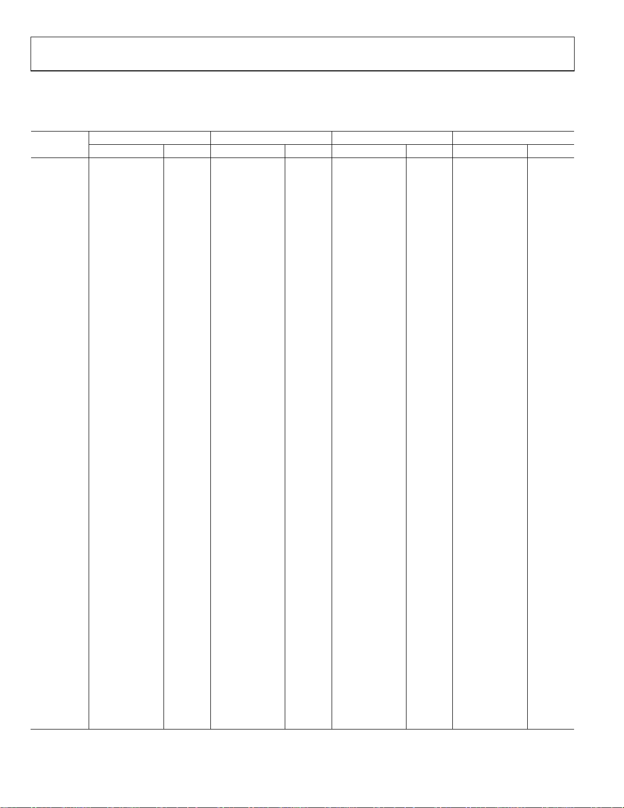
Figure 21. OIP3 Distribution at 880 MHz
60
50
40
30
20
PERCENTAGE (%)
10
0
24.4 24.8 25.2 25.6 26.0 26.4 26. 8
P1dB (dBm)
Figure 22. P1dB Distribution at 880 MHz
50
40
30
20
PERCENTAGE (%)
10
05840-021
0
3.80 3.88 3.96 4.04 4.12 4.20 4. 28
NF (dB)
05840-024
Figure 24. Noise Figure Distribution at 880 MHz
120
115
110
105
100
95
SUPPLY CURRENT (mA)
90
85
05840-022
80
5.25V
5.0V
4.75V
–40 –30 –20 –10 0 10 20 30 40 50 60 70 80
TEMPERATURE ( °C)
05840-025
Figure 25. Supply Current vs. Supply Voltage and Temperature (Using
880 MHz Matching Components)
30
25
20
15
10
PERCENTAGE (%)
5
0
16.65 16.75 16.85 16. 95 17.05 17.15 17.25
GAIN (dB)
05840-023
Figure 23. Gain Distribution at 880 MHz
Rev. 0 | Page 10 of 16

ADL5320
V
BASIC LAYOUT CONNECTIONS
The basic connections for operating the ADL5320 are shown in
Figure 26.
Tabl e 5 lists the required matching components. Capacitors C1,
C2, C3, C4, and C7 are Murata GRM155 series (0402 size) and
Inductor L1 is a Coilcraft 0603CS series (0603 size). For all
frequency bands, the placement of C3 and C7 are critical. From
2300 MHz to 2700 MHz, the placement of C2 is also important.
Tabl e 6 lists the recommended component placement for
various frequencies.
A 5 V dc bias is supplied through L1 which is connected to
RF
(Pin 3). In addition to C4, 10 nF and 10 μF power
OUT
supply decoupling capacitors are also required. The typical
current consumption for the ADL5320 is 110 mA.
SUP
GND
SOLDERING INFORMATION AND RECOMMENDED PCB LAND PATTERN
Figure 27 shows the recommended land pattern for the ADL5320.
To minimize thermal impedance, the exposed paddle on the
SOT-89 package underside is soldered down to a ground plane
along with Pin 2. If multiple ground layers exist, they should
be stitched together using vias. For more information on land
pattern design and layout, refer to the Application Note AN-772,
A Design and Manufacturing Guide for the Lead Frame Chip
Scale Package (LFCSP).
1.80mm
C6 10µF
GND
(2)
C5 10nF
1
C4
5.56mm
0.20mm
3.48mm
ADL5320
1
L1
1
RF
C1
IN
1
SEE TABLE 5 FOR FREQUENCY SPECIFIC COMPONENTS.
2
SEE TABLE 10 FOR RECOMMENDED CO MPONENT SPACING.
IN
2
1
2
λ1
RF
1
C3
3
2
λ3
λ2
OUT
GND
RF
Figure 26. Basic Connections
2
1
C2
2
λ4
1
C7
RF
OUT
05840-026
0.86mm
1.50mm
3.00mm
0.62mm
1.27mm
05840-027
Figure 27. Recommended Land Pattern
Table 5. Recommended Components for Basic Connections
Frequency (MHz) C1 (pF) C2 (pF) C3 (pF) C4 (pF) C7 (pF) L1 (nH)
450 to 500 100 100 18 100 6.8 47
800 to 960 47 47 6.8 100 2.2 47
1805 to 1880 22 22 0.5 22 1.5 15
1930 to 1990 22 22 0.5 22 1.5 15
2110 to 2170 22 22 0.5 22 1.5 15
2300 to 2400 12 2.2 1.2 12 1.0 15
2500 to 2700 12 1.0 1.8 12 0.5 15
Table 6. Matching Component Spacing
Frequency (MHz) λ1 (mils) λ2 (mils) λ3 (mils) λ4 (mils)
450 to 500 391 75 364 50
800 to 960 200 75 100 350
1805 to 2170 300 75 175 275
2300 to 2400 225 75 125 125
2500 to 2700 142 75 89 75
Rev. 0 | Page 11 of 16

ADL5320
MATCHING PROCEDURE
The ADL5320 is designed to achieve excellent gain and IP3
performance. To achieve this, both input and output matching
networks must present specific impedance to the device. The
matching components listed in Tab l e 6 were chosen to provide
−10 dB input return loss while maximizing OIP3. The load-pull
plots (Figure 28, Figure 29, and Figure 30) show the load
impedance points on the Smith chart where optimum OIP3,
gain, and output power can be achieved. These load impedance
values (that is, the impedance that the device sees when looking
into the output matching network) are listed in Tabl e 7 and
Tabl e 8 for maximum gain and maximum OIP3, respectively.
The contours show how each parameter degrades as it is moved
away from the optimum point.
From the data shown in Table 7 and Ta ble 8 it becomes clear that
maximum gain and maximum OIP3 do not occur at the same
impedance. This can also be seen on the load-pull contours in
Figure 28 through Figure 30. Thus, output matching generally
involves compromising between gain and OIP3. In addition,
the load-pull plots demonstrate that the quality of the output
impedance match must be compromised to optimize gain
and/or OIP3. In most applications where line lengths are short
and where the next device in the signal chain presents a low
input return loss, compromising on the output match is
acceptable.
To adjust the output match for operation at a different
frequency or if a different trade-off between OIP3, gain,
and output impedance is desired, the following procedure
is recommended.
For example, to optimize the ADL5320 for optimum OIP3 and
gain at 700 MHz use the following steps:
1. Install the recommended tuning components for a 800 MHz
to 960 MHz tuning band, but do not install C3 and C7.
2. Connect the evaluation board to a vector network analyzer
so that input and output return loss can be viewed simultaneously.
3. Starting with the recommended values and positions for
C3 and C7, adjust the positions of these capacitors along
the transmission line until the return loss and gain are
acceptable. Push-down capacitors that are mounted on
small sticks can be used in this case as an alternative to
soldering. If moving the component positions does not
yield satisfactory results, then the values of C3 and C7
should be increased or decreased (most likely increased
in this case as the user is tuning for a lower frequency).
Repeat the process.
4. Once the desired gain and return loss are realized, OIP3
should be measured. Most likely, it will be necessary to
go back and forth between return loss/gain and OIP3
measurements (probably compromising most on output
return loss) until an acceptable compromise is achieved.
Figure 28. Load-Pull Contours, 880 MHz
Figure 29. Load-Pull Contours, 2140 MHz
Figure 30. Load-Pull Contours, 2600 MHz
5840-028
5840-029
5840-030
Rev. 0 | Page 12 of 16
ADL5320
–
Table 7. Load Conditions for Gain
MAX
ΓLoad
Frequency (MHz)
(Magnitude)
ΓLoad (°) Gain
880 0.5147 159.88 17.76
2140 0.6611 134.40 13.78
2600 0.5835 133.80 12.36
MAX
(dB)
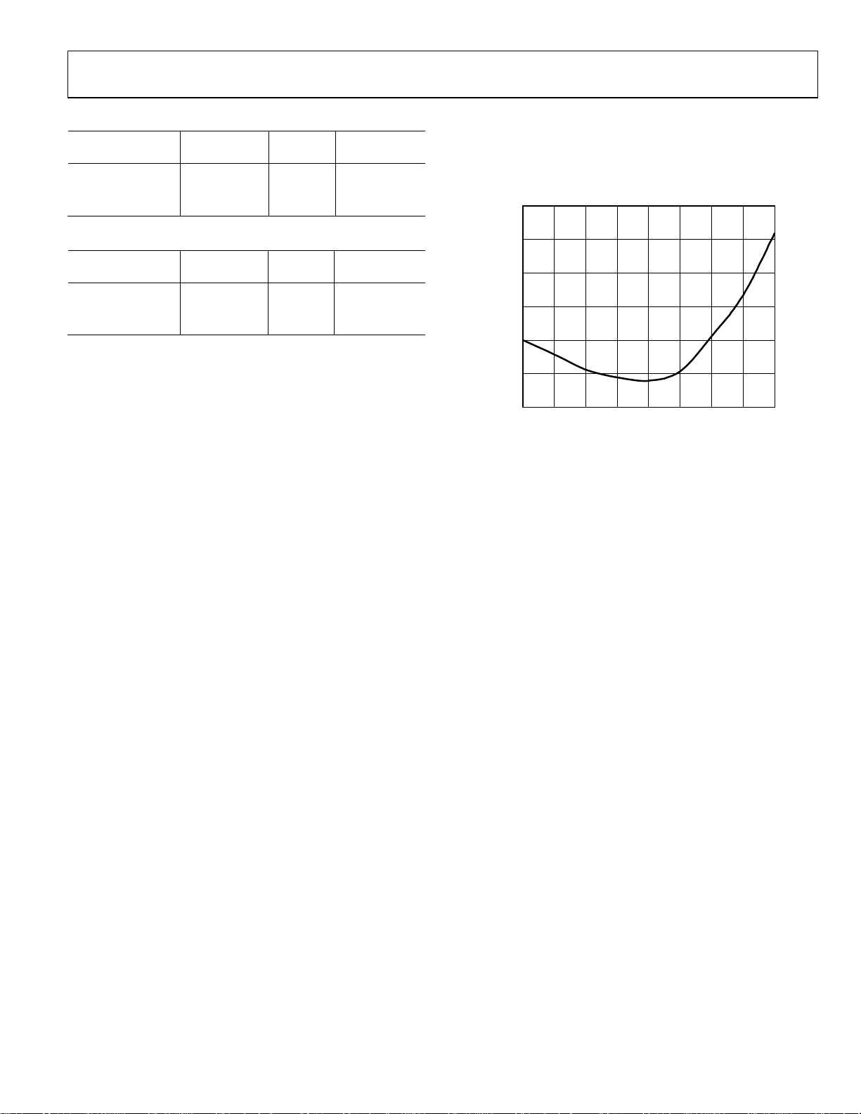
The ADL5320 achieves an ACPR of −82 dBc at 0 dBm output,
at which point device noise and not distortion is beginning to
dominate the power in the adjacent channels. At an output
power of 10 dBm, ACPR is still very low at −70 dBc making the
device particularly suitable for PA driver applications.
30
Table 8. Load Conditions for IP3
MAX
ΓLoad
Frequency (MHz)
(Magnitude) ΓLoad (°) IP3
MAX
(dBm)
880 0.4156 −138.22 46.29
2140 0.5035 +110.27 42.72
2600 0.4595 +102.48 43.01
W-CDMA ACPR PERFORMANCE
Figure 31 shows a plot of adjacent channel power ratio (ACPR)
vs. P
for the ADL5320. The signal type being used is a single
OUT
W-CDMA carrier (Test Model 1−64) at 2140 MHz. This signal
is generated by a very low ACPR source. ACPR is measured at
the output by a high dynamic range spectrum analyzer, which
incorporates an instrument noise correction function.
–40
–50
–60
–70
–80
ACPR @ 5MHz CARRIER OF FSET (d Bc)
–90
–20 –15 –10 –5 0 5 10 15 20
Figure 31. ACPR vs. P
, Single Carrier W-CDMA (Test Model 1−64) at 2140
OUT
P
(dBm)
OUT
MHz Evaluation Board
05840-031
Rev. 0 | Page 13 of 16

ADL5320
V
EVALUATION BOARD
The schematic of the ADL5320 evaluation board is shown in
Figure 32. This evaluation board uses 25 mil wide traces and is
made from FR4 material. The evaluation board comes tuned for
operation in the 1805 MHz to 2140 MHz tuning band. Tuning
options for other frequency bands are also provided in Ta ble 9 .
The recommended placement for these components is provided
in Tabl e 10. The inputs and outputs should be ac-coupled with
appropriately sized capacitors. DC bias is provided to the
amplifier via an inductor connected to the RF
pin. A bias
OUT
voltage of 5 V is recommended.
SUPGND
C6 10µF
C1
22pF
C3
0.5pF
15nH
10uF
10nF
22pF
C7
1.5pF
C2
22pF
GND
(2)
C5 10nF
C4 22pF
ADL5320
L1
C1
RF
22pF
IN
λ1
C3
0.5pF
IN
2
1
RF
3
OUT
GND
RF
15nH
λ3 λ4
λ2
C7
1.5pF
C2
22pF
RF
OUT
05840-032
Figure 33. Evaluation Board Layout and Default Component Placement for
Operation from 1805 MHz to 2170 MHz
Figure 32. Evaluation Board, 1805 MHz to 2170 MHz
Table 9. Evaluation Board Configuration Options
1805 MHz to
2170 MHz
Component Function 450 MHz to 500 MHz 800 MHz to 960 MHz
C1, C2 AC coupling
0402, 100 pF 0402, 47 pF 0402, 22pF C1= 0402 12 pF
Configuration)
capacitors
(Default
C4, C5, C6 Power supply
bypassing
capacitors
L1 DC bias
C4 = 0603 100 pF
C5 = 0603 10 nF
C6 = 1206 10 μF
C4 = 0603 100 pF
C5 = 0603 10 nF
C6 = 1206 10 μF
C4 = 0402 22pF
C5 = 0603 10 nF
C6 = 1206 10 μF
0603, 47 nH 0603, 47 nH 0603, 15 nH 0603, 15 nH 0603, 15 nH
inductor
C3, C7 Tuning
capacitors
C3 = 0402 18 pF
C7 = 0402 6.8 pF
C3 = 0402 6.8 pF
C7 = 0402 2.2 pF
C3 = 0402 0.5 pF
C7 = 0402 1.5 pF
R1 R1 = 0402 0 Ω R1 = 0402 0 Ω
VSUP, GND Power supply
connections
VSUP red test
loop, GND black test
loop
VSUP red test
loop, GND black test
loop
VSUP red test
loop, GND black
test loop
2300 MHz to
2400 MHz
C2 = 0402 2.2 pF
C4 = 0603 12 pF
C5 = 0603 10 nF
C6 = 1206 10 μF
C3 = 0402 1.2 pF
C7 = 0402 1.0 pF
VSUP red test
loop, GND black
test loop
2500 MHz to
2700 MHz
C1 = 0402 12 pF
C2 = 0402 1.0 pF
C4 = 0603 12 pF
C5 = 0603 10 nF
C6 = 1206 10 μF
C3 = 0402 1.8 pF
C7 = 0402 0.5 pF
VSUP red test
loop, GND black
test loop
05840-033
Table 10. Recommended Component Spacing on Evaluation Board
Frequency (MHz) λ1 (mils) λ2 (mils) λ3 (mils) λ4 (mils)
450 to 500 391 75 364 50
800 to 960 200 75 100 350
1805 to 2170 300 75 175 275
2300 to 2400 225 75 125 125
2500 to 2700 142 75 89 75
Rev. 0 | Page 14 of 16

ADL5320
10uF
10nF
C1
100pF
C3
18pF
47nH
100pF
C7
6.8pF
C2
100pF
Figure 34. Evaluation Board Layout and Component Placement
450 MHz to 500 MHz Operation
10uF
10nF
47nH
C7
2.2pF
100pF
C2
47pF
C1
47pF
6.8pF
C3
10uF
10nF
1pF
C7
15nH
12pF
C2
2.2pF
R1 0Ω
05840-035
C1
12pF
05840-037
C3
1.2pF
Figure 36. Evaluation Board Layout and Component Placement
2300 MHz to 2400 MHz Operation
10uF
10nF
C1
12pF
1.8pF
C3
0.5pF
12pF
15nH
C2
1.0pF
R1 0Ω
C7
Figure 35. Evaluation Board Layout and Component Placement
800 MHz to 960 MHz Operation
05840-034
Rev. 0 | Page 15 of 16
05840-036
Figure 37. Evaluation Board Layout and Component Placement
2500 MHz to 2700 MHz Operation

ADL5320
OUTLINE DIMENSIONS
*
1.55 REF
4.25
3.94
1.50 TYP
(2)
12
3.00 TYP
4.60
4.40
*
0.58
0.40
*
COMPLIANT TO JEDEC STANDARDS TO-243 W ITH
EXCEPTIO N TO DIMENSIONS INDICAT ED BY AN ASTERISK.
2.60
2.30
3
1.20
0.90
0.44
0.35
*
0.52
0.32
END VIEW
1.60
1.40
040407-A
Figure 38. 3−Lead Small Outline Transistor Package [SOT-89]
(RK-3)
Dimensions shown in millimeters
ORDERING GUIDE
Model Temperature Range Package Description Package Option
ADL5320ARKZ-R7
ADL5320-EVALZ
1
Z = RoHS Compliant Part.
1
−40°C to +85°C 3-Lead SOT-89, 7“ Tape and Reel RK-3
1
Evaluation Board
©2008 Analog Devices, Inc. All rights reserved. Trademarks and
registered trademarks are the property of their respective owners.
D05840-0-2/08(0)
Rev. 0 | Page 16 of 16
 Loading...