

Avalanche Photodiode Bias Controller and
Wide-range (5 nA - 5 mA) Current Monitor
PRELIMINARY TECHNICAL DATA
FEATURES
Accurately sets avalanche photodiode bias voltage
Wide bias range from 6 V to 75 V set
Using 3V-compatible control interface
Monitors photodiode current (5:1 ratio) over 6 decades
Linearity 0.5% from 10 nA to 1 mA, 1% from 5 nA to 5 mA
Over-current protection and over-temperature shutdown
Miniature 16-lead chip scale package (LFCSP 3 mm × 3 mm)
APPLICATIONS
Optical power monitoring and biasing in APD systems
Wide dynamic range voltage sourcing and current
monitoring in high-voltage systems
GENERAL DESCRIPTION
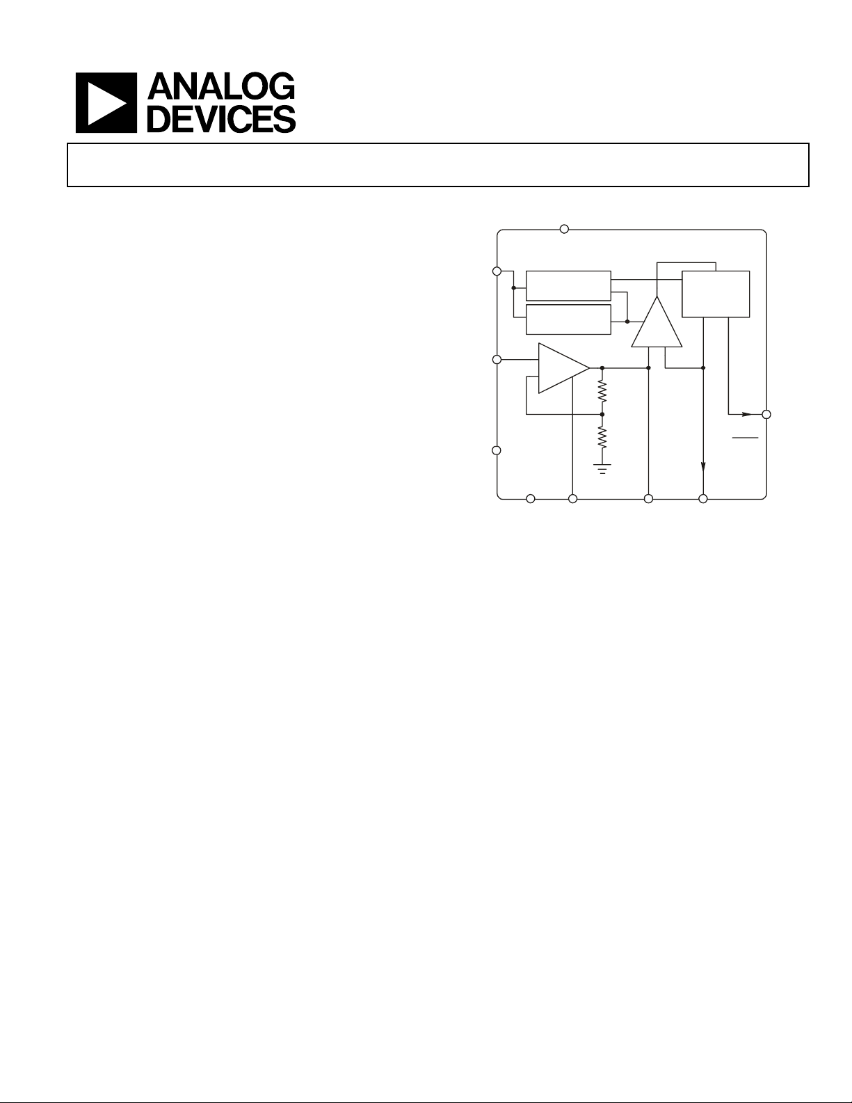
The ADL5317 is a high-voltage, wide dynamic range biasing and
current monitoring device optimized for use with avalanche
photodiodes. With the provision of a stable high-voltage supply up
to 80 V, the bias voltage at the VAPD pin can be varied from 6 V to
75 V using the 3 V-compatible VSET pin. The current sourced
from the VAPD pin, over a range of 5 nA to 5 mA, is accurately
mirrored with an attenuation of 5 and sourced from the IPDM
monitor output. In a typical application, the monitor output drives
a current-input logarithmic amplifier to produce an output
representing the optical power incident upon the photodiode. The
photodiode anode may be connected to a high-speed
transimpedance amplifier for the extraction of the data stream.
A signal applied at the VSET pin of 0.2 V to 2.5 V with respect to
COMM is amplified by a fixed gain of 30 to produce the 6 V to 75 V
bias at pin VAPD. The accuracy of the ADL5317’s bias control
interface allows for straightforward calibration to maintain
constant avalanche multiplication factor of the photodiode over
temperature. The current monitor output, IPDM, maintains its high
linearity versus photodiode current over the full range of APD bias
voltage. The current ratio of 5:1 remains constant as VSET and
VPHV are varied.
ADL5317
FUNCTIONAL BLOCK DIAGRAM
COMM
FALT
Overcurrent
Protection
Thermal
Protection
VSET
+
30 V
-
VPLV
VPHV VCL H
Figure 1. Functional Block Diagram
The ADL5317 also offers a supply tracking mode for compatibility
with adjustable high voltage supplies. The VAPD pin accurately
follows 2.0 V below the VPHV supply pin when VSET is tied to a
voltage from 3 V to 5.5 V (or higher with current limiting resistor)
and the VCLH pin is open.
Protection from excessive input current at VAPD and excessive die
temperature is provided. The voltage at VAPD falls rapidly from its
setpoint when the input current exceeds 18 mA nominally. A die
temperature in excess of 140°C will cause the bias controller and
monitor to shut down until the temperature falls below 120°C.
Either overstress condition will trigger a logic low at the FALT pin,
an open-collector output loaded by an external pull-up to an
appropriate logic supply (1 mA max.).
The ADL5317 is available in a 16-lead LFCSP package and is
specified for operation from −40°C to +85°C.
.
29 R
R
+
SET
.
GARD VAPD
Current
Mirror
5:1
-
IPDM
I
APD
5
I
APD
Rev. PrE
Information furnished by Analog Devices is believed to be accurate and reliable.
However, no responsibility is assumed by Analog Devices for its use, nor for any
infringements of patents or other rights of third parties that may result from its use.
Specifications subject to change without notice. No license is granted by implication
or otherwise under any patent or patent rights of Anal og Devices. Trademarks and
registered trademarks are the property of their respective companies.
One Technology Way, P.O. Box 9106, Norwood, MA 02062-9106, U.S.A.
Tel: 781.329.4700 www.analog.com
Fax: 781.326.8703 © 2005 Analog Devices, Inc. All rights reserved.

ADL5317 PRELIMINARY TECHNICAL DATA
Rev. PrE | Page 2 of 11
ADL5317—Specifications
Table 1. V
= 78 V, V
PHV
PLV
= 5 V, I
= 5 µA, TA = 25°C, unless otherwise noted
APD
Parameter Conditions Min Typ Max Unit
CURRENT MONITOR OUTPUT
Current Gain from VAPD to IPDM
Wideband Noise at IPDM
APD BIAS CONTROL
Voltage Range of V
APD
Specified Input Current Range, I
Incremental Gain from VSET to VAPD
VSET Voltage Range
Incremental Input Resistance at VSET
Input Bias Current at VSET
V
Settling Time, 5%
APD
V
Supply Tracking Offset (below V
APD
OVERSTRESS PROTECTION
VAPD Current Compliance Limit
APD
IPDM (Pin 11)
−40°C < TA < +85°C
10 nA < I
5 nA < I
I
= 5 nA 2 kHz Small-signal Bandwidth
APD
I
= 5 µA
APD
I
= 5 µA, C
APD
V
APD
V
APD
< 1 mA 0.5 TBD % Nonlinearity
APD
< 5 mA 1 TBD %
APD
= 1 nF
GRD
> 3 V
PLV
< 3 V
PLV
VSET (Pin 2), VAPD (Pin 8)
10 V < V
41 V < V
76.5V < V
< 41 V 6 V
PHV
< 76.5 V V
PHV
< 80 V V
PHV
Flows from VAPD pin
0.2 V < V
< 2.4 V TBD 30 TBD V/V
SET
0.2 5.5 V
V
= 2.0 V 50 MOhms
SET
V
= 2.0 V 0.3
SET
V
PHV
) V
= 1.6 V to 2.4 V, C
SET
V
= 2.4 V to 1.6 V, C
SET
= 5.0 V, 10 V < V
SET
= 1 nF 20
GRD
= 1 nF 150
GRD
< 77 V TBD 2.0 TBD V
PHV
FALT (Pin 1)
V
= 2.0 V, V
SET
deviation of 500 mV TBD 18 TBD mA
APD
Thermal Shutdown Trip Point Die temperature rising 140
Thermal Hysteresis 20
FALT Output Low Voltage
POWER SUPPLIES
Low Voltage Supply
Quiescent Current Independent of I
High Voltage Supply
Quiescent Current
I
Fault condition, Load current < 1 mA 0.8 V
VPHV (Pin 4, 5), VPLV (Pin 3)
VPLV
APD
VPHV
= 5 µA, V
I
APD
= 1 mA, V
APD
=60 V
APD
= 60 V 3.3 TBD mA
APD
TBD 0.200 TBD A/A
2 MHz
13 nArms
0 V
0 V
PLV
APD
V Output Voltage Range
/ 3 V
–1.5 V
PHV
–35 V
PHV
–35 75 V
PHV
–1.5 V
PHV
5n 5m A
µA
µsec
µsec
°C
°C
4 6 V
0.7 TBD mA
10 80 V
2.0 TBD mA
ADL5317 PrE 02/27/2005

PRELIMINARY TECHNICAL DATA ADL5317
Rev. PrE | Page 3 of 11
ABSOLUTE MAXIMUM RATINGS
Table 2. ADL5317 Absolute Maximum Ratings
Parameter Rating
Supply Voltage
Input Current at VAPD
Internal Power Dissipation
θ
(soldered exposed paddle)
JA
Maximum Junction Temperature
Operating Temperature Range
Storage Temperature Range
Lead Temperature Range (Soldering 60 sec)
80 V
25 mA
615 mW
65°C/W
125°C
–40°C to +85°C
–65°C to +150°C
300°C
Stresses above those listed under Absolute Maximum Ratings
may cause permanent damage to the device. This is a stress
rating only; functional operation of the device at these or any
other conditions above those indicated in the operational
section of this specification is not implied. Exposure to absolute
maximum rating conditions for extended periods may affect
device reliability.
ADL5317 PrE 02/27/2005
ADL5317 PRELIMINARY TECHNICAL DATA
Rev. PrE | Page 4 of 11
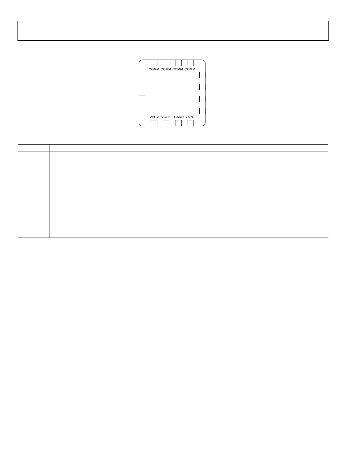
PIN CONFIGURATION AND FUNCTIONAL DESCRIPTIONS
14
16
15
13
Table 3. Pin Function Descriptions
Pin No. Mnemonic Function
1
2
3
4, 5
6
7,9
FALT
VSET
VPLV
VPHV
VCLH
GARD
Indicates over-current or over-temperature condition. Open collector; active low.
APD Bias Voltage Setting Input. Short to VPLV for supply tracking mode.
Low Voltage Supply, 4 V to 6 V
High Voltage Supply, 10 V to 80 V.
May be shorted to VPHV for extended linear operating range. No connect for supply tracking mode.
Guard pin tracks VAPD pin and filters setpoint buffer noise (with extenal capacitor C
shielding of VAPD trace. Capacitive load only.
8
10
11
12
13–16
VAPD
N/C
IPDM
N/C
COMM
APD Bias Voltage Output and Current Input. Sources current only.
Optional shielding of IPDM trace. No connection to die.
Photodiode Monitor Current Output. Sources current only. Current at this node is equal to I
Optional shielding of IPDM trace. No connection to die.
Analog Ground.
1
FALT
2
VSET
ADL5317
3
VPLV
4
VPHV
6
5
Figure 2. 16-Lead Leadframe Chip Scale Package (LFCSP)
7
N/C
IPDM
N/C
GARD
8
12
11
10
9
to COMM). Optional
GRD
/5.
APD
ADL5317 PrE 02/27/2005

PRELIMINARY TECHNICAL DATA ADL5317
Rev. PrE | Page 5 of 11
TYPICAL PERFORMANCE CHARACTERISTICS
(V
= 75 V, V
PHV
1.E-02
1.E-03
VPHV = 75V, VAPD = 60V
VPHV = 60V, VAPD = 45V
VPHV = 30V, VAPD = 25V
= 60 V, TA = 25°C, unless otherwise noted.)
APD
80
70
VPHV = 75V
1.E-04
1.E-05
1.E-06
IPDM - Amperes
1.E-07
1.E-08
1.E-09
1.E-10
1.E-09 1.E-08 1.E-07 1.E-06 1.E-05 1.E-04 1.E-03 1.E-02
Figure 3. I
5
4
VPHV = 75V, VAPD = 60V
3
VPHV = 60V, VAPD = 45V
2
1
0
Error - %
-1
VPHV = 30V, VAPD = 25V
-2
-3
-4
-5
1.E-09 1.E-08 1.E-07 1.E-06 1.E-05 1.E-04 1.E-03 1.E-02
Figure 4. I
APD
Error vs. I
PDM
vs. I
Normalized to I
IAPD - Amperes
for Multiple Values of V
PDM
IAPD - Amperes
for Multiple Values of V
APD
= 10 µA, VPHV = 75V, VAPD = 60V
APD
APD
and V
and V
APD
PHV
PHV
,
60
50
VPHV = 75V
40
VAPD - Volts
30
VPHV = 60V
20
10
0
0 0.5 1 1.5 2 2.5 3
Figure 5. V
70
60
VPHV = 75V, VAPD = 60V
50
VPHV = 60V, VAPD = 45V
40
30
VAPD - Volts
VPHV = 30V, VAPD = 25V
20
10
0
1.E-09 1.E-08 1.E-07 1.E-06 1.E-05 1.E-04 1.E-03 1.E-02
Figure 6. V
and Normalized V
APD
VPHV = 12V
V
VPHV = 30V
vs. V
APD
SET
VPHV = 30V, VAPD = 25V
IAPD - Amperes
APD
Normalized to I
APD
VSET - Volts
(I
= 5 µA, VCLH open)
APD
vs. I
APD
VPHV = 60V
0.03
0.02
VPHV = 75V, VAPD = 60V
VPHV = 60V, VAPD = 45V
0.01
0
-0.01
Normalized VAPD - Volts
-0.02
-0.03
-0.04
for Multiple Supply Conditions,
= 10 µA
APD
ADL5317 PrE 02/27/2005

ADL5317 PRELIMINARY TECHNICAL DATA
Rev. PrE | Page 6 of 11
GENERAL STRUCTURE
The ADL5317 is designed to address the need for high voltage
bias control and precision optical power monitoring in optical
systems utilizing avalanche photodiodes. It is optimized for use
with ADI’s family of translinear logarithmic amplifiers to make
the best use of its wide input current range. This arrangement
allows the anode of the photodiode to be connected directly to a
transimpedance amplifier for the extraction of the data stream
without the need for a separate optical tap for power
monitoring. The basic connections for the ADL5317 are shown
in Figure 7.
14
13
12
N/C
IPDM
11
N/C
10
GARD
8
7
1kΩ
0.01µF
9
1nF
FALT
Low Voltage
Supply
0.1µF
10kΩ
1516
1
FALT
V
SET
0Ω
2
VSET
3
VPLV
0.01µF
4
VPHV
5
0.01µF
0Ω
0.1µF
High Voltage
Supply
Figure 7: Basic Connecti ons
ADL5317
6
At the heart of the ADL5317 is a precision attenuating current
mirror with a voltage following characteristic that provides
precision biasing at the monitor input. This architecture uses a
JFET-input amplifier to drive the bipolar mirror and maintain
stable VAPD voltage while offering very low leakage current at
the VAPD pin. The mirror attenuates the current sourced
through VAPD by a factor of 5 to limit power dissipation under
high-voltage operation and delivers the mirrored current to the
IPDM monitor output pin. Proprietary mirroring and
cascoding techniques maintain the linearity vs. input current
and stability of attenuation over a very wide range of supply and
VAP D v ol ta ge s.
BIAS CONTROL INTERFACE
In the linear operating mode, the voltage at VAPD is referenced
to COMM, and follows the equation:
VV ⋅= 30
SETAPD
GARD is driven to the same potential as VAPD for use in
shielding the highly sensitive VAPD pin from leakage currents.
The GARD and VAPD pins are clamped to within
approximately 40 V below the VPHV supply to prevent internal
device breakdowns, and VAPD is clamped to within a volt of
GARD.
The VAPD adjustment range for a given VPHV voltage is
limited to approximately 33 V (or less, for VPHV < 41 V). For
example, VAPD is specified from 40 V to 73.5 V for a 75 V
supply, and 6 V (the minimum allowed) to 28.5 V for a 30 V
supply. When VAPD is driven to its lower clamp voltage via the
VSET pin, the mirror continues to operate, but the APD bias
voltage no longer responds to incremental changes in V
SET
.
GARD INTERFACE
GARD is driven by the VSET amplifier through a 20 kΩ resistor.
This resistor forms an RC network with an external capacitor
from GARD to ground which filters the thermal noise of the
amplifier’s feedback network as well as provides additional
power supply rejection. A larger value of external capacitor (up
to approx. 0.01uF) will provide superior noise performance at
the lowest input current levels, but will slow the response time
to changes in V
. Any DC load on GARD will alter the gain
SET
from VSET to VAPD (due to the 20 kΩ source impedance).
Note that the load presented by a multimeter or oscilloscope
probe is sufficient to alter the VSET to VAPD gain and must be
taken into account.
The GARD pin is internally clamped to approximately 40 V
below VPHV to prevent device breakdown, and VAPD is
clamped to within a volt of GARD. For this reason, any short
circuit to ground from GARD or VAPD must be avoided for
VPHV voltage above 36 V or device damage will result.
VCLH INTERFACE
The VCLH pin (Voltage CLamp High-side) is typically
connected to VPHV for linear operation of the VSET interface
and left open for supply tracking mode (see Applications for
more details on supply tracking mode). The voltage at VCLH
represents a high-side clamp above which the VSET amplifier
output (and VAPD) is not allowed to rise. The voltage is
internally set to a temperature-stable 2.0 V below VPHV
through a 25 kΩ resistor. When V
higher and VCLH is open, therefore, VAPD follows 2.0 V below
VPHV as VPHV is varied. This bypasses the linear VSET
interface for applications where an adjustable high-voltage
supply is preferred (see Applications). The 25 kΩ source
resistance allows VCLH to be shorted to VPHV, removing the
2.0 V high-side clamp for extended linear operating range (up
to VPHV – 1.5 V over all conditions) in linear mode. VCLH
may be left open in linear mode as well if a fixed clamp point is
desired.
is pulled up to 3 V or
SET
ADL5317 PrE 02/27/2005

PRELIMINARY TECHNICAL DATA ADL5317
Rev. PrE | Page 7 of 11
NOISE PERFORMANCE
Noise performance for the ADL5317 is defined as the RMS
noise current as a fraction of the output DC current. The
amount of noise generated by the ADL5317 improves with
increasing signal current. This partially results from the
relationship between quiescent collector current and shot noise
in bipolar transistors. At lower signal current levels, the noise
contribution from the V
amplifier and other noise sources
SET
appearing at VAPD dominate the noise behavior. Filtering the
VSET interface noise through an external capacitor from GARD
to ground, as well as selecting optimal external compensation
components on VAPD, minimizes the amount of voltage noise
at VAPD that will be converted to current noise at IPDM.
RESPONSE TIME
The response time for changes in signal current is
fundamentally a function of signal current, with small-signal
bandwidth increasing roughly in proportion to signal current.
The value of the external compensating capacitor on VAPD
strongly impacts response time; however, the value must be
chosen to maintain stability and prevent noise peaking.
DEVICE PROTECTION
Thermal and over-current protection are provided with fault
detection. The FALT pin is an open collector logic output
(active low) designed to assert when an over-temperature or
over-current condition is detected. A pull-up resistor to an
appropriate logic supply is required, and its value should be
chosen such that 1 mA maximum output current is used when
active.
When the die temperature of the ADL5317 exceeds 140°C
(typical), the current mirror will shut down, allowing VAPD to
be pulled down, and FALT will assert. FALT will remain
asserted until the temperature falls below the trigger
temperature minus the thermal hysteresis (20°C typical), after
which the mirror and biaser will again power up. The cycle may
repeat until the cause of the fault is removed.
When the input current exceeds 18 mA (typical), the current
mirror and biaser will attempt to maintain the threshold current
by allowing the VAPD voltage to fall to a point of equilibrium.
In other words, the threshold current represents the compliance
of the bias voltage, in this case the current at which VAPD falls
500 mV below its mid-range current value. FALT will assert,
but it is not guaranteed to remain asserted as VAPD is pulled
down toward ground. If VAPD falls below ~3 V, as in the case
of a momentary short circuit or being driven by a
programmable current source exceeding the threshold current,
bias current generators critical to device operation will become
saturated, causing FALT to de-assert and the mirror to shut
down. The mirror will not power up until the input current
falls below the current limit of the VSET amplifier
(approximately 2.5 mA), allowing VAPD to be pulled up to its
normal operating level.
The FALT pin may be grounded or tied to VPLV if the logic
signal is not used.
ADL5317 PrE 02/27/2005

ADL5317 PRELIMINARY TECHNICAL DATA
Rev. PrE | Page 8 of 11
APPLICATIONS
The ADL5317 Avalanche Photodiode Bias Controller and
Current Mirror is primarily designed for wide-dynamic range
applications simplifying APD bias circuit architecture. Accurate
control of the bias voltage across the APD becomes critical in
order to maintain the proper avalanche multiplication factor as
the temperature and input power vary. Figure 8 shows how the
ADL5317 can be used with an external temperature sensor to
monitor the ambient temperature of the APD, and then using a
look-up table and DAC to drive VSET, apply the correct V
APD
for
the conditions.
LOGIC
SUPPLY
LOOK−UP
TABLE
AND DAC
5 V
COMM
FALT
OVERCURRENT
PROTECTION
PROTECTION
VSET
VPLV
VPHV
75 V
From DC−DC
Converter
THERMAL
+
−
30*V
SET
29R
R
VCLH
TEMPERATURE
SENSOR
+
GARD
−
CURRENT
MIRROR
5 : 1
I
APD
VAPD
APD
IPDM
I
APD
LOG AMP
−
+
5
−
+
TIA
DATA
OPTICAL
POWER
Figure 8: Typical APD Biasing Application using the ADL5317
In this application the ADL5317 is operating in it’s linear mode.
The bias voltage to the APD at pin VAPD is controlled by the
voltage (V
30*V
) at pin VSET. The bias voltage at VAPD is equal to
SET
.
SET
The range of voltages available at VAPD for a given high voltage
supply is limited to approximately 33 V (or less, for
VAPD < 41 V). This is because the GARD and VAPD pins are
clamped to within ~40 V below VPHV, preventing internal
device breakdowns
The input current I
is divided down by a factor of 5 and
APD
precisely mirrored to pin IPDM. This interface is optimized for
use with any of ADI’s translinear logarithmic amplifiers
(AD8304, AD8305, etc.) to offer a precise, wide-dynamic range
measurement of the incident optical power across the APD.
If a voltage output is preferred at IPDM a single external resistor
to ground is all that is necessary to perform the conversion.
Voltage compliance at IPDM is limited to VPLV.
SUPPLY TRACKING MODE
Some applications for the ADL5317 may require a variable
DC-DC converter or alternative variable biasing sources to
supply VPHV. For such applications it is necessary to configure
the ADL5317 for Supply Tracking Mode, shown in Figure 9. In
this mode the V
functionality of the precision current mirror remains available.
In supply tracking mode the VSET amplifier is pulled up
beyond its linear operating range and effectively placed into a
controlled saturation. This is done by applying 3 V to 5.5 V at
the VSET pin. It is also necessary to remove the connection
from VCLH (which defines the saturation point) to VPHV.
Once the ADL5317 is placed into supply tracking mode VAPD
is clamped to 2.0V below VPHV.
For those designs where it is desirable to drive VSET and VPLV
from the same supply it is necessary to place a 100 kΩ resistor
between VSET and VPLV for voltages >5.5 V. This is due to the
input current limitations on the VSET pin.
interfaced is bypassed, however the full
SET
Figure 9: Supply Tracking Mode
ADL5317 PrE 02/27/2005

ADL5317 PRELIMINARY TECHNICAL DATA
Rev. PrE | Page 9 of 11
EVALUATION BOARD
Table 4: Evaluation Board Configuration Options
Component Function Default Condition
VPHV, VPLV, GND
VSET
R11, C8
VAPD, L1, C9
IPDM, R1
R7, R8, R9, R10, C6,
C7, C10
VPLV, W2, R3
VCLH, W1, C4, R6
FALT, R2
C1, C2, C3, C5, R4,
R5
High and Low Voltage Supply and Ground Pins
APD Bias Voltage Setting Pin. The dc voltage applied to VSET
determines the APD bias voltage at VAPD. VAPD = 30*VSET.
APD Input Compensation. Provides essential HF compensation at the
VAPD input pin.
Input Interface. The evaluation board is configured to accept an input
current at the SMA connector labeled VAPD. Filtering of this current can
be done using L1 and C9.
Mirror Interface. The output current at the SMA connector labeled IPDM
is 1/5 the value at VAPD. R1 allows a resistor to be installed for
applications where a scaled voltage referenced to I
of a current.
Guard Options. By populating R9 and/or R10 the shell of the VAPD SMA
connector is set to the GARD potential. R7 and R8 are installed so that the
guard potential can be driven by an external source, such as the VSUM
potential of Analog Devices’ Optical log amps. C7 filters noise from the
VSET interface as well as provides a high frequency AC path to ground.
Additional filtering is possible by installing a capacitor at C10. C10 should
equal C7.
Optional Supply Tracking Mode. Connecting jumper W2 and opening
W1 places the ADL5317 into supply tracking mode. In this mode the
voltage at VAPD is typically 2V below VPHV. R3 = 100 kΩ for VPLV > 5.5 V.
Extended Linear Operating Range. Closing W1 connects pins VPHV and
VCLH. This allows for an extended linear control range of VAPD using
VSET.
FALT Int erfac e. R2 is a resistive pull-up that is used to create the logic
signal at FALT.
Supply Filtering/Decoupling
is desirable instead
APD
Not Applicable
Not Applicable
C8 = 1 nF (size 0805)
R11 = 1 kΩ (size 0402)
L1 = 0 Ω (size 0805)
C9 = open (size 0805)
R1 = open (size 1206)
R7 = R8 = 0 Ω (size 0402)
R9 = R10 = open (size 0402)
C7 = 0.01 µF (size 0402)
C6 = C10 = open (size 0402)
R3 = 0 Ω (size 0402)
W1 = open
W2 = closed
W1 = closed
C4 = open (size 0402)
R6 = 0 Ω (size 0402)
R2 = 10 kΩ (size 0402)
C1 = C2 = 0.01 µF (size 0402)
C3 = C5 = 0.1 µF (size 0603)
R4 = R5 = 0 Ω (size 0402)
ADL5317 PrE 02/27/2005

ADL5317 PRELIMINARY TECHNICAL DATA
Rev. PrE | Page 10 of 11
14
1516
13
FALT
VSET
VPLV
10kΩ
C3
0.1µF
GND
1
FALT
2
VSET
R3
R4
0Ω
W2
0Ω
C2
0.01µF
C1
0.01µF
C5
0.1µF
VPHV
3
VPLV
4
VPHV
R5
0Ω
R2
5
W1
ADL5317
6
7
R6
0Ω
C4
open
C10
open
R10
open
L1
0Ω
N/C
IPDM
N/C
GARD
8
R11
1kΩ
C9
open
12
11
10
9
C8
1nF
C7
0.01µF
R9
open
C6
open
R1
open
R8
0Ω
R7
0Ω
Figure 10: ADL5317 Evaluation Board Schematic
ADL5317 PrE 02/27/2005
Figure 11: ADL5317 Evaluation Board Layout
Figure 12: ADL5317 Evaluation Board Silkscreen

PRELIMINARY TECHNICAL DATA ADL5317
Rev. PrE | Page 11 of 11
PR05456-0-2/05(PrE)
2005
OUTLINE DIMENSIONS
BOTTOM
VIEW
0.50
0.40
0.30
PIN 1 INDICA
1
2
1.45
SQ
1.30
1.15
0.25 MIN
TO R
3.00
BSC SQ
PIN 1
INDICATOR
1.00
0.90
0.80
SEATING
PLANE
TOP
VIEW
12 ° MAX 0.80 MAX
0.30
0.23
0.18
2.75
BSC SQ
0.65 NOM
0.20 REF
0.05 MAX
0.01 NOM
Figure 13. 16-Lead Lead Frame Chip Scale Package
0.45
0.50
BSC
1.50 REF
0.60 MAX
ESD CAUTION
ESD (electrostatic discharge) sensitive device. Electrostatic charges as high as 4000 V readily accumulate on the
human body and test equipment and can discharge without detection. Although the ADL5317 features
proprietary ESD protection circuitry, permanent damage may occur on devices subjected to high energy
electrostatic discharges. Therefore, proper ESD precautions are recommended to avoid performance
degradation or loss of functionality.
Table 5. Ordering Guide
ADL5XXX Products Temperature Package Package Description Package Outline Branding
ADL5317XCP –40°C to +85°C 16-Lead LFCSP CP-16
ADL5317-EVAL Evaluation Board
© 2004 Analog Devices, Inc. All rights reserved. Trademarks and
registered trademarks are the property of their respective companies.
ADL5317 PrE 02/27/2005
 Loading...