120 dB Range (3 nA to 3 mA)
FEATURES
2 independent channels optimized for photodiode
interfacing
6-decade input dynamic range
Law conformance 0.3 dB from 3 nA to 3 mA
Temperature-stable logarithmic outputs
Nominal slope 10 mV/dB (200 mV/dec), externally scalable
Intercepts may be independently set by external resistors
User-configurable output buffer amplifiers
Single- or dual-supply operation
Space-efficient, 24-lead 4 mm × 4 mm LFCSP
Low power: < 10 mA quiescent current
APPLICATIONS
Gain and absorbance measurements
Multichannel power monitoring
General-purpose baseband log compression
PRODUCT DESCRIPTION
The ADL53101 low cost, dual logarithmic amplifier converts
input current over a wide dynamic range to a linear-in-dB
output voltage. It is optimized to determine the optical power
in wide-ranging optical communication system applications,
including control circuitry for lasers, optical switches, attenuators, and amplifiers, as well as system monitoring. The device
is equivalent to a dual AD8305 with enhanced dynamic range
(120 dB). While the ADL5310 contains two independent signal
channels with individually configurable transfer function
constants (slope and intercept), internal bias circuitry is shared
between channels for improved power consumption and
channel matching. Dual converters in a single, compact LFCSP
package yield space-efficient solutions for measuring gain or
attenuation across optical elements. Only a single supply is
required; optional dual-supply operation offers added flexibility.
Dual Logarithmic Converter
ADL5310
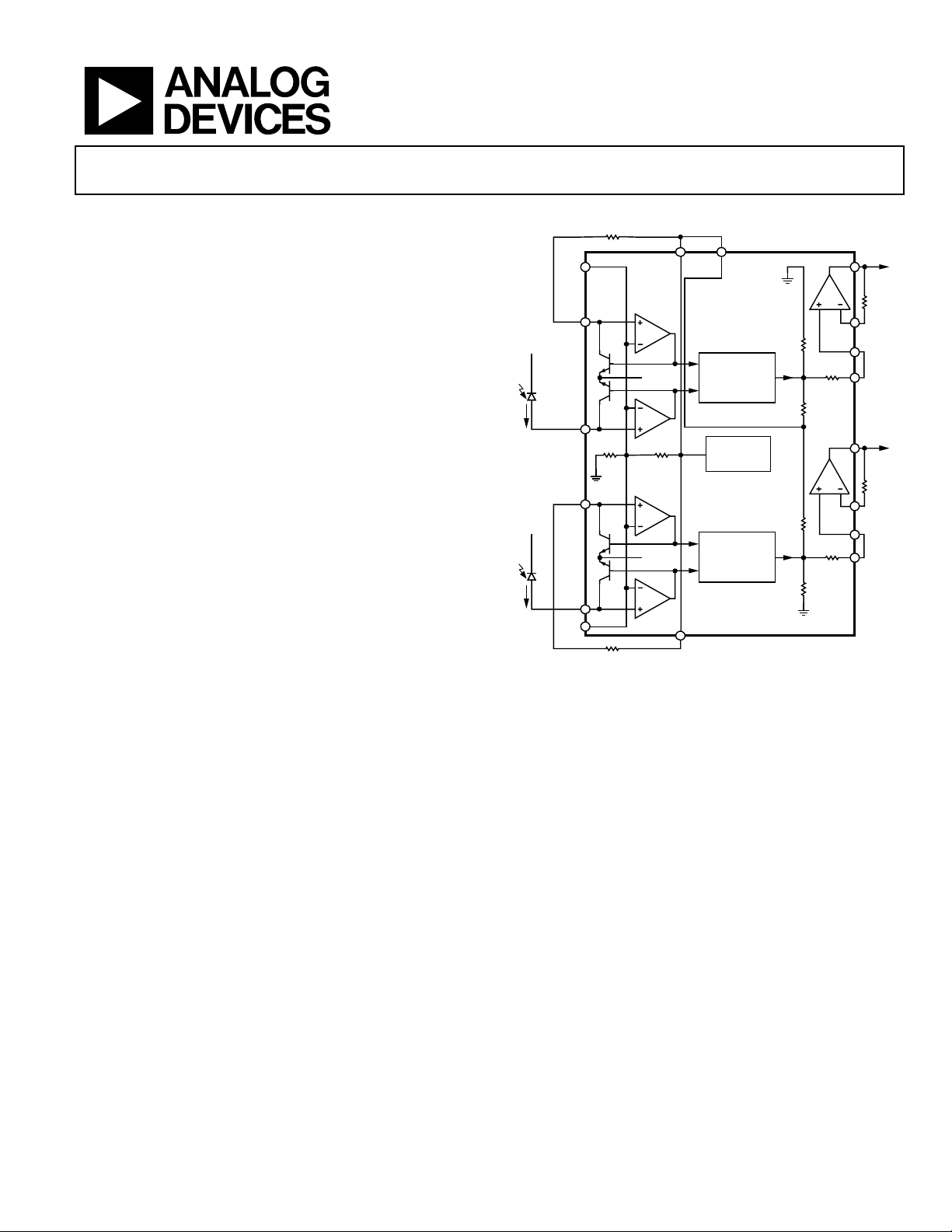
FUNCTIONAL BLOCK DIAGRAM
665kΩ
VSUM
IRF1
V
BIAS
INP1
I
PD1
COMM
IRF2
V
BIAS
INP2
I
PD2
VSUM
665kΩ
The logarithmic slope is set to 10 mV/dB (200 mV/decade)
nominal and can be modified using external resistors and the
independent buffer amplifiers. The logarithmic intercepts for
each channel are defined by the individual reference currents,
which are set to 3 μA nominal for maximum input range by
connecting 665 kΩ resistors between the 2.5 V VREF pins and
the IRF1 and IRF2 inputs. Tying VRDZ to VREF effectively sets
the x-intercept four decades below the reference current—
typically 300 pA for a 3 µA reference.
VREF VRDZ
VNEG
2.5V0.5V
80kΩ20kΩ
VNEG
VREF
Figure 1.
COMM
TEMPERATURE
COMPENSATION
REFERENCE
GENERATOR
TEMPERATURE
COMPENSATION
6.69kΩ
I
LOG
14.2kΩ
14.2kΩ
I
LOG
6.69kΩ
COMM
451Ω
451Ω
OUT1
V
SCL1
BIN1
LOG1
OUT2
V
SCL2
BIN2
LOG2
OUT1
4.99kΩ
OUT2
4.99kΩ
04415-0-001
The ADL5310 employs an optimized translinear structure that
use the accurate logarithmic relationship between a bipolar
transistor’s base emitter voltage and collector current, with
appropriate scaling by precision currents to compensate for the
inherent temperature dependence. Input and reference current
pins sink current ranging from 3 nA to 3 mA (limited to ±60 dB
between input and reference) into a fixed voltage defined by the
VSUM potential. The VSUM potential is internally set to
500 mV but may be externally grounded for dual-supply operation, and for additional applications requiring voltage inputs.
Rev. A
Information furnished by Analog Devices is believed to be accurate and reliable.
However, no responsibility is assumed by Analog Devices for its use, nor for any
infringements of patents or other rights of third parties that may result from its use.
Specifications subject to change without notice. No license is granted by implication
or otherwise under any patent or patent rights of Analog Devices. Trademarks and
registered trademarks are the property of their respective owners.
The use of individually optimized reference currents may
be valuable when using the ADL5310 for gain or absorbance
measurements where each channel input has a different currentrange requirement. The reference current inputs
are also fully functional dynamic inputs, allowing log ratio
operation with the reference input current as the denominator.
The ADL5310 is specified for operation from –40°C to +85°C.
1
US Patents: 4,604,532, 5,519,308. Other patents pending.
One Technology Way, P.O. Box 9106, Norwood, MA 02062-9106, U.S.A.
Tel: 781.329.4700
Fax: 781.326.8703 © 2004 Analog Devices, Inc. All rights reserved.
www.analog.com

ADL5310
TABLE OF CONTENTS
Specifications..................................................................................... 3
Absolute Maximum Ratings ............................................................ 4
Pin Configuration and Function Descriptions............................. 5
Typical Performance Characteristics ............................................. 6
General Structure............................................................................ 11
Theory.......................................................................................... 11
Managing Intercept and Slope ..................................................12
Response Time and Noise Considerations.............................. 12
REVISION HISTORY
9/04—Data Sheet Changed from Rev. 0 to Rev. A
Changes to Ordering Guide.......................................................... 20
11/03—Revision 0: Initial Version
Applications..................................................................................... 13
Calibration................................................................................... 14
Minimizing Crosstalk ................................................................ 14
Relative and Absolute Power Measurements.......................... 15
Characterization Methods......................................................... 16
Evaluation Board ............................................................................ 17
Outline Dimensions....................................................................... 20
Ordering Guide........................................................................... 20
Rev. A | Page 2 of 20

ADL5310
SPECIFICATIONS
VP = 5 V, VN = 0 V, TA = 25°C, R
Table 1.
Parameter Conditions Min Typ Max Unit
INPUT INTERFACE Pins 1 to 6: INP1 and INP2, IRF1 and IRF2, VSUM
Specified Current Range, I
Input Current Min/Max Limits Flows toward INP1 pin or INP2 pin 10 m A
Reference Current, I
, Range Flows toward IRF1 pin or IRF2 pin 3 n 3 m A
REF
Summing Node Voltage Internally preset; user alterable 0.46 0.5 0.54 V
Temperature Drift –40°C < TA < +85°C 0.030 mV/°C
Input Offset Voltage
LOGARITHMIC OUTPUTS Pin 15 and Pin 16: LOG1 and LOG2
Logarithmic Slope 190 200 210 mV/dec
–40°C < TA < +85°C 185 215 mV/dec
Logarithmic Intercept
1
–40°C < TA < +85°C 40 1940 pA
Law Conformance Error 10 nA < IPD < 1 mA 0.1 0.4 dB
3 nA < IPD < 3 mA 0.3 0.6 dB
Wideband Noise
2
Small Signal Bandwidth2 I
Maximum Output Voltage 1.7 V
Minimum Output Voltage Limited by VN = 0 V 0.10 V
Output Resistance 4.375 5 5.625 kΩ
REFERENCE OUTPUT Pin 7 and Pin 24 (internally shorted): VREF
Voltage wrt Ground 2.45 2.5 2.55 V
–40°C < TA < +85°C 2.42 2.58 V
Maximum Output Current Sourcing (grounded load) 20 mA
Incremental Output Resistance Load current < 10 mA 4 Ω
OUTPUT BUFFERS Pins 12 to 14 and 17 to 19: OUT2, SCL2, BIN2, BIN1, SCL1,
Input Offset Voltage −20 +20 mV
Input Bias Current Flowing out of Pins 13, 14, 17, and 18 0.4 µA
Incremental Input Resistance 35 MΩ
Incremental Output Resistance Load current < 10 mA; gain = 1 0.5 Ω
Output High Voltage RL = 1 kΩ to ground
Output Low Voltage RL = 1 kΩ to ground 0.10 V
Peak Source/Sink Current 30 mA
Small-Signal Bandwidth Gain = 1 15 MHz
Slew Rate 0.2 V to 4.8 V output swing 15 V/µs
POWER SUPPLY Pins 8 and 9: VPOS; Pins 10, 11, and 20: VNEG
Positive Supply Voltage (VP – VN ) ≤ 12 V 3 5 12 V
Quiescent Current Input currents < 10 µA 9.5 11.5 mA
Negative Supply Voltage (Optional) (VP – VN ) ≤ 12 V
1
Other values of logarithmic intercept can be achieved by adjustment of R
2
Output noise and incremental bandwidth are functions of input current; measured using output buffer connected for GAIN = 1.
= 665 kΩ, and VRDZ connected to VREF, unless otherwise noted.
REF
PD
Flows toward INP1 pin or INP2 pin 3 n 3 m A
V
− V
, V
SUM
IREF
− V
SUM
IN
165 300 535 pA
IPD > 3 µA; output referred 0.5 µV/√Hz
= 3 µA 1.5 MHz
PD
and OUT1
.
REF
−20
+20 mV
V
−
P
V
0.1
−5.5
0 V
Rev. A | Page 3 of 20

ADL5310
ABSOLUTE MAXIMUM RATINGS
Table 2.
Parameter Rating
Supply Voltage VP − V
Input Current 20 mA
Internal Power Dissipation 500 mW
θ
JA
Maximum Junction Temperature 125°C
Operating Temperature Range –40°C to +85°C
Storage Temperature Range
Lead Temperature Range (Soldering 60 sec) 300°C
N
12 V
1
35°C/W
−65°C to +150°C
1
With paddle soldered down.
ESD CAUTION
ESD (electrostatic discharge) sensitive device. Electrostatic charges as high as 4000 V readily accumulate on
the human body and test equipment and can discharge without detection. Although this product features
proprietary ESD protection circuitry, permanent damage may occur on devices subjected to high energy
electrostatic discharges. Therefore, proper ESD precautions are recommended to avoid performance
degradation or loss of functionality.
Stresses above those listed under Absolute Maximum Ratings
may cause permanent damage to the device. This is a stress
rating only; functional operation of the device at these or any
other conditions above those listed in the operational sections
of this specification is not implied. Exposure to absolute
maximum rating conditions for extended periods may affect
device reliability.
Rev. A | Page 4 of 20

ADL5310
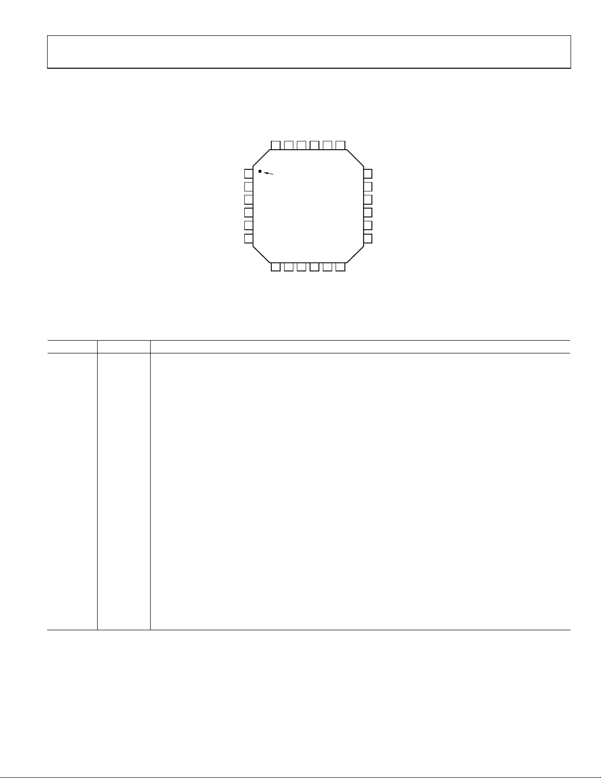
PIN CONFIGURATION AND FUNCTION DESCRIPTIONS
VREF
VRDZ
COMMCOMMVNEG
23 22 21 20 19
24
OUT1
OUT2
18
SCL1
17
BIN1
16
LOG1
15
LOG2
14
BIN2
13
SCL2
04415-0-002
VSUM
INP1
IRF1
IRF2
INP2
VSUM
1
PIN 1
INDICATOR
2
3
4
5
6
7 8 9 10 11 12
VREF
ADL5310
DUAL LOG AMP
TOP VIEW
(Not to Scale)
VPOS
VPOS
VNEG
VNEG
Figure 2. 24-Lead LFCSP Pin Configuration
Table 3. Pin Function Descriptions
Pin No. Mnemonic Function
1, 6 VSUM Guard Pin. Used to shield the INP1 and INP2 input current lines, and for optional adjustment of the input
summing node potentials. Pin 1 and Pin 6 are internally shorted.
2 INP1 Channel 1 Numerator Input. Accepts (sinks) photodiode current I
. Usually connected to photodiode anode
PD1
such that photocurrent flows into INP1.
3 IRF1 Channel 1 Denominator Input. Accepts (sinks) reference current, I
4 IRF2 Channel 2 Denominator Input. Accepts (sinks) reference current, I
5 INP2 Channel 2 Numerator Input. Accepts (sinks) photodiode current I
.
RF1
.
RF2
. Usually connected to photodiode anode
PD2
such that photocurrent flows into INP2.
7, 24 VREF Reference Output Voltage of 2.5 V. Pin 7 and Pin 24 are internally shorted.
8, 9 VPOS Positive Supply, (VP – VN) ≤ 12 V. Both pins must be connected externally.
10, 11, 20 VNEG Optional Negative Supply, VN. These pins are usually grounded. For more details, see the General Structure and
Applications sections. All VNEG pins must be connected externally.
12 OUT2 Buffer Output for Channel 2.
13 SCL2 Buffer Amplifier Inverting Input for Channel 2.
14 BIN2 Buffer Amplifier Noninverting Input for Channel 2.
15 LOG2 Output of the Logarithmic Front End for Channel 2.
16 LOG1 Output of the Logarithmic Front End for Channel 1.
17 BIN1 Buffer Amplifier Noninverting Input for Channel 1.
18 SCL1 Buffer Amplifier Inverting Input for Channel 1.
19 OUT1 Buffer Output for Channel 1.
21, 22 COMM Analog Ground. Pin 21 and Pin 22 are internally shorted.
23 VRDZ Intercept Shift Reference Input. The top of a resistive divider network that offsets VLOG to position the
intercept. Normally connected to VREF; may also be connected to ground when bipolar outputs are to be
provided.
Rev. A | Page 5 of 20

ADL5310
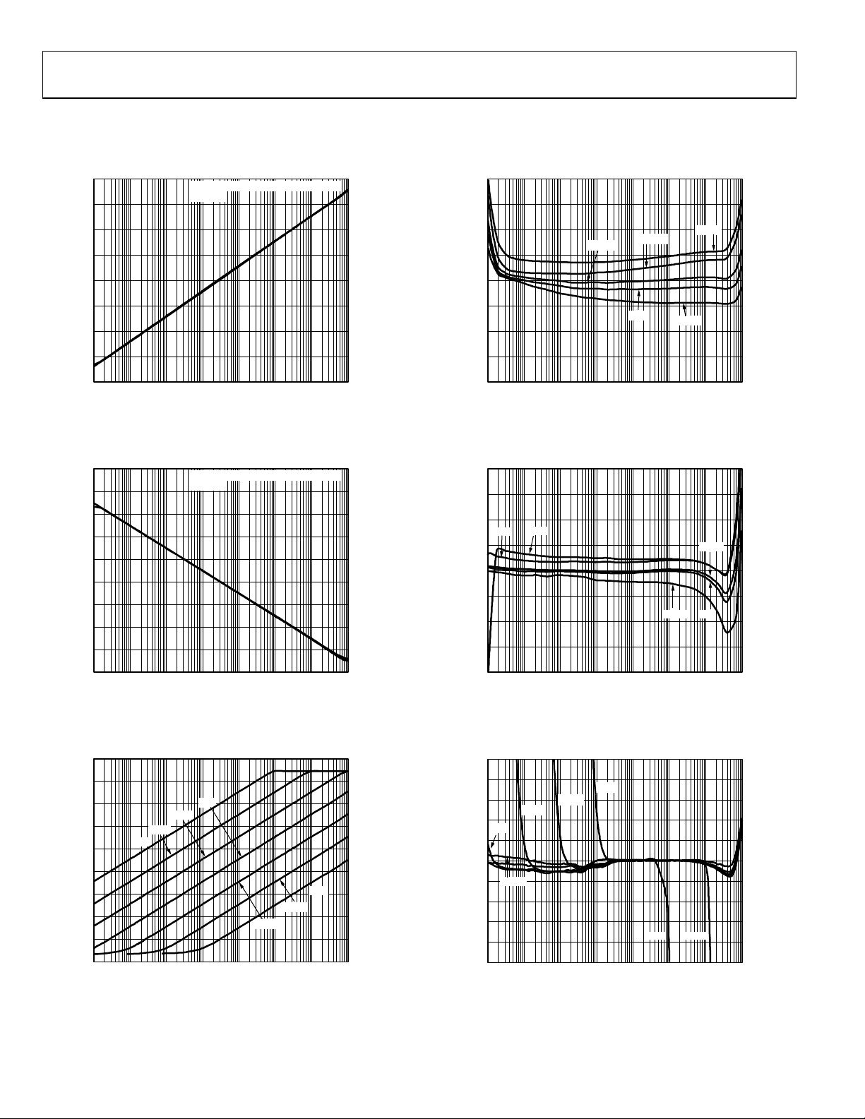
TYPICAL PERFORMANCE CHARACTERISTICS
VP = 5 V, VN = 0 V, R
1.6
1.4
= 665 kΩ, TA = 25°C, unless otherwise noted.
REF
TA = –40°C, 0°C, +25°C, +70°C,
= 0V
V
IN
+85°C
2.0
1.5
1.2
1.0
(V)
0.8
LOG
V
0.6
0.4
0.2
0
1n 10n 100n 1µ 10µ 100µ 1m 10m
I
(A)
INP
vs. I
Figure 3. V
for Multiple Temperatures
LOG
INP
1.8
1.6
1.4
1.2
(V)
1.0
LOG
V
0.8
0.6
0.4
0.2
0
1n 10n 100n 1µ 10µ 100µ 1m 10m
Figure 4. V
LOG
TA = –40°C, 0°C, +25°C, +70°C,
V
= 0V
IN
I
(A)
REF
vs. I
for Multiple Temperatures (I
REF
INP
1.8
1.6
1.4
1.2
(V)
1.0
LOG
V
0.8
0.6
0.4
0.2
0
1n 10n 100n 1µ 10µ 100µ 1m 10m
30nA
3nA
Figure 5. V
3µA
300nA
I
INP
vs. I
for Multiple Values of I
LOG
INP
300µA
30µA
(A)
Decade Steps from 3 nA to 3 mA
+85°C
= 3 µA)
3mA
,
REF
04415-0-003
04415-0-004
04415-0-005
1.0
0.5
0
–0.5
ERROR (dB (10mV/dB))
–1.0
–1.5
–2.0
1n 10n 100n 1µ 10µ 100µ 1m 10m
+25°C
I
INP
Figure 6. Law Conformance Error vs. I
+70°C
0°C
(A)
–40°C
for Multiple Temperatures,
INP
Normalized to 25°C
2.0
1.5
1.0
0.5
0
–0.5
ERROR (dB (10mV/dB))
–1.0
–1.5
–2.0
1n 10n 100n 1µ 10µ 100µ 1m 10m
Figure 7. Law Conformance Error vs. I
1.0
0.8
0.6
0.4
0.2
0
–0.2
–0.4
ERROR (dB (10mV/dB))
–0.6
–0.8
–1.0
1n 10n 100n 1µ 10µ 100µ 1m 10m
Figure 8. Law Conformance Error vs. I
+70°C
3µA
300nA
+85°C
Normalized to 25°C (I
300µA
30µA
I
REF
3mA
I
INP
–40°C
(A)
for Multiple Temperatures,
REF
= 3 µA)
INP
30nA3nA
(A)
for Multiple Values of I
INP
Decade Steps from 3 nA to 3 mA
+85°C
+25°C
0°C
04415-0-006
04415-0-007
04415-0-008
,
REF
Rev. A | Page 6 of 20
 Loading...