Wide Dynamic Range, High Speed,
A
Data Sheet
FEATURES
Dual independent, digitally controlled VGAs
−11.5 dB to +20 dB gain range
0.5 dB ± 0.1 dB step size
150 Ω differential input and output
7.5 dB noise figure at maximum gain
OIP3 > 50 dBm at 200 MHz
−3 dB upper frequency bandwidth of 700 MHz
Multiple control interface options
Parallel 6-bit control interface (with latch)
Serial peripheral interface (SPI) (with fast attack)
Gain up/down mode
Wide input dynamic range
Low power mode option
Power-down control
Single 5 V supply operation
40-lead, 6 mm × 6 mm LFCSP package
APPLICATIONS
Differential ADC drivers
High IF sampling receivers
High output power IF amplification
Instrumentation
Digitally Controlled VGA
ADL5202
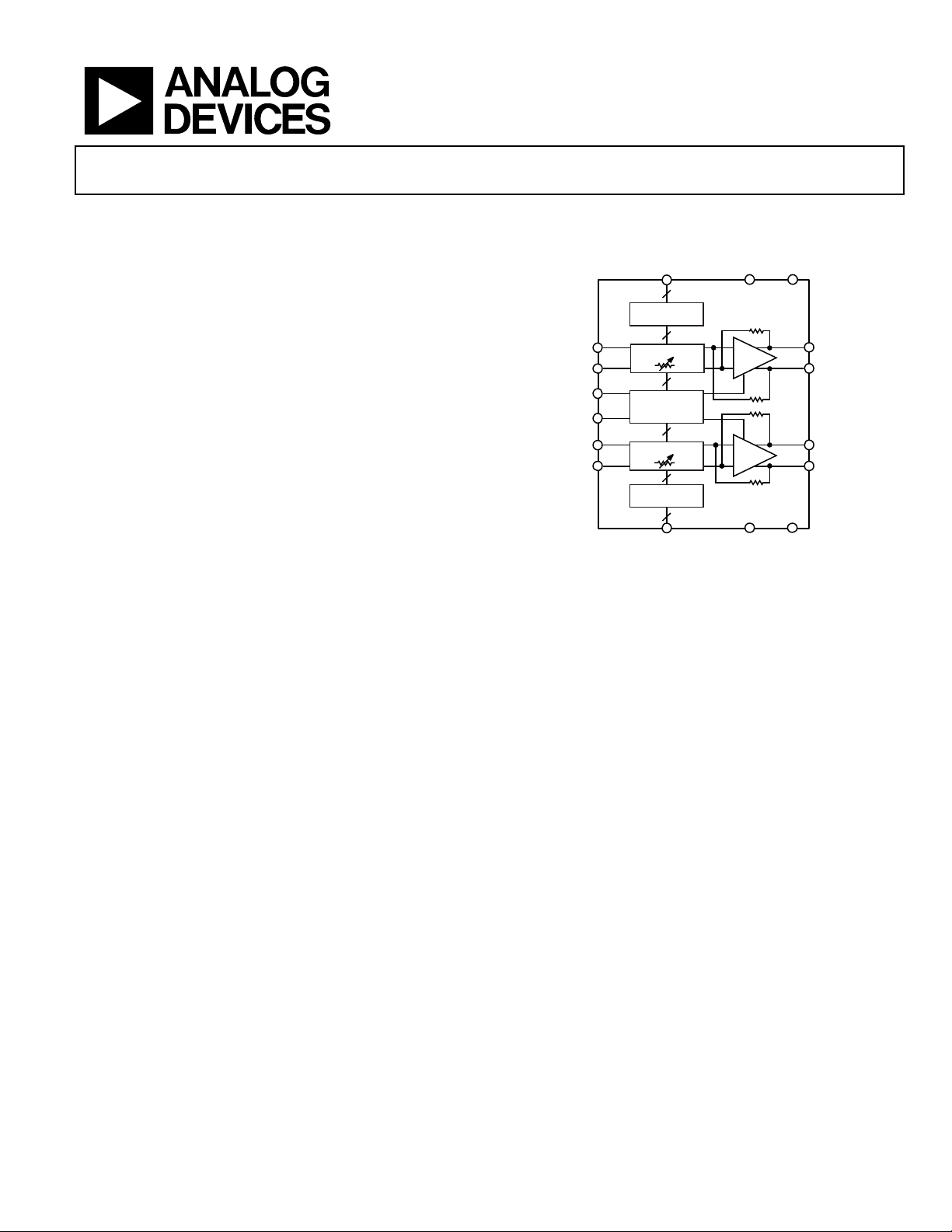
FUNCTIONAL BLOCK DIAGRAM
SIDE
SPI WITH FA,
PARALLEL WITH LATCH,
VINA+
VINA–
MODE0,
MODE1
PM
VINB+
VINB–
UP/DN
LOGIC
0dB TO 31.5d B
150Ω
CONTROL
CIRCUITRY
0dB TO 31.5dB
150Ω
LOGIC
SIDE B
SPI WITH FA,
PARALLEL WITH LATCH,
UP/DN
Figure 1.
PWUPA
+20dB
+20dB
ADL5202
PWUPB
VPOS
150Ω
150Ω
GND
VOUTA+
VOUTA–
VOUTB+
VOUTB–
09387-001
GENERAL DESCRIPTION
The ADL5202 is a digitally controlled, variable gain, wide bandwidth amplifier that provides precise gain control, high output
IP3, and low noise figure. The excellent distortion performance
and high signal bandwidth make the ADL5202 an excellent gain
control device for a variety of receiver applications. The
ADL5202 also incorporates a low power mode option that
lowers the supply current.
For wide input dynamic range applications, the ADL5202
provides a broad 31.5 dB gain range with 0.5 dB resolution. The
gain is adjustable through multiple gain control interface options:
parallel, serial peripheral interface, and up/down.
Incorporating proprietary distortion cancellation techniques,
the ADL5202 achieves a better than 50 dBm output IP3 at
frequencies approaching 200 MHz for most gain settings.
The ADL5202 is powered on by applying the appropriate logic
level to the PWUPx pins. The quiescent current of the ADL5202
is typically 160 mA in low power mode. When configured in high
performance mode for more demanding applications, the quiescent
current is 210 mA. When powered down, the ADL5202 consumes
less than 14 mA and offers excellent input-to-output isolation.
The gain setting is preserved during power-down.
Fabricated on an Analog Devices, Inc., high speed SiGe process,
the ADL5202 provides precise gain adjustment capabilities with
good distortion performance and low phase error. The ADL5202
amplifier comes in a compact, thermally enhanced 40-lead,
6 mm × 6 mm LFCSP package and operates over a temperature
range of −40°C to +85°C.
Rev. 0
Information furnished by Analog Devices is believed to be accurate and reliable. However, no
responsibility is assumed by Anal og Devices for its use, nor for any infringements of patents or ot her
rights of third parties that may result from its use. Specifications subject to change without notice. No
license is granted by implication or otherwise under any patent or patent rights of Analog Devices.
Trademarks and registered trademarks are the property of their respective owners.
One Technology Way, P.O. Box 9106, Norwood, MA 02062-9106, U.S.A.
Tel: 781.329.4700 www.analog.com
Fax: 781.461.3113 ©2011 Analog Devices, Inc. All rights reserved.

ADL5202 Data Sheet
TABLE OF CONTENTS
Features.............................................................................................. 1
Applications....................................................................................... 1
Functional Block Diagram ..............................................................1
General Description......................................................................... 1
Revision History ...............................................................................2
Specifications..................................................................................... 3
Absolute Maximum Ratings............................................................ 5
ESD Caution.................................................................................. 5
Pin Configuration and Functional Descriptions.......................... 6
Typical Performance Characteristics............................................. 8
Characterization and Test Circuits............................................... 15
Theory of Operation ......................................................................16
Digital Interface Overview ........................................................ 16
Parallel Digital Interface............................................................ 16
Serial Peripheral Interface (SPI)............................................... 16
Gain Up/Down Interface........................................................... 16
Truth Table.................................................................................. 17
Logic Timing............................................................................... 17
Circuit Description......................................................................... 18
Basic Structure............................................................................ 18
Applications Information.............................................................. 19
Basic Connections...................................................................... 19
ADC Driving............................................................................... 19
Layout Considerations............................................................... 21
Evaluation Board............................................................................ 22
Evaluation Board Control Software......................................... 22
Evaluation Board Schematics and Artwork............................ 23
Evaluation Board Configuration Options............................... 27
Outline Dimensions....................................................................... 29
Ordering Guide .......................................................................... 29
REVISION HISTORY
10/11—Revision 0: Initial Version
Rev. 0 | Page 2 of 32

Data Sheet ADL5202
SPECIFICATIONS
VS = 5 V, TA = 25°C, RS = RL = 150 Ω at 100 MHz, high performance mode, 2 V p-p differential output, unless otherwise noted.
Table 1.
Parameter Test Conditions/Comments Min Typ Max Unit
DYNAMIC PERFORMANCE
−3 dB Bandwidth V
Slew Rate
Input Return Loss (S11) 100 MHz
Output Return Loss (S22) 100 MHz
INPUT STAGE
Maximum Input Swing (Differential) Gain code = 111111
Differential Input Resistance
Common-Mode Input Voltage
CMRR Gain code = 000000
GAIN
Maximum Voltage Gain Gain code = 000000 20 dB
Minimum Voltage Gain Gain code = 111111 −11.5 dB
Gain Step Size 0.5 dB
Gain Flatness 30 MHz < fC < 200 MHz 0.285 dB
Gain Temperature Sensitivity Gain code = 000000
Gain Step Response For VIN = 0.2 V, gain code = 111111 to 000000
Gain Conformance Error Over 10 dB gain range
Phase Conformance Error Over 10 dB gain range
OUTPUT STAGE
Output Voltage Swing At P1dB, gain code = 000000
Differential Output Resistance Differential
NOISE/HARMONIC PERFORMANCE
46 MHz Gain code = 000000, high performance mode
Second Harmonic V
Third Harmonic V
Output IP3 V
70 MHz Gain code = 000000, high performance mode
Second Harmonic V
Third Harmonic V
Output IP3 V
140 MHz Gain code = 000000, high performance mode
Noise Figure
Second Harmonic V
Third Harmonic V
Output IP3 V
Output 1 dB Compression Point
300 MHz Gain code = 000000, high performance mode
Second Harmonic V
Third Harmonic V
Output IP3 V
< 2 V p-p (5.2 dBm)
OUT
700
5.5
−17.7
−16.5
MHz
V/ns
dB
dB
VINA+, VINB+ and VINA−, VINB− pins
10.8
150
1.5
40
V p-p
Ω
V
dB
0.012
15 ns
±0.03 dB
1.0 Degrees
dB/°C
VOUTx+ and VOUTx− pins
10
150
V p-p
Ω
= 2 V p-p
OUT
= 2 V p-p
OUT
= 2 V p-p composite
OUT
−92
−105
50
dBc
dBc
dBm
= 2 V p-p
OUT
= 2 V p-p
OUT
= 2 V p-p composite
OUT
−96
−105
50
dBc
dBc
dBm
= 2 V p-p
OUT
= 2 V p-p
OUT
= 2 V p-p composite
OUT
7.5
−86
−105
50
19.5
dB
dBc
dBc
dBm
dBm
= 2 V p-p
OUT
= 2 V p-p
OUT
= 2 V p-p composite
OUT
−77
−91
47
dBc
dBc
dBm
Rev. 0 | Page 3 of 32
ADL5202 Data Sheet
Parameter Test Conditions/Comments Min Typ Max Unit
POWER-UP INTERFACE PWUPA, PWUPB pins
Power-Up Threshold Minimum voltage to enable the device 1.4 V
Maximum voltage to enable the device 3.3 V
PWUPx Input Bias Current 1 μA
GAIN CONTROL INTERFACE
VIH Minimum/Maximum voltage for a logic high 1.4 3.3 V
VIL Maximum voltage for a logic low 0.8
Maximum Input Bias Current 1 μA
SPI TIMING LATCHA and LATCHB, SCLK, SDIO, data pins
f
1/t
SCLK
tDH Data hold time 5 ns
tDS Data setup time 5 ns
tPW SCLK high pulse width 5 ns
POWER INTERFACE
Supply Voltage 4.5 5.5 V
Quiescent Current, Both Channels High performance mode
T
Low power mode
T
Power-Down Current, Both Channels PWUPx low
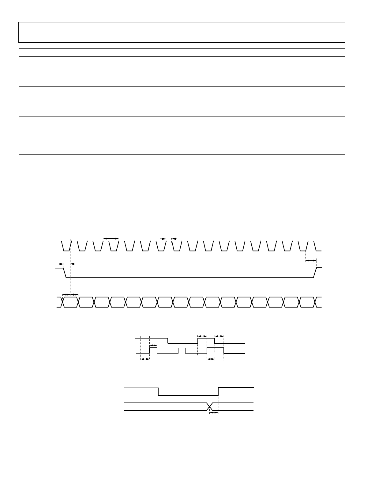
Timing Diagrams
t
SCLK
SCLK
20 MHz
SCLK
= 85°C
A
= 85°C
A
210 mA
250 mA
160 mA
180 mA
14 mA
t
PW
t
DH
09387-002
___ ___
CSA, CSB
SDIO
t
DS
tDSt
DH
DNC DNC DNC DNC DNC DNC DNC R/W FA1 FA0 D5 D4 D3 D2 D1 D0
Figure 2. SPI Interface Read/Write Mode Timing Diagram
t
t
DS
DS
UPDN_DAT
UPDN_CLK
t
PW
DNUP
t
DS
RESET
t
DH
09387-103
Figure 3. Up/Down Mode Timing Diagram
LATCHA,
LATCHB
A5 TO A0
B5 TO B0
t
DH
09387-104
Figure 4. Parallel Mode Timing Diagram
Rev. 0 | Page 4 of 32
Data Sheet ADL5202
ABSOLUTE MAXIMUM RATINGS
Table 2.
Parameter Rating
Supply Voltage, V
PWUPA, PWUPB, A0 to A5, B0 to B5,
MODE0, MODE1, PM, LATCHA, LATCHB
Input Voltage, V
Internal Power Dissipation 1.6 W
θJA (Exposed Paddle Soldered Down) 34.6°C/W
θJC (At Exposed Paddle) 3.6°C/W
Maximum Junction Temperature 140°C
Operating Temperature Range −40°C to +85°C
Storage Temperature Range −65°C to +150°C
Lead Temperature (Soldering, 60 sec) 240°C
5.5
POS
3.6 V
,VIN− +3.6 V to −1.2 V
IN+
Stresses above those listed under Absolute Maximum Ratings
may cause permanent damage to the device. This is a stress
rating only; functional operation of the device at these or any
other conditions above those indicated in the operational
section of this specification is not implied. Exposure to absolute
maximum rating conditions for extended periods may affect
device reliability.
ESD CAUTION
Rev. 0 | Page 5 of 32
ADL5202 Data Sheet
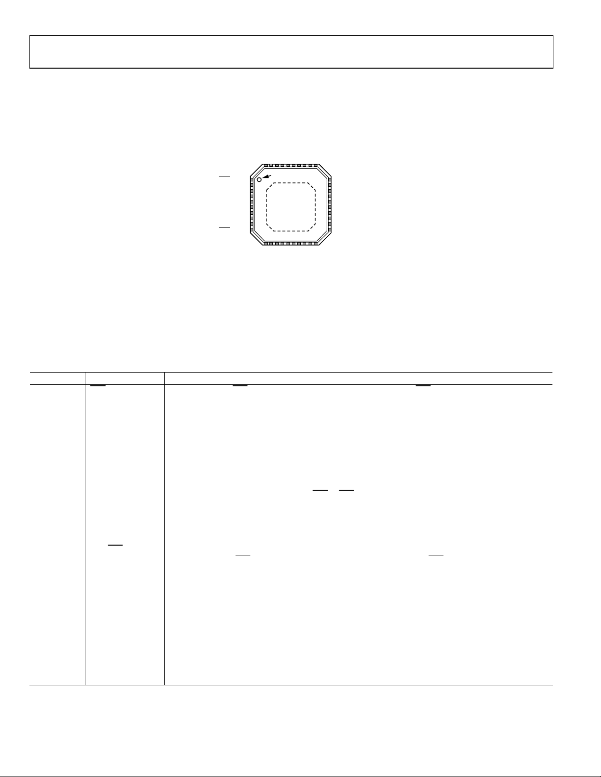
PIN CONFIGURATION AND FUNCTION DESCRIPTIONS
+
A
T
UPA
U
O
GND
PW
VINA+
VINA–
V
VOUTA–
6
31
32
37 LATCHA
3
35
38 UPDN_DAT_A/A0
34
CSA/A3
MODE1
MODE0
PM
GND
SIDO/B5
SCLK/B4
GS1/CSB/B3
39 UPDN_CLK_A/A1
40 FA_A/A2
PIN 1
INDICAT OR
1
2
A4
3
A5
4
5
6
7
8
9
10
ADL5202
TOP VIEW
(Not to Scale)
EXPOSED
PADDLE
33
30
VOUTA–
29
VOUTA+
28
VPOS
27
VPOS
26
VPOS
25
VPOS
VPOS
24
23 VPOS
22
VOUTB+
21
VOUTB–
14
12
13
11
_B/B1
LATCHB
_DAT_B/B0
GS0/FA_B/B2
UPDN_CLK
NOTES
1. NC = NO CONNECT.
2. THE EXPOSED PADDLE (EP) MUST BE CONNECTED TO
A LOW IMPEDANCE GROUND PAD.
UPDN
Figure 5. Pin Configuration
15
VINB–
20
19
16
18
17
UPB
GND
VINB+
PW
VOUTB–
VOUTB+
09387-003
Table 3. Pin Function Descriptions
Pin No. Mnemonic Description
1
/A3 Channel A Select (CSA). When serial mode is enabled, a logic low (0 V ≤ CSA ≤ 0.8 V) selects Channel A.
CSA
Bit 3 for Channel A Parallel Gain Control Interface (A3).
2 A4 Bit 4 for Channel A Parallel Gain Control Interface.
3 A5 Bit 5 (MSB) for Channel A Parallel Gain Control Interface.
4 MODE1 MSB for Mode Control. With the MODE0 pin, selects parallel, SPI, or up/down interface mode.
5 MODE0 LSB for Mode Control. With the MODE1 pin, selects parallel, SPI, or up/down interface mode.
6 PM
Performance Mode. A logic low (0 V ≤ PM ≤ 0.8 V) enables high performance mode. A logic high
(1.4 V ≤ PM ≤ 3.3 V) enables low power mode.
7, 18, 33, EP GND Ground. The exposed paddle (EP) must be connected to a low impedance ground pad.
8 SDIO/B5
Serial Data Input/Output (SDIO). When CSA
or CSB is pulled low, SDIO is used for reading and writing
to the SPI port.
Bit 5 for Channel B Parallel Gain Control Interface (B5).
9 SCLK/B4
Serial Clock Input in SPI Mode (SCLK).
Bit 4 for Channel B Parallel Gain Control Interface (B4).
10
GS1/CSB
/B3 MSB for Gain Step Size Control in Up/Down Mode (GS1).
Channel B Select (CSB
). When serial mode is enabled, a logic low (0 V ≤ CSB≤ 0.8 V ) selects Channel B.
Bit 3 for Channel B Parallel Gain Control Interface (B3).
11 GS0/FA_B/B2
LSB for Gain Step Size Control in Up/Down Mode (GS0).
Fast Attack (FA_B). In serial mode, a logic high (1.4 V ≤ FA_B ≤ 3.3 V) attenuates Channel B according to
the FA setting in the SPI word.
Bit 2 for Channel B Parallel Gain Control Interface (B2).
12 UPDN_CLK_B/B1
Clock Interface for Channel B Up/Down Function (UPDN_CLK_B).
Bit 1 for Channel B Parallel Gain Control Interface (B1).
13 UPDN_DAT_B/B0
Data Pin for Channel B Up/Down Function (UPDN_DAT_B).
Bit 0 for Channel B Parallel Gain Control Interface (B0).
14 LATCHB
Channel B Latch. A logic low (0 V ≤ LATCHB ≤ 0.8 V) allows gain changes on Channel B. A logic high
(1.4 V ≤ LATCHB ≤ 3.3 V) prevents gain changes on Channel B.
Rev. 0 | Page 6 of 32

Data Sheet ADL5202
Pin No. Mnemonic Description
15 VINB− Channel B Negative Input.
16 VINB+ Channel B Positive Input.
17 PWUPB Channel B Power-Up. A logic high (1.4 V ≤ PWUPB ≤ 3.3 V) enables Channel B.
19, 21 VOUTB− Channel B Negative Output.
20, 22 VOUTB+ Channel B Positive Output.
23, 24, 25,
26, 27, 28
29, 31 VOUTA+ Channel A Positive Output.
30, 32 VOUTA− Channel A Negative Output.
34 PWUPA Channel A Power-Up. A logic high (1.4 V ≤ PWUPA ≤ 3.3 V) enables Channel A.
35 VINA+ Channel A Positive Input.
36 VINA− Channel A Negative Input.
37 LATCHA
38 UPDN_DAT_A/A0 Data Pin for Channel A Up/Down Function (UPDN_DAT_A).
39 UPDN_CLK_A/A1
40 FA_A/A2
VPOS Positive Power Supply.
Channel A Latch. A logic low (0 V ≤ LATCHA ≤ 0.8 V) allows gain changes on Channel A. A logic high
(1.4 V ≤ LATCHA ≤ 3.3 V) prevents gain changes on Channel A.
Bit 0 for Channel A Parallel Gain Control Interface (A0).
Clock Interface for Channel A Up/Down Function (UPDN_CLK_A).
Bit 1 for Channel A Parallel Gain Control Interface (A1).
Fast Attack (FA_A). In serial mode, a logic high (1.4 V ≤ FA_A ≤ 3.3 V) attenuates Channel A according to
FA setting in the SPI word.
Bit 2 for Channel A Parallel Gain Control Interface (A2).
Rev. 0 | Page 7 of 32
ADL5202 Data Sheet
TYPICAL PERFORMANCE CHARACTERISTICS
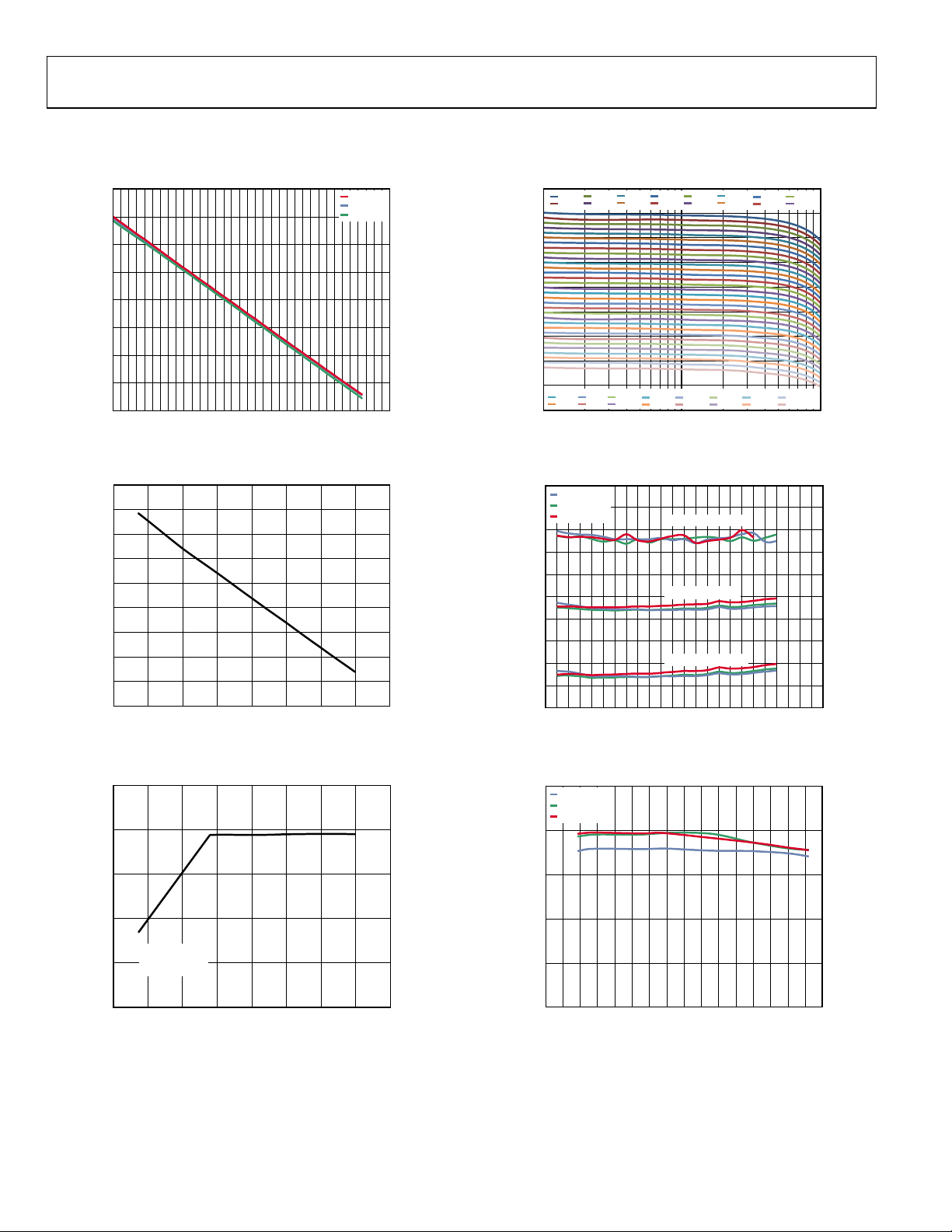
VS = 5 V, TA = 25°C, RS = RL = 150 Ω at 200 MHz, high performance mode, 2 V p-p differential output, unless otherwise noted.
25
20
15
10
5
GAIN (dB)
0
–5
–10
–15
0 10203040506070
GAIN CODE
46MHz
140MHz
300MHz
Figure 6. Gain vs. Gain Code at 46 MHz, 140 MHz, and 300 MHz
09387-004
25
20dB
19dB
20
15
10
5
0
GAIN (dB)
–5
–10
–15
4dB
3dB
–20
10 100 1000
2dB
1dB
18dB
17dB
0dB
–1dB
16dB
14dB
15dB
13dB
–2dB
–4dB
–3dB
–5dB
FREQUENCY (MHz)
12dB
11dB
–6dB
–7dB
10dB
9dB
–8dB
–9dB
8dB
7dB
Figure 9. Gain vs. Frequency Response (Every 1 dB Step)
6dB
5dB
–10dB
–11dB
09387-007
45
40
35
30
25
20
15
NOISE F IGURE (d B)
10
5
0
–15 –10 –5 0 5 10 15 20 25
PROGRAMMED G AIN (dB)
Figure 7. Noise Figure vs. Programmed Gain at 140 MHz
25
20
15
10
OP1dB (dBm)
50
TA = –40°C
= +25°C
T
A
45
= +85°C
T
A
40
35
30
25
20
NOISE F IGURE (dB)
15
10
5
0
0 100 200 300 400 500 600
09387-010
MIN GAIN (–11.5dB)
MID GAIN (5dB)
MAX GAIN (20dB)
FREQUENC Y (MHz)
09387-013
Figure 10. Noise Figure vs. Frequency at Max, Mid, and Min Gain Outputs
25
TA = –40°C
T
= +25°C
A
= +85°C
T
A
20
15
10
OP1dB (dBm)
INPUT
MAX RATINGS
5
BOUNDARY
0
–15 –10 –5 0 5 10 15 20 25
PROGRAMMED GAIN (dB)
Figure 8. OP1dB vs. Programmed Gain at 140 MHz
09387-005
Rev. 0 | Page 8 of 32
5
0
0 50 100 150 200 250 300 350 400
FREQUENC Y (MHz)
Figure 11. OP1dB vs. Frequency at Maximum Gain, Three Temperatures
09387-008
Data Sheet ADL5202
–
–
60
–11.5dB
0dB
10dB
20dB
55
50
45
OIP3 (dBm)
40
35
30
0 50 100 150 200 250 300 350 400
FREQUENCY (MHz)
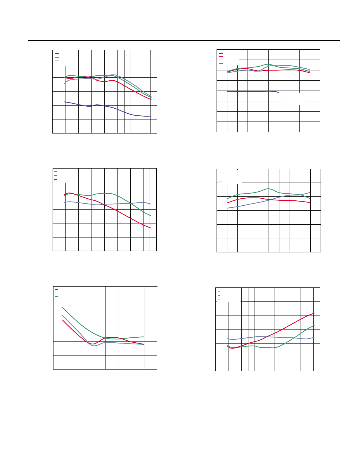
Figure 12. Output Third-Order Intercept vs. Frequency
at Four Gain Codes
60
TA = –40°C
= +25°C
T
A
= +85°C
T
A
55
50
45
OIP3 (dBm)
40
09387-011
60
–11.5dB
0dB
10dB
55
20dB
50
45
40
OIP3 (dBm)
35
30
25
20
–4–3–2–10123456
P
(dBm)
OUT
INPUT
MAX RATINGS
BOUNDARY
Figure 15. Output Third-Order Intercept vs. Power at Four Gain Codes,
Frequency = 140 MHz at 2 V p-p Composite
60
TA = –40°C
T
= +25°C
A
T
= +85°C
A
55
50
45
OIP3 (dBm)
40
09387-014
35
30
0 50 100 150 200 250 300 350 400
FREQUENCY (MHz)
Figure 13. Output Third-Order Intercept vs. Frequency,
Three Temperatures at 2 V p-p Composite
60
46MHz
140MHz
300MHz
–70
–80
–90
IMD3 (dBc)
–100
–110
–120
–15 –10 –5 0 5 10 15 20 25
PROGRAMMED GAIN (dB)
Figure 14. Two-Tone Output IMD3 vs. Programmed Gain,
at 46 MHz, 140 MHz, 300 MHz
35
30
–4 –3 –2 –1 0 1 2 3 4 5 6
09387-016
P
(dBm)
OUT
09387-019
Figure 16. Output Third-Order Intercept vs. Power, Frequency = 140 MHz,
Three Temperatures
60
TA = –40°C
T
= +25°C
A
T
= +85°C
A
–70
–80
–90
IMD3 (dBc)
–100
–110
–120
09387-018
0 50 100 150 200 250 300 350 400
FREQUENCY (MHz)
09387-021
Figure 17. Two-Tone Output IMD3 vs. Frequency,
Three Temperatures
Rev. 0 | Page 9 of 32
ADL5202 Data Sheet
–
–
–
–
–
–
–
–50
–11.5dB
0dB
–60
10dB
20dB
–70
–80
–90
–100
–110
–120
–130
HARMONIC DIS TORTI ON HD2 (dBc)
–140
–150
0 50 100 150 200 250 300 350
FREQUENC Y (MHz)
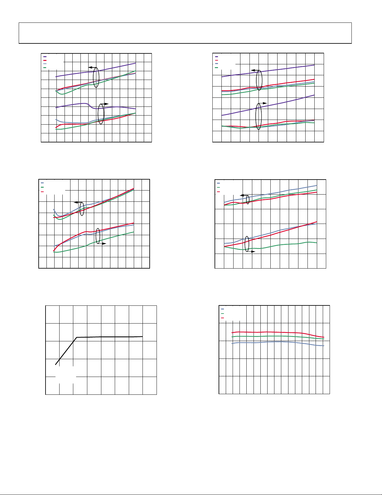
Figure 18. Harmonic Distortion vs. Frequency at Four Gain Codes
60
TA = –40°C
T
= +25°C
A
–70
T
= +85°C
A
–80
–90
–100
–110
–120
HARMONIC DISTORTION HD2 (dBc)
–130
–30
–40
–50
–60
–70
–80
–90
–100
–110
–120
40
–50
–60
–70
–80
–90
–100
–110
20
HARMONIC DIS TORTI ON HD3 (dBc)
09387-023
60
–11.5dB
0dB
10dB
–70
20dB
–80
–90
–100
–110
–120
HARMONIC DISTORTION HD2 (dBc)
–130
–140
–6 –5 –4 –3 –2 –1 0 1 2 3 4 5 6
P
(dBm)
OUT
40
–50
–60
–70
–80
–90
–100
–110
–120
HARMONIC DISTO RTION HD3 (dBc)
09387-026
Figure 21. Harmonic Distortion vs. Power at Four Gains,
Frequency = 140 MHz
80
TA = –40°C
= +25°C
T
A
= +85°C
T
A
–90
–100
–110
–120
HARMONIC DISTORTION HD3 (dBc)
–130
HARMONIC DISTORTI ON HD2 (dBc)
60
–70
–80
–90
–100
–110
HARMONIC DISTORTI ON HD3 (dBc)
–140
0 50 100 150 200 250 300 350
FREQUENCY (MHz)
–120
Figure 19. Harmonic Distortion vs. Frequency, Three Temperatures
25
20
15
10
OP1dB (dBm)
INPUT
MAX
RATINGS
5
BOUNDARY
0
–15 –10 –5 0 5 10 15 20 25
PROGRAMMED GAIN (dB)
Figure 20. OP1dB vs. Programmed Gain at 140 MHz, Low Power Mode
–140
–6–5–4–3–2–10123456
P
09387-028
OUT
(dBm)
–120
09387-031
Figure 22. Harmonic Distortion vs. Power, Frequency = 140 MHz,
Three Temperatures
25
TA = –40°C
T
= +25°C
A
= +85°C
T
A
20
15
10
OP1dB (dBm)
5
0
0 50 100 150 200 250 300 350 400
09387-006
FREQUENC Y (MHz)
09387-009
Figure 23. OP1dB vs. Frequency at Maximum Gain, Three Temperatures,
Low Power Mode
Rev. 0 | Page 10 of 32
 Loading...