

Ten Degrees of Freedom Inertial Sensor
ADIS16407
Rev. C
rights of third parties that may result from its use. Specifications subject to change without notice. No
Trademarks and registered trademarks are the prop erty of their respective owner s.
Fax: 781.461.3113 ©2011 Analog Devices, Inc. All rights reserved.
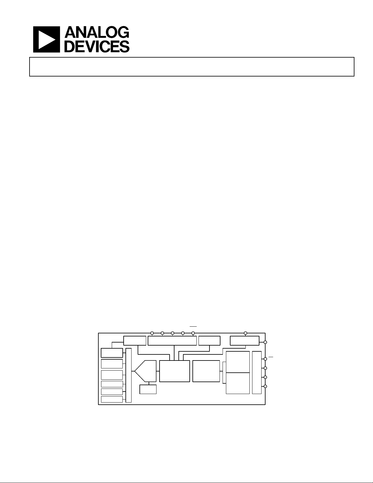
CONTROLLLER
CLOCK
TRIAXIAL
GYRO
TRIAXIAL
ACCEL
POWER
MANAGEMENT
CS
SCLK
DIN
DOUT
GND
VDD
TEMP
VDD
DIO1
DIO2
DIO3
DIO4
RST
SPI
TRIAXIAL
MAGN
PRESSURE
SELF TEST I/O ALARMS
OUTPUT
DATA
REGISTERS
USER
CONTROL
REGISTERS
CALIBRATION
AND
FILTERS
ADIS16407
09797-001
Data Sheet
FEATURES
Triaxial digital gyroscope with digital range scaling
±75°/sec, ±150°/sec, ±300°/sec settings
Axis-to-axis alignment, <0.05°
Triaxial digital accelerometer, ±18 g minimum
Triaxial digital magnetometer, ±2.5 gauss minimum
Digital barometer, 10 mbar to 1200 mbar
Calibrated pressure range: 300 mbar to 1100 mbar
Autonomous operation and data collection
No external configuration commands required
210 ms start-up time, 4 ms sleep mode recovery time
Factory calibrated sensitivity, bias, and axial alignment
Calibration temperature range: −40°C to +85°C
SPI-compatible serial interface
Embedded temperature sensor
Programmable operation and control
Automatic and manual bias correction controls
Bartlett window FIR length, number of taps
Digital I/O: data ready, alarm indicator, general-purpose
Alarms for condition monitoring
Sleep mode for power management
DAC output voltage
Enable external sample clock input up to 1.1 kHz
Single command self test
Single-supply operation: 4.75 V to 5.25 V
2000 g shock survivability
Operating temperature range: −40°C to +105°C
GENERAL DESCRIPTION
The ADIS16407 iSensor® device is a complete inertial system
that includes a triaxial gyroscope, a triaxial accelerometer, a
triaxial magnetometer, and pressure sensors. Each sensor in
the ADIS16407 combines industry-leading iMEMS® technology
with signal conditioning that optimizes dynamic performance.
The factory calibration characterizes each sensor for sensitivity,
bias, alignment, and linear acceleration (gyro bias). As a result,
each sensor has its own dynamic compensation formulas that
provide accurate sensor measurements.
The ADIS16407 provides a simple, cost-effective method for
integrating accurate, multiaxis inertial sensing into industrial
systems, especially when compared with the complexity and
investment associated with discrete designs. All necessary motion
testing and calibration are part of the production process at the
factory, greatly reducing system integration time. Tight orthogonal
alignment simplifies inertial frame alignment in navigation systems.
The SPI and register structure provide a simple interface for
data collection and configuration control.
The ADIS16407 has a compatible pinout for systems that currently
use ADIS1635x, ADIS1636x, and ADIS1640x IMU products.
The ADIS16407 is packaged in a module that is approximately
23 mm × 23 mm × 23 mm and has a standard connector interface.
APPLICATIONS
Platform stabilization and control
Navigation
Robotics
FUNCTIONAL BLOCK DIAGRAM
Information furnished by Analog Devices is believed to be accurate and reliable. However, no
responsibility is assumed by Analog Devices for its use, nor for any infringements of patents or other
license is granted by implication or otherwise under any patent or patent rights of Analog Devices.
Figure 1.
One Technology Way, P.O. Box 9106, Norwood, MA 02062-9106, U.S.A.
Tel: 781.329.4700 www.analog.com

ADIS16407 Data Sheet
TABLE OF CONTENTS
Features .............................................................................................. 1
Applications ....................................................................................... 1
General Description ......................................................................... 1
Functional Block Diagram .............................................................. 1
Revision History ............................................................................... 2
Specifications ..................................................................................... 3
Timing Specifications .................................................................. 6
Absolute Maximum Ratings ............................................................ 7
ESD Caution .................................................................................. 7
Pin Configuration and Function Descriptions ............................. 8
Typical Performance Characteristics ............................................. 9
Basic Operation ............................................................................... 10
Reading Sensor Data .................................................................. 10
Output Data Registers ................................................................ 11
Input ADC Channel ................................................................... 13
Device Configuration ................................................................ 13
User Registers .................................................................................. 14
System Functions ............................................................................ 15
Global Commands ..................................................................... 15
Power Management .................................................................... 15
Product Identification ................................................................ 15
Memory Management ............................................................... 15
Self Test Function ....................................................................... 16
Status/Error Flags ....................................................................... 16
Input/Output Configuration ......................................................... 17
Data Ready Indicator ................................................................. 17
General-Purpose Input/Output................................................ 17
Auxiliary DAC ............................................................................ 17
Digital Processing Configuration ................................................. 18
Sample Rate ................................................................................. 18
Input Clock Configuration ....................................................... 18
Digital Filtering........................................................................... 18
Dynamic Range .......................................................................... 18
Calibration ....................................................................................... 19
Gyroscopes .................................................................................. 19
Accelerometers ........................................................................... 20
Magnetometer Calibration ........................................................ 20
Flash Updates .............................................................................. 21
Restoring Factory Calibration .................................................. 21
Alarms .............................................................................................. 22
Static Alarm Use ......................................................................... 22
Dynamic Alarm Use .................................................................. 22
Alarm Reporting ........................................................................ 22
Applications Information .............................................................. 23
Installation/Handling................................................................. 23
Gyroscope Bias Optimization ................................................... 23
Interface Printed Circuit Board (PCB) .................................... 23
Outline Dimensions ....................................................................... 24
Ordering Guide .......................................................................... 24
REVISION HISTORY
10/11—Rev. B to Rev. C
Change to Burst Read Function Section and Figure 12 ............ 10
Changed .25 mg to 3.333 mg ........................................ Throughout
Changes to System Functions Section ......................................... 15
Change to Product Identification Section ................................... 15
Change to Table 36 ......................................................................... 15
Changes to Digital Filtering Section, Table 47, Caption for
Figure 18, and Figure 19 ................................................................ 18
Change to Table 67 ......................................................................... 22
7/11—Rev. A to Rev. B
Change to Table 1, Barometer, Sensitivity Parameter .................. 4
Rev. C | Page 2 of 24
Added Barometer Section; Changes to Table 40 ........................ 16
Changes to Table 55, Table 56, Table 57 ...................................... 20
Changes to Table 58, Table 59, Table 60 ...................................... 21
6/11—Rev. 0 to Rev. A
Changes to Device Configuration Section and Figure 16 ......... 13
Changes to Figure 19 ...................................................................... 18
Changes to Figure 25 Caption ...................................................... 24
Changes to Ordering Guide .......................................................... 24
4/11—Revision 0: Initial Version

Data Sheet ADIS16407
Misalignment
Axis to axis
±0.05
Degrees
3 dB Bandwidth
330 Hz
Dynamic Range
±18
g
Output Noise
No filtering
9
mg rms
Nonlinearity
Best fit straight line
0.5 % of FS
SPECIFICATIONS
TA = 25°C, VDD = 5 V, angular rate = 0°/sec, dynamic range = ±300°/sec ± 1 g, unless otherwise noted.
Table 1.
Parameter Test Conditions/Comments Min Typ Max Unit
GYROSCOPES
Dynamic Range ±300 ±350 °/sec
Initial Sensitivity Dynamic range = ±300°/sec 0.0495 0.05 0.0505 °/sec/LSB
Dynamic range = ±150°/sec 0.025 °/sec/LSB
Dynamic range = ±75°/sec 0.0125 °/sec/LSB
Sensitivity Temperature Coefficient −40°C ≤ TA ≤ +85°C ±40 ppm/°C
Axis to frame (package) ±0.5 Degrees
Nonlinearity Best fit straight line ±0.1 % of FS
Initial Bias Error ±1 σ ±3 °/sec
In-Run Bias Stability 1 σ, SMPL_PRD = 0x0001 0.007 °/sec
Angular Random Walk 1 σ, SMPL_PRD = 0x0001 1.9 °/√hr
Bias Temperature Coefficient −40°C ≤ TA ≤ +85°C ±0.01 °/sec/°C
Linear Acceleration Effect on Bias Any axis, 1 σ (MSC_CTRL[7] = 1) 0.05 °/sec/g
Bias Voltage Sensitivity VDD = 4.75 V to 5.25 V ±0.3 °/sec/V
Output Noise ±300°/sec range, no filtering 0.8 °/sec rms
Rate Noise Density f = 25 Hz, ±300°/sec range, no filtering 0.044 °/sec/√Hz rms
Sensor Resonant Frequency 14.5 kHz
ACCELEROMETERS Each axis
Initial Sensitivity 3.285 3.33 3.38 mg/LSB
Sensitivity Temperature Coefficient −40°C ≤ TA ≤ +85°C ±50 ppm/°C
Misalignment Axis to axis 0.2 Degrees
Axis to frame (package) ±0.5 Degrees
Nonlinearity Best fit straight line 0.1 % of FS
Initial Bias Error ±1 σ ±50 mg
In-Run Bias Stability 1 σ, SMPL_PRD = 0x0001 0.2 mg
Velocity Random Walk 1 σ, SMPL_PRD = 0x0001 0.2 m/sec/√hr
Bias Temperature Coefficient −40°C ≤ TA ≤ +85°C
Bias Voltage Sensitivity VDD = 4.75 V to 5.25 V 2.5 mg/V
Noise Density No filtering 0.5 mg/√Hz rms
3 dB Bandwidth 330 Hz
Sensor Resonant Frequency 5.5 kHz
MAGNETOMETER
Dynamic Range ±2.5 ±3.5 gauss
Initial Sensitivity 25°C 0.49 0.5 0.51 mgauss/LSB
Sensitivity Temperature Coefficient 25°C, 1 σ 600 ppm/°C
Misalignment Axis to axis 0.25 Degrees
Axis to frame (package) 0.5 Degrees
±0.3 mg/°C
Initial Bias Error 25°C, 0 gauss stimulus ±4 mgauss
Bias Temperature Coefficient −40°C ≤ TA ≤ +85°C 0.5 mgauss/°C
Output Noise
Noise Density
Bandwidth −3 dB 1540 Hz
25°C, no filtering, rms
25°C, no filtering, rms
Rev. C | Page 3 of 24
1.15 mgauss
0.06 mgauss/√Hz

ADIS16407 Data Sheet
Sensitivity
0.3125
µbar/LSB
CS Wake-Up Pulse Width
20
μs
Sleep Mode Recovery Time
7 ms
Parameter Test Conditions/Comments Min Typ Max Unit
BAROMETER
Pressure Range
Operating 300 1100 mbar
Extended1 10 1200 mbar
Total Error 25°C, 300 mbar to 1100 mbar 1.5 mbar
Relative Error2 −40°C to +85°C, 300 mbar to 1100 mbar 2.5 mbar
Linearity3 25°C, 300 mbar to 1100 mbar 0.1 % of FS
−40°C to +85°C, 300 mbar to 1100 mbar 0.15 % of FS
Noise 0.027 mbar rms
TEMPERATURE SENSOR
Scale Factor 25°C, output = 0x0000 0.14 °C/LSB
ADC INPUT
Resolution 12 Bits
Integral Nonlinearity ±2 LSB
Differential Nonlinearity ±1 LSB
Offset Error ±4 LSB
Gain Error ±2 LSB
Input Range 0 3.3 V
Input Capacitance During acquisition 20 pF
DAC OUTPUT 5 kΩ/100 pF to GND
Resolution 12 Bits
Relative Accuracy 101 LSB ≤ input code ≤ 4095 LSB ±4 LSB
Differential Nonlinearity ±1 LSB
Offset Error ±5 mV
Gain Error ±0.5 %
Output Range 0 3.3 V
Output Impedance 2 Ω
Output Settling Time 10 µs
LOGIC INPUTS4
Input High Voltage, VIH 2.0 V
Input Low Voltage, VIL 0.8 V
CS signal to wake up from sleep mode
0.55 V
Logic 1 Input Current, IIH VIH = 3.3 V ±0.2 ±10 µA
Logic 0 Input Current, IIL VIL = 0 V
All Pins Except RST
RST Pin
Input Capacitance, CIN 10 pF
DIGITAL OUTPUTS4
Output High Voltage, VOH I
Output Low Voltage, VOL I
FLASH MEMORY Endurance5 10,000 Cycles
Data Retention6 TJ = 85°C 20 Years
FUNCTIONAL TIMES7 Time until new data is available
Power-On Start-Up Time 220 ms
Reset Recovery Time 105 ms
Flash Memory Update Time 75 ms
Flash Memory Test Time 30 ms
Automatic Self Test Time SMPL_PRD = 0x0001 52 ms
40 60 µA
1 mA
= 1.6 mA 2.4 V
SOURCE
= 1.6 mA 0.4 V
SINK
Rev. C | Page 4 of 24

Data Sheet ADIS16407
Sync Input Clock9
0.8 1.1
kHz
Sleep mode
1.4 mA
Parameter Test Conditions/Comments Min Typ Max Unit
CONVERSION RATE SPS
xGYRO_OUT, xACCL_OUT, xMAGN_OUT SMPL_PRD = 0x0001 819.2 SPS
BAR_OUT, BARO_OUTL8 SMPL_PRD = 0x0001 51.2 SPS
Clock Accuracy ±3 %
POWER SUPPLY Operating voltage range, VDD 4.75 5.0 5.25 V
Power Supply Current 70 mA
1
The extended pressure range is guaranteed by design.
2
The relative error assumes that the initial error, at +25°C, is corrected in the end application.
3
Linearity errors assume a full scale (FS) of 1000 mbar.
4
The digital I/O signals are driven by an internal 3.3 V supply, and the inputs are 5 V tolerant.
5
Endurance is qualified as per JEDEC Standard 22, Method A117, and measured at −40°C, +25°C, +85°C, and +125°C.
6
The data retention lifetime equivalent is at a junction temperature (TJ) of 85°C as per JEDEC Standard 22, Method A117. Data retention lifetime decreases with junction
temperature.
7
These times do not include thermal settling and internal filter response times (330 Hz bandwidth), which may affect overall accuracy.
8
The BARO_OUT and BARO_OUTL registers sample at a rate that is 1/16th that of the other output registers.
9
The sync input clock functions below the specified minimum value, but at reduced performance levels.
Rev. C | Page 5 of 24
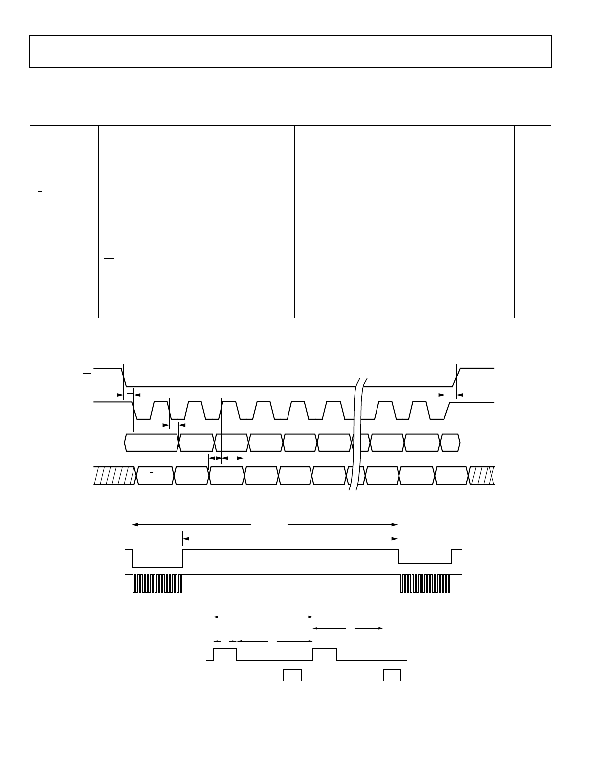
ADIS16407 Data Sheet
tCS
Chip select to SCLK edge
48.8
48.8
ns
t
5 5 ns
CS
SCLK
DOUT
DIN
1 2 3 4 5 6 15 16
R/W A5A6 A4 A3 A2
D2
MSB
DB14
D1 LSB
DB13 DB12 DB10DB11 DB2 LSBDB1
t
CS
t
SFS
t
DAV
t
DHD
t
DSU
09797-002
CS
SCLK
t
READRATE
t
STALL
09797-003
t
3
t
X
t
2
t
1
SYNC
CLOCK (DIO 4)
DATA
READY
07570-004
TIMING SPECIFICATIONS
TA = 25°C, VDD = 5 V, unless otherwise noted.
Table 2.
Normal Mode Burst Read
Parameter Description Min1 Typ Max Min1 Typ Max Unit
f
Serial clock 0.01 2.0 0.01 1.0 MHz
SCLK
t
Stall period between data 9 1/f
STA LL
t
Read rate 40 µs
READRATE
t
DOUT valid after SCLK edge 100 100 ns
DAV
t
DIN setup time before SCLK rising edge 24.4 24.4 ns
DSU
t
DIN hold time after SCLK rising edge 48.8 48.8 ns
DHD
t
, t
SCLKR
SCLK rise/fall times, not shown in Timing Diagrams 5 12.5 5 12.5 ns
SCLKF
tDR, tDF DOUT rise/fall times, not shown in Timing Diagrams 5 12.5 5 12.5 ns
SFS
t
1
CS high after SCLK edge
Input sync positive pulse width 5 5 µs
tx Input sync low time 100 100 µs
t
2
t
3
1
Guaranteed by design and characterization, but not tested in production.
Input sync to data ready output 600 600 µs
Input sync period 910 910 µs
Timing Diagrams
µs
SCLK
Figure 2. SPI Timing and Sequence
Figure 3. Stall Time and Data Rate
Figure 4. Input Clock Timing Diagram
Rev. C | Page 6 of 24
Data Sheet ADIS16407
Any Axis, Unpowered
2000 g
Temperature
ABSOLUTE MAXIMUM RATINGS
Table 3.
Parameter Rating
Acceleration
Any Axis, Powered 2000 g
VDD to GND −0.3 V to +6.0 V
Digital Input Voltage to GND −0.3 V to +5.3 V
Digital Output Voltage to GND −0.3 V to +3.6 V
Analog Input to GND −0.3 V to +3.6 V
Operating Range −40°C to +105°C
Storage Range −65°C to +125°C
Pressure 6 bar
1
Extended exposure to temperatures outside the specified temperature
range of −40°C to +105°C can adversely affect the accuracy of the factory
calibration. For best accuracy, store the parts within the specified operating
range of −40°C to +105°C.
2
Although the device is capable of withstanding short-term exposure to
150°C, long-term exposure threatens internal mechanical integrity.
1, 2
Stresses above those listed under Absolute Maximum Ratings
may cause permanent damage to the device. This is a stress
rating only; functional operation of the device at these or any
other conditions above those indicated in the operational
section of this specification is not implied. Exposure to absolute
maximum rating conditions for extended periods may affect
device reliability.
Table 4. Package Characteristics
Package Type θJA θJC Device Weight
24-Lead Module
39.8°C/W 14.2°C/W 16 grams
(ML-24-2)
ESD CAUTION
Rev. C | Page 7 of 24
ADIS16407 Data Sheet
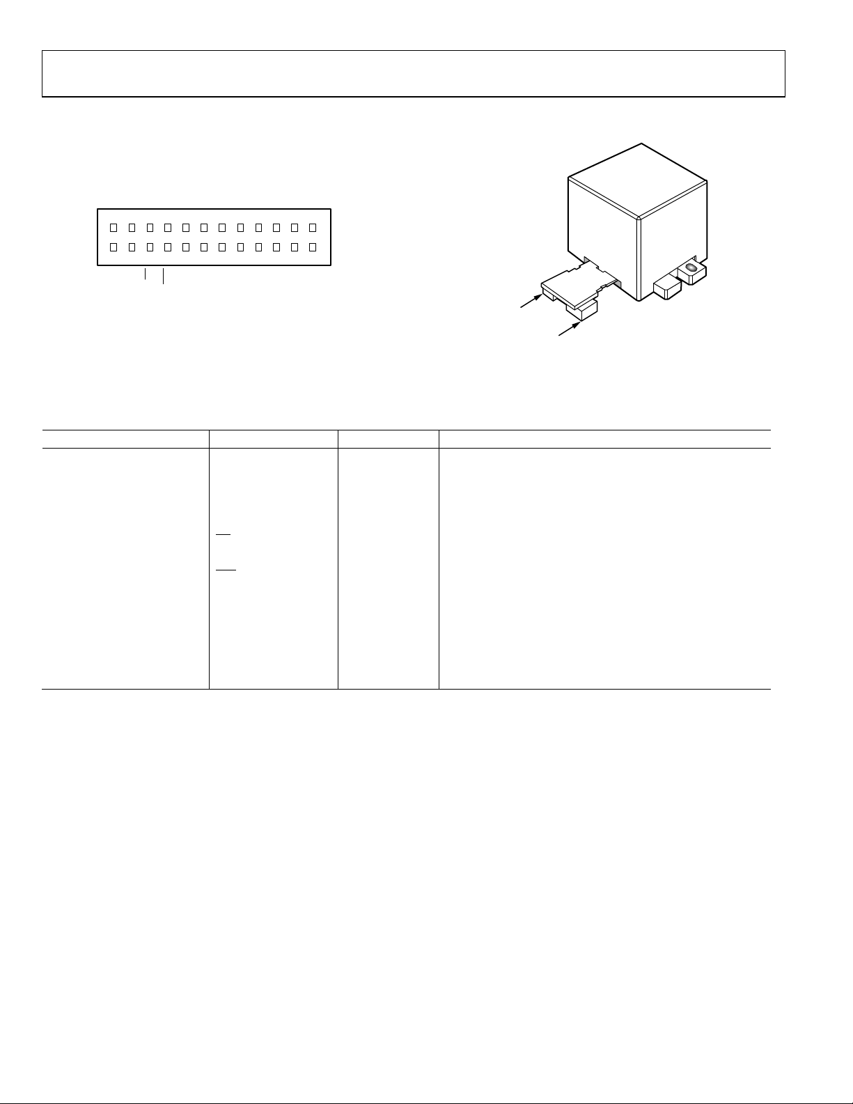
NOTES
1. THIS VIEW REPRESENTS THE TOP VIEW OF THE MATING CONNECTOR.
2. WHE N CONNECTED, THE PINS ARE NOT VISIBLE.
3. MAT ING CONNECT OR: SAMTEC CLM-112-02 OR EQUIVALENT .
4. DNC = DO NOT CONNECT.
1
DIO3
SCLK
DIN
DIO1
DIO2
VDD
GND
GND
DNC
DNC
AUX_ADC
DNC
DIO4/CLKIN
DOUT
CS
RST
VDD
VDD
GND
DNC
DNC
AUX_DAC
DNC
DNC
23456789101112131415161718192021222324
ADIS16407
TOP VIEW
(Not to S cale)
09797-005
PIN 1
PIN 23
09797-006
1
DIO3
I/O
Configurable Digital Input/Output.
PIN CONFIGURATION AND FUNCTION DESCRIPTIONS
Figure 5. Pin Configuration
Figure 6. Axial Orientation
Table 5. Pin Function Descriptions
Pin No. Mnemonic Type1 Description
2 DIO4/CLKIN I/O Configurable Digital Input/Output or Sync Clock Input.
3 SCLK I SPI Serial Clock.
4 DOUT O SPI Data Output. Clocks the output on the SCLK falling edge.
5 DIN I SPI Data Input. Clocks the input on the SCLK rising edge.
6
CS
I SPI Chip Select.
7 DIO1 I/O Configurable Digital Input/Output.
8
RST
I Reset.
9 DIO2 I/O Configurable Digital Input/Output.
10, 11, 12 VDD S Power Supply.
13, 14, 15 GND S Power Ground.
16, 17, 18, 19, 22, 23, 24 DNC N/A Do Not Connect. Do not connect to these pins.
20 AUX_DAC O Auxiliary, 12-Bit DAC Output.
21 AUX_ADC I Auxiliary, 12-Bit ADC Input.
1
S is supply, O is output, I is input, N/A is not applicable.
Rev. C | Page 8 of 24

Data Sheet ADIS16407
0.001
0.01
0.1
0.1 1 10 100 1k 10k
Tau (sec)
ROOT ALLAN VARIANCE (°/sec)
–1σ
MEAN
+1σ
09797-007
0.0001
0.001
0.01
0.1 1 10 100 1k 10k
Tau (sec)
ROOT ALLAN V
ARIANCE (g)
–1σ
MEAN
+1σ
09797-008
TYPICAL PERFORMANCE CHARACTERISTICS
Figure 7. Gyroscope Root Allan Variance
Figure 8. Accelerometer Root Allan Variance
Rev. C | Page 9 of 24

ADIS16407 Data Sheet
SYSTEM
PROCESSOR
SPI MASTER
ADIS16407
SCLK
CS
DIN
DOUT
SCLK
SS
MOSI
MISO
5V
IRQ
DIO1
VDD
I/O LINES ARE COMPATIBLE WITH
3.3V OR 5V LOGIC LEVELS
10
6
3
5
4
7
11
12
13
14
15
09797-009
XGYRO_OUT
DIN
DOUT
YGYRO_OUT
ZGYRO_OUT
0x0400 0x0600
0x0800
09797-010
DOUT = 1111 1001 1101 1010 = 0xF9DA = –1574 LSBs => –19.675°/ sec
DIN = 0000 0100 0000 0000 = 0x0400
SCLK
CS
DIN
DOUT
09797-011
0x4200
DON’T CARE
1 2 3 15
CS
SCLK
DIN
DOUT
XGYRO_OUTSUPPLY_OUT
AUX_ADC
09797-012
R/W
R/W
A6 A5 A4 A3 A2 A1 A0 DC7 DC6 DC5 DC4 DC3 DC2 DC1 DC0
D0D1D2D3D4D5D6D7D8D9D10D11D12D13D14D15
CS
SCLK
DIN
DOUT
A6 A5
D13D14D15
NOTES
1. THE DOUT BIT PATTERN REFLECTS THE ENTIRE CONTENTS OF THE REGISTER IDENTIFIED BY [A6:A0]
IN THE PREVIOUS 16-BIT DIN SEQUENCE W HE N R/W = 0.
2. IF R/W = 1 DURING THE P RE V IOUS SEQUE NCE , DOUT IS NOT DEFINE D.
09797-013
BASIC OPERATION
The ADIS16407 is an autonomous system that requires no user
initialization. When it has a valid power supply, it initializes itself
and starts sampling, processing, and loading sensor data into
the output registers at a sample rate of 819.2 SPS. DIO1 pulses
high after each sample cycle concludes. The SPI interface enables
simple integration with many embedded processor platforms,
as shown in Figure 9 (electrical connection) and Ta ble 6 (pin
functions).
READING SENSOR DATA
The ADIS16407 provides two different options for acquiring
sensor data: single register and burst register. A single register
read requires two 16-bit SPI cycles. The first cycle requests the
contents of a register using the bit assignments in Figure 13.
Bit DC7 to Bit DC0 are don’t care for a read, and then the output
register contents follow on DOUT during the second sequence.
Figure 10 includes three single register reads in succession. In
this example, the process starts with DIN = 0x0400 to request
the contents of XGYRO_OUT, then follows with 0x0600 to
request YGYRO_OUT and 0x0800 to request ZGYRO_OUT.
Full duplex operation enables processors to use the same 16-bit
SPI cycle to read data from DOUT while requesting the next set
of data on DIN. Figure 11 provides an example of the four SPI
signals when reading XGYRO_OUT in a repeating pattern.
Figure 9. Electrical Connection Diagram
Table 6. Generic Master Processor Pin Names and Functions
Pin Name Function
SS
Slave select
SCLK Serial clock
MOSI Master output, slave input
MISO Master input, slave output
IRQ Interrupt request
The ADIS16407 SPI interface supports full duplex serial communication (simultaneous transmit and receive) and uses the bit
sequence shown in Figure 13. Tabl e 7 provides a list of the most
common settings that require attention to initialize the serial
port of a processor for the ADIS16407 SPI interface.
Table 7. Generic Master Processor SPI Settings
Processor Setting Description
Master The ADIS16407 operates as a slave
SCLK Rate ≤ 2 MHz1 Maximum serial clock rate
SPI Mode 3 CPOL = 1 (polarity), CPHA = 1 (phase)
MSB-First Mode Bit sequence
16-Bit Mode Shift register/data length
1
For burst read, SCLK rate ≤ 1 MHz.
Figure 10. SPI Read Example
Figure 11. Example SPI Read, Second 16-Bit Sequence
Burst Read Function
The burst read function enables the user to read all output registers
using one command on the DIN line and shortens the stall time
between each 16-bit segment to one SCLK cycle (see Tabl e 2).
Figure 12 provides the burst read sequence of data on each SPI
signal. The sequence starts with writing 0x4200 to DIN, followed
by each output register clocking out on DOUT, in the order in
which they appear in Ta b le 8.
Figure 12. Burst Read Sequence
Figure 13. SPI Communication Bit Sequence
Rev. C | Page 10 of 24

Data Sheet ADIS16407
ZGYRO_OUT
0x08
Gyroscope, z-axis
Y-AXIS
a
Y
g
Y
g
X
X-AXIS
a
X
Z-AXIS
a
Z
g
Z
m
X
m
Y
m
Z
09797-014
[13:0]
[14]
Error/alarm, 1 = active, see DIAG_STAT for error flags
+300°/sec
+6000
0x1770
xx01 0111 0111 0000
[14]
Error/alarm, 1 = active, see DIAG_STAT for error flags
[15]
New data indicator (ND), 1 = new data in register
[13:0]
Z-axis acceleration data, twos complement format,
OUTPUT DATA REGISTERS
The output registers in Tab l e 8 provide the most recent sensor
data produced by the ADIS16407. Each output register has flags
for new data indication and error/alarm conditions, which
reduces the need to monitor DIAG_STAT.
Table 8. Output Data Register Formats
Register Address Measurement
SUPPLY_OUT 0x02 Power supply
XGYRO_OUT 0x04 Gyroscope, x-axis
YGYRO_OUT 0x06 Gyroscope, y-axis
XACCL_OUT 0x0A Accelerometer, x-axis
YACCL_OUT 0x0C Accelerometer, y-axis
ZACCL_OUT 0x0E Accelerometer, z-axis
XMAGN_OUT 0x10 Magnetometer, x-axis
YMAGN_OUT 0x12 Magnetometer, y-axis
ZMAGN_OUT 0x14 Magnetometer, z-axis
BARO_OUT 0x16 Barometer/pressure, higher
BARO_OUTL 0x18 Barometer/pressure, lower
TEMP_OUT1 0x1A Internal temperature
AUX_ADC 0x1C Auxiliary ADC
1
This is most useful for monitoring relative changes in the temperature.
[14] Error/alarm, 1 = active, see DIAG_STAT for error flags
Y-axis gyroscope data, twos complement format,
0.05°/sec per LSB, when SENS_AVG[15:8] = 0x04
Table 11. ZGYRO_OUT (Base Address = 0x08), Read Only
Bits Description
[15] New data indicator (ND), 1 = new data in register
[13:0]
Z-axis gyroscope data, twos complement format,
0.05°/sec per LSB, when SENS_AVG[15:8] = 0x04
Table 12. Rotation Rate, Twos Complement Format
Rotation Rate Decimal Hex Binary
+0.1°/sec +2 0x0002 xx00 0000 0000 0010
+0.05°/sec +1 0x0001 xx00 0000 0000 0001
0°/sec 0 0x0000 xx00 0000 0000 0000
−0.05°/sec −1 0x3FFF xx11 1111 1111 1111
−0.1°/sec −2 0x3FFE xx11 1111 1111 1110
−300°/sec −6000 0x2890 xx10 1000 1001 0000
Accelerometers
Figure 14 provides arrows (aX, aY, aZ) that indicate the direction
of acceleration, which produces a positive response in the
gyroscope output registers: XACCL_OUT (x-axis, Ta b le 13),
YACCL_OUT (y-axis, Tab l e 14), and ZACCL_OUT (z-axis,
Tabl e 15). Tab l e 16 illustrates the accelerometer data format.
Figure 14. Inertial Sensor Direction Reference
Gyroscopes
Figure 14 provides arrows (gX, gY, gZ) that indicate the direction
of rotation, which produces a positive response in the gyroscope
output registers: XGYRO_OUT (x-axis, Table 9), YGYRO_OUT
(y-axis, Tabl e 10), and ZGYRO_OUT (z-axis, Ta b le 11). Tab l e 12
illustrates the gyroscope data format.
Table 9. XGYRO_OUT (Base Address = 0x04), Read Only
Bits Description
[15] New data indicator (ND), 1 = new data in register
[14] Error/alarm, 1 = active, see DIAG_STAT for error flags
[13:0]
X-axis gyroscope data, twos complement format,
0.05°/sec per LSB, when SENS_AVG[15:8] = 0x04
Table 13. XACCL_OUT (Base Address = 0x0A), Read Only
Bits Description
[15] New data indicator (ND), 1 = new data in register
[13:0]
X-axis acceleration data, twos complement format,
3.333 mg per LSB
Table 14. YACCL_OUT (Base Address = 0x0C), Read Only
Bits Description
[14] Error/alarm, 1 = active, see DIAG_STAT for error flags
[13:0]
Y-axis acceleration data, twos complement format,
3.333 mg per LSB
Table 15. ZACCL_OUT (Base Address = 0x0E), Read Only
Bits Description
[15] New data indicator (ND), 1 = new data in register
[14] Error/alarm, 1 = active, see DIAG_STAT for error flags
3.333 mg per LSB
Bits Description
[15] New data indicator (ND), 1 = new data in register
Table 10. YGYRO_OUT (Base Address = 0x06), Read Only
Rev. C | Page 11 of 24

ADIS16407 Data Sheet
Bits
Description
0 0 0x0000
xx00 0000 0000 0000
[11:0]
Internal temperature data, twos complement,
+25°C
0 LSB
0x000
xxxx 0000 0000 0000
Table 16. Acceleration, Twos Complement Format
Acceleration Decimal Hex Binary
+18 g +5401 0x1519 xx01 0101 0001 1001
+6.667 mg +2 0x0002 xx00 0000 0000 0010
+3.333 mg +1 0x0001 xx00 0000 0000 0001
0 g 0 0x0000 xx00 0000 0000 0000
−3.333 mg −1 0x3FFF xx11 1111 1111 1111
−6.667 mg −2 0x3FFE xx11 1111 1111 1110
−18 g −5401 0x2AE7 xx10 1010 1110 0111
Magnetometers
Figure 14 provides arrows (mX, mY, mZ) that indicate the direction
of the magnetic field, which produces a positive response in the
gyroscope output registers: XMAGN_OUT (x-axis, Ta b le 17),
YMAGN_OUT (y-axis, Tab l e 18), and ZAMAGN_OUT (z-axis,
Tabl e 19). Tab l e 20 illustrates the magnetic field intensity data
format.
Table 17. XMAGN_OUT (Base Address = 0x10), Read Only
Bits Description
[15] New data indicator (ND), 1 = new data in register
[14] Error/alarm, 1 = active, see DIAG_STAT for error flags
[13:0]
X-axis magnetic field intensity data, twos complement
format, 0.5 mgauss per LSB
Table 18. YMAGN_OUT (Base Address = 0x12), Read Only
Bits Description
[15] New data indicator (ND), 1 = new data in register
[14] Error/alarm, 1 = active, see DIAG_STAT for error flags
[13:0]
Y-axis magnetic field intensity data, twos complement
format, 0.5 mgauss per LSB
Table 19. ZMAGN_OUT (Base Address = 0x14), Read Only
Bits Description
[15] New data indicator (ND), 1 = new data in register
[14] Error/alarm, 1 = active, see DIAG_STAT for error flags
[13:0]
Z-axis magnetic field intensity data, twos complement
format, 0.5 mgauss per LSB
Table 20. Magnetometer, Twos Complement Format
Magnetic Field Decimal Hex Binary
+2.5 gauss +5000 0x1388 xx01 0011 1000 1000
+0.001 gauss +2 0x0002 xx00 0000 0000 0010
+0.0005 gauss +1 0x0001 xx00 0000 0000 0001
0 gauss 0 0x0000 xx00 0000 0000 0000
−0.0005 gauss −1 0x3FFF xx11 1111 1111 1111
−0.0005 gauss −2 0x3FFE xx11 1111 1111 1110
−2.5 gauss −5000 0x2C78 xx10 1100 0111 1000
Barometric Pressure
The barometric pressure measurements are contained in two
registers, BARO_OUT (Tab le 21) and BARO_OUTL (Ta b le 22)
registers. Tabl e 23 provides several numerical format examples
for BARO_OUT, which is sufficient for most applications.
Use BAR_OUTL and the following steps to increase the
numerical resolution by 8-bits for best performance:
1. Read BAR_OUT and multiply by 256 (shift 8 bits)
2. Read BAR_OUTL and max off upper 8 bits
3. Add results together for a 24-bit result,
where 1 LSB = 0.0003125 and 0x00000 = 0 mbar
Table 21. BARO_OUT (Base Address = 0x16), Read Only
Bits Description
[15] New data indicator (ND), 1 = new data in register
[14] Error/alarm, 1 = active, see DIAG_STAT for error flags
[13:0]
Barometric pressure data, binary data format,
0.08 mbar per LSB, 0x0000 = 0 mbar
Table 22. BARO_OUTL (Base Address = 0x18), Read Only
[15:8] Not used
[7:0]
Barometric pressure data, binary data format,
0.0003125 mbar per LSB, 0x0000 = 0 mbar
Table 23. Pressure, Binary, BARO_OUT Only
Pressure
(mbar)
1200 15,000 0x3A98 xx11 1010 1001 1000
1100 13,750 0x35B6 xx11 0101 1011 0110
1000 12,500 0x30D4 xx11 0000 1101 0100
0.16 2 0x0002 xx00 0000 0000 0010
0.08 1 0x0001 xx00 0000 0000 0001
Decimal Hex Binary
Internal Temperature
The internal temperature measurement data loads into the
TEMP_OUT (Tab l e 24) register. Tabl e 25 illustrates the
temperature data format.
Table 24. TEMP_OUT (Base Address = 0x1A), Read Only
Bits Description
[15] New data indicator (ND), 1 = new data in register
[14] Error/alarm, 1 = active, see DIAG_STAT for error flags
[13:12] Not used
0.136°C/LSB, 25°C = 0x000
Table 25. Temperature, Twos Complement Format
Temperature Decimal Hex Binary
+105°C +588 LSB 0x24C xxxx 0010 0100 1100
+85°C +441 LSB 0x1B9 xxxx 0001 1011 1001
+25.272°C +2 LSB 0x002 xxxx 0000 0000 0010
+25.136°C +1 LSB 0x001 xxxx 0000 0000 0001
+24.864°C −1 LSB 0xFFF xxxx 1111 1111 1111
+24.728°C −2 LSB 0xFFE xxxx 1111 1111 1110
−40°C −478 LSB 0xE22 xxxx 1110 0010 0010
Rev. C | Page 12 of 24

Data Sheet ADIS16407
1 V
414
0x19E
xxxx 0001 1001 1110
C2
C1
R1
VCC
D
D
09797-015
[11:0]
Analog input channel data, binary format,
SCLK
CS
DIN
DIN = 1011 1011 0000 0011 = 0xBB03, WRITE S 0x03 TO ADDRES S 0x3B.
09797-016
NONVOLATILE
FLASH MEMORY
(NO SPI ACCESS)
MANUAL
FLASH
BACKUP
START-UP
RESET
VOLATILE
SRAM
SPI ACCESS
09797-017
Power Supply
The SUPPLY_OUT register (Ta b l e 26) provides a measurement
of the voltage that is on the VDD pins of the device. Table 27
illustrates the power supply data format.
Table 26. SUPPLY_OUT (Base Address = 0x02), Read Only
Bits Description
[15] New data indicator (ND), 1 = new data in register
[14] Error/alarm, 1 = active, see DIAG_STAT for error flags
[13:12] Not used
[11:0]
Power supply measurement data, binary format,
2.418 mV/LSB, 0 V = 0x000
Table 27. Power Supply Data, Binary Format
Voltage Decimal Hex Binary
+5.25 V 2171 0x87B xxxx 1000 0111 1011
+5.0 V 2068 0x814 xxxx 1000 0001 0100
+4.75 V 1964 0x7AC xxxx 0111 1010 1100
4.836 mV 2 0x002 xxxx 0000 0000 0010
2.418 mV 1 0x001 xxxx 0000 0000 0001
0 V 0 0x000 xxxx 0000 0000 0000
INPUT ADC CHANNEL
The AUX_ADC register provides access to the auxiliary ADC
input channel. The ADC is a 12-bit successive approximation
converter that has an input circuit equivalent to the one shown
in Figure 15. The maximum input is 3.3 V. The ESD protection
diodes can handle 10 mA without causing irreversible damage.
The on resistance (R1) of the switch has a typical value of 100 Ω.
The sampling capacitor, C2, has a typical value of 16 pF.
Figure 15. Equivalent Analog Input Circuit
(Conversion Phase: Switch Open,
Track Phase: Switch Closed)
Table 29. Analog Input, Offset Binary Format
Input Voltage Decimal Hex Binary
3.3 V 4095 0xFFF xxxx 1111 1111 1111
1 V 1241 0x4D9 xxxx 0100 1101 1001
1.6118 mV 2 0x002 xxxx 0000 0000 0010
805.9 µV 1 0x001 xxxx 0000 0000 0001
0 V 0 0x000 xxxx 0000 0000 0000
DEVICE CONFIGURATION
The control registers in Tab l e 30 provide users with a variety of
configuration options. The SPI provides access to these registers,
one byte at a time, using the bit assignments in Figure 13. Each
register has 16 bits, where Bits[7:0] represent the lower address,
and Bits[15:8] represent the upper address. Figure 16 provides
an example of writing 0x03 to Address 0x3B (SMPL_PRD[15:8]),
using DIN = 0xBB03. This example reduces the sample rate by a
factor of eight (see Tab l e 46).
Figure 16. Example SPI Write Sequence
Dual Memory Structure
Writing configuration data to a control register updates its SRAM
contents, which are volatile. After optimizing each relevant control
register setting in a system, set GLOB_CMD[3] = 1 (DIN =
0xBE08) to backup these settings in nonvolatile flash memory.
The flash backup process requires a valid power supply level for
the entire 75 ms process time. Tabl e 30 provides a user register
memory map that includes a flash backup column. A “yes” in this
column indicates that a register has a mirror location in flash and,
when backed up properly, it automatically restores itself during
startup or after a reset. Figure 17 provides a diagram of the dual
memory structure used to manage operation and store critical user
settings.
Table 28. AUX_ADC (Base Address = 0x1C), Read Only
Bits Description
[15] New data indicator (ND), 1 = new data in register
[14] Error/alarm, 1 = active, see DIAG_STAT for error flags
[13:12] Not used
0.8059 mV/LSB, 0 V = 0x000
Figure 17. SRAM and Flash Memory Diagram
Rev. C | Page 13 of 24

ADIS16407 Data Sheet
Name
R/W
Flash Backup
Address2
Default
Function
Bit Assignments
ZACCL_OUT
R
No
0x0E
N/A
Z-axis accelerometer output
See Table 15
XACCL_OFF
R/W
Yes
0x24
0x0000
X-axis acceleration bias offset factor
See Table 52
XMAGN_SIC
R/W
Yes
0x30
0x0800
X-axis magnetometer, soft iron factor
See Table 58
SMPL_PRD
R/W
Yes
0x3A
0x0001
Internal sample period (rate) control
See Table 46
ALM_MAG2
R/W
Yes
0x46
0x0000
Alarm 2 amplitude threshold
See Table 63
USER REGISTERS
Table 30. User Register Memory Map1
FLASH_CNT R Yes 0x00 N/A Flash memory write count See Table 38
SUPPLY_OUT R No 0x02 N/A Power supply measurement See Table 26
XGYRO_OUT R No 0x04 N/A X-axis gyroscope output See Table 9
YGYRO_OUT R No 0x06 N/A Y-axis gyroscope output See Table 10
ZGYRO_OUT R No 0x08 N/A Z-axis gyroscope output See Table 11
XACCL_OUT R No 0x0A N/A X-axis accelerometer output See Table 13
YACCL_OUT R No 0x0C N/A Y-axis accelerometer output See Table 14
XMAGN_OUT R No 0x10 N/A X-axis magnetometer measurement See Table 17
YMAGN_OUT R No 0x12 N/A Y-axis magnetometer measurement See Table 18
ZMAGN_OUT R No 0x14 N/A Z-axis magnetometer measurement See Table 19
BARO_OUT R No 0x16 N/A Barometer pressure measurement, high word See Table 21
BARO_OUTL R No 0x18 N/A Barometer pressure measurement, low word See Table 22
TEMP_OUT R No 0x1A N/A Temperature output See Table 24
AUX_ADC R No 0x1C N/A Auxiliary ADC measurement See Table 28
XGYRO_OFF R/W Yes 0x1E 0x0000 X-axis gyroscope bias offset factor See Table 49
YGYRO_OFF R/W Yes 0x20 0x0000 Y-axis gyroscope bias offset factor See Table 50
ZGYRO_OFF R/W Ye s 0x22 0x0000 Z-axis gyroscope bias offset factor See Table 51
YACCL_OFF R/W Yes 0x26 0x0000 Y-axis acceleration bias offset factor See Table 53
ZACCL_OFF R/W Yes 0x28 0x0000 Z-axis acceleration bias offset factor See Table 54
XMAGN_HIC R/W Yes 0x2A 0x0000 X-axis magnetometer, hard iron factor See Table 55
YMAGN_HIC R/W Yes 0x2C 0x0000 Y-axis magnetometer, hard iron factor See Table 56
ZMAGN_HIC R/W Yes 0x2E 0x0000 Z-axis magnetometer, hard iron factor See Table 57
YMAGN_SIC R/W Yes 0x32 0x0800 Y-axis magnetometer, soft iron factor See Table 59
ZMAGN_SIC R/W Yes 0x34 0x0800 Z-axis magnetometer, soft iron factor See Table 60
GPIO_CTRL R/W No 0x36 0x0000 Auxiliary digital input/output control See Table 42
MSC_CTRL R/W Yes 0x38 0x0006 Miscellaneous control See Table 39
SENS_AVG R/W Yes 0x3C 0x0402 Dynamic range and digital filter control See Table 47
SLP_CTRL W No 0x3E N/A Sleep mode control See Table 33
DIAG_STAT R No 0x40 0x0000 System status See Table 40
GLOB_CMD W N/A 0x42 0x0000 System command See Table 32
ALM_MAG1 R/W Yes 0x44 0x0000 Alarm 1 amplitude threshold See Table 62
ALM_SMPL1 R/W Yes 0x48 0x0000 Alarm 1 sample size See Table 64
ALM_SMPL2 R/W Yes 0x4A 0x0000 Alarm 2 sample size See Table 65
ALM_CTRL R/W Yes 0x4C 0x0000 Alarm control See Table 66
AUX_DAC R/W No 0x4E 0x0000 Auxiliary DAC data See Table 43
Reserved N/A N/A 0x50 N/A Reserved
LOT_ID1 R Yes 0x52 N/A Lot identification number See Table 34
LOT_ID2 R Yes 0x54 N/A Lot identification number See Table 35
PROD_ID R Yes 0x56 0x4107 Product identifier See Table 36
SERIAL_NUM R Yes 0x58 N/A Serial number See Table 37
1
N/A means not applicable.
2
Each register contains two bytes. The address of the lower byte is displayed. The address of the upper byte is equal to the address of the lower byte plus 1.
Rev. C | Page 14 of 24

Data Sheet ADIS16407
MSC_CTRL
0x38
Self test, calibration, data ready
[15:12]
Reserved
SYSTEM FUNCTIONS
The ADIS16407 provides a number of system controls for
managing operation, using the registers in Tab l e 31.
Table 31. System Tool Registers
Register Name Address Description
SLP_CTRL 0x3E Sleep mode control
DIAG_STAT 0x40 Error flags
GLOB_CMD 0x42 Single command functions
LOT_ID1 0x52 Lot Identification Code 1
LOT_ID2 0x54 Lot Identification Code 2
PROD_ID 0x56 Product identifier
SERIAL_NUM 0x58 Serial number
GLOBAL COMMANDS
The GLOB_CMD register in Tabl e 32 provides trigger bits for
software reset, flash memory management, DAC control, and
calibration control. Start each of these functions by writing a 1 to
the assigned bit in GLOB_CMD. After completing the task, the bit
automatically returns to 0. For example, set GLOB_CMD[7] = 1
(DIN = 0xC280) to initiate a software reset, which stops the sensor
operation and runs the device through its start-up sequence. Set
GLOB_CMD[3] = 1 (DIN = 0xC208) to back up the user register
contents in nonvolatile flash. This sequence includes loading
the control registers with the data in their respective flash
memory locations prior to producing new data.
Table 32. GLOB_CMD (Base Address = 0x42), Write Only
Bits Description (Default = 0x0000)
[15:8] Not used
[7] Software reset
[6:4] Not used
[3] Flash update
[2] Auxiliary DAC data latch
[1] Factory calibration restore
[0] Gyroscope bias correction
PRODUCT IDENTIFICATION
The PROD_ID register in Tab l e 3 6 contains the binary equivalent
of the part number. It provides a product specific variable for
systems that need to track this in their system software. The
LOT_ID1 and LOT_ID2 registers in Tabl e 34 and Ta b le 35
combine to provide a unique, 32-bit lot identification code. The
SERIAL_NUM register in Tab l e 37 contains a binary number
that represents the serial number on the device label. The
assigned serial numbers in SERIAL_NUM are lot specific.
Table 34. LOT_ID1 (Base Address = 0x52), Read Only
Bits Description
[15:0] Lot identification, binary code
Table 35. LOT_ID2 (Base Address = 0x54), Read Only
Bits Description
[15:0] Lot identification, binary code
Table 36. PROD_ID Bit (Base Address = 0x56), Read Only
Bits Description (Default = 0x4017)
[15:0] Binary number, equivalent to part number
Contents = 16,407 = 0x4017
Table 37. SERIAL_NUM (Base Address = 0x58), Read Only
Bits Description
[11:0] Serial number, 1 to 4094 (0xFFE)
MEMORY MANAGEMENT
The FLASH_CNT register in Tabl e 38 provides a 16-bit counter
that helps track the number of write cycles to the nonvolatile flash
memory. The flash updates every time a manual flash update
occurs. A manual flash update is initiated by the GLOB_CMD[3]
bit and is also performed at the completion of the GLOB_CMD[1:0]
functions (see Ta b l e 32).
POWER MANAGEMENT
The SLP_CTRL register (see Ta b le 33) provides two sleep
modes for system level management: normal and timed. Set
SLP_CTRL[8] = 1 (DIN = 0xBF01) to start normal sleep mode.
When the device is in sleep mode, the following events can cause
it to wake up: asserting
high to low, or cycling the power. Use SLP_CTRL[7:0] to put the
device into sleep mode for a specified period. For example,
SLP_CNT[7:0] = 0x64 (DIN = 0xBE64) puts the
sleep for 50 seconds.
Table 33. SLP_CTRL (Base Address = 0x3E), Write Only
Bits Description
[15:9] Not used
[8] Normal sleep mode (1 = start sleep mode)
[7:0]
Timed sleep mode (write 0x01 to 0xFF to start)
Sleep mode duration, binary, 0.5 sec/LSB
CS
from high to low, asserting
ADIS16407 to
RST
from
Rev. C | Page 15 of 24
Table 38. FLASH_CNT (Base Address = 0x00), Read Only
Bits Description
[15:0] Binary counter
Checksum Test
Set MSC_CTRL[11] = 1 (DIN = 0xB908) to perform a checksum test of the internal program memory. This function takes a
summation of the internal program memory and compares it with
the original summation value for the same locations (from factory
configuration). Check the results in the DIAG_STAT register, which
is in Tabl e 4 0 . DIAG_STAT[6] equals 0 if the sum matches the
correct value, and 1 if it does not. Make sure that the power
supply is within specification for the entire 20 ms that this
function takes to complete.

ADIS16407 Data Sheet
Bits
Description (Default = 0x0006)
1 = enabled, 0 = disabled
[0]
Data ready line select
[12]
Z-axis gyroscope self test result
1 = fail, 0 = pass
[5]
Self test diagnostic result
1 = overrange, 0 = normal
1 = VDD > 5.25 V
1 = VDD < 4.75 V
SELF TEST FUNCTION
Gyroscopes/Accelerometers
The MSC_CTRL register in Tab l e 39 provides a self test function
for the gyroscopes and accelerometers. This function allows the
user to verify the mechanical integrity of each MEMS sensor.
When enabled, the self test applies an electrostatic force to each
internal sensor element, which causes them to move. The movement in each element simulates its response to actual rotation/
acceleration and generates a predictable electrical response in the
sensor outputs. The ADIS16407 exercises this function and
compares the response to an expected range of responses and reports
a pass/fail response to DIAG_STAT[5]. If this is high, the
DIAG_STAT[15:10] provide pass/fail flags for each inertial sensor.
Table 39. MSC_CTRL (Base Address = 0x38), Read/Write
[15:12] Not used
[11] Checksum memory test (cleared upon completion)1
1 = enabled, 0 = disabled
[10] Internal self test (cleared upon completion)1
1 = enabled, 0 = disabled
[9:8] Do not use, always set to 00
[7] Linear acceleration bias compensation for gyroscopes
[6] Point of percussion, see Figure 6
1 = enabled, 0 = disabled
[5:3] Not used
[2] Data ready enable
1 = enabled, 0 = disabled
[1] Data ready polarity
1 = active high, 0 = active low
1 = DIO2, 0 = DIO1
1
The bit is automatically reset to 0 after finishing the test.
Barometer
The barometer self test function is part of the power-on and
reset initialization processes. DIAG_STAT[7] (see Ta b le 40)
contains the result of this test after the device completes normal
operation. If DIAG_STAT[7] = 1, initiate a software reset by
setting GLOB_CMD[7] = 1 (DIN = 0xC280). If DIAG_STAT[7]
= 0 after the reset process completes, then the barometer is
functional. A persistent fail result in DIAG_STAT[7] indicates a
potential problem with the barometer.
STATUS/ERROR FLAGS
The DIAG_STAT register in Tabl e 40 provides error flags for
a number of functions. Each flag uses 1 to indicate an error condition and 0 to indicate a normal condition. Reading this register
provides access to the status of each flag and resets all of the bits
to 0 for monitoring future operation. If the error condition remains,
the error flag returns to 1 at the conclusion of the next sample
cycle. DIAG_STAT[0] does not require a read of this register to
return to 0. If the power supply voltage goes back into range, this
flag clears automatically. The SPI communication error flag in
DIAG_STAT[3] indicates that the number of SCLKs in a SPI
sequence did not equal a multiple of 16 SCLKs.
Table 40. DIAG_STAT (Base Address = 0x40), Read Only
Bits Description (Default = 0x0000)
[15] Z-axis accelerometer self test result
1 = fail, 0 = pass
[14] Y-axis accelerometer self test result
1 = fail, 0 = pass
[13] X-axis accelerometer self test result
1 = fail, 0 = pass
0 = pass
[11] Y-axis gyroscope self test result
[10] X-axis gyroscope self test result
1 = fail, 0 = pass
[9] Alarm 2 status
1 = active, 0 = inactive
[8] Alarm 1 status
1 = active, 0 = inactive
[7] Barometer self test
1 = fail (issue with sensor function), 0 = pass (no issue)
[6] Flash test (checksum) result
1 = fail, 0 = pass
1 = fail, 0 = pass
[4] Sensor overrange condition
[3] SPI communication
1 = fail (number of SCLKs not equal to a multiple of 16)
0 = pass (number of SCLKs is equal to a multiple of 16)
[2] Flash update verification
1 = fail (flash update was not successful)
0 = pass (flash update was successful)
[1] Power supply high
0 = VDD ≤ 5.25 V
[0] Power supply low
0 = VDD ≥ 4.75 V
Rev. C | Page 16 of 24

Data Sheet ADIS16407
GPIO_CTRL
0x36
General-purpose I/O control
[15:12]
Not used
[9]
General-Purpose I/O Line 2 (DIO2) data level
[3]
General-Purpose I/O Line 4 (DIO4) direction control
1 = output, 0 = input
INPUT/OUTPUT CONFIGURATION
Tabl e 41 provides a summary of registers that provide input/output
configuration and control.
Table 41. Input/Output Registers
Register Name Address Description
MSC_CTRL 0x38 Self test, calibration, data ready
AUX_DAC 0x4E Output voltage control, AUX_DAC
DATA READY INDICATOR
The factory default setting of MSC_CTRL[2:0] = 110 establishes
DIO1 as a positive polarity data ready signal. See Tabl e 39 for
additional data ready configuration options. For example, set
MSC_CTRL[2:0] = 100 (DIN = 0xB804) to change the polarity of
the data ready signal on DIO1 for interrupt inputs that require
negative logic inputs for activation. The pulse width is typically
between 60 µs and 150 µs, including jitter (±30 µs).
GENERAL-PURPOSE INPUT/OUTPUT
DIO1, DIO2, DIO3, and DIO4 are configurable, general-purpose
input/output lines that serve multiple purposes. The data ready
controls in MSC_CTRL[2:0] have the highest priority for
configuring DIO1 and DIO2. The alarm indicator controls in
ALM_CTRL[2:0] have the second highest priority for configuring
DIO1 and DIO2. The external clock control associated with
SMPL_PRD[0] has the highest priority for DIO4 configuration
(see Tab l e 46). GPIO_CTRL in Tab l e 42 has the lowest priority
for configuring DIO1, DIO2, and DIO4, and has absolute
control over DIO3.
Table 42. GPIO_CTRL (Base Address = 0x36), Read/Write
Bits Description (Default = 0x0000)
[11] General-Purpose I/O Line 4 (DIO4) data level
[10] General-Purpose I/O Line 3 (DIO3) data level
[8] General-Purpose I/O Line 1 (DIO1) data level
[7:4] Not used
Example Input/Output Configuration
For example, set GPIO_CTRL[3:0] = 0100 (DIN = 0xB604)
to set DIO3 as an output signal pin and DIO1, DIO2, and
DIO4 as input signal pins. Set the output on DIO3 to 1 by
setting GPIO_CTRL[10] = 1 (DIN = 0xB704). Then, read
GPIO_CTRL[7:0] (DIN = 0x3600) and mask off GPIO_CTRL[9:8]
and GPIO_CTRL[11] to monitor the digital signal levels on
DIO4, DIO2, and DIO1.
AUXILIARY DAC
The AUX_DAC register in Ta b le 43 provides user controls for
setting the output voltage on the AUX_DAC pin. The 12-bit
AUX_DAC line can drive its output to within 5 mV of the ground
reference when it is not sinking current. As the output approaches
0 V, the linearity begins to degrade (~100 LSB starting point). As
the sink current increases, the nonlinear range increases. The
DAC latch command in GLOB_CMD[2] (see Ta b l e 32) moves
the values of the AUX_DAC register into the DAC input register,
enabling both bytes to take effect at the same time. This prevents
undesirable output levels, which reflect single byte changes of
the AUX_DAC register.
Table 43. AUX_DAC (Base Address = 0x4E), Read/Write
Bits Description (Default = 0x0000)
[15:12] Not used
[11:0]
Table 44. Setting AUX_DAC = 1 V
DIN Description
0xCED9 AUX_DAC[7:0] = 0xD9 (217 LSB)
0xCF04 AUX_DAC[15:8] = 0x04 (1024 LSB)
0xC204
Data bits, scale factor = 0.8059 mV/LSB, offset binary
format, 0 V = 0 LSB
GLOB_CMD[2] = 1; move values into the DAC input
register, resulting in a 1 V output level
1 = output, 0 = input
[2] General-Purpose I/O Line 3 (DIO3) direction control
1 = output, 0 = input
[1] General-Purpose I/O Line 2 (DIO2) direction control
[0] General-Purpose I/O Line 1 (DIO1) direction control
1 = output, 0 = input
Rev. C | Page 17 of 24

ADIS16407 Data Sheet
A
V
DIGITAL PROCESSING CONFIGURATION
Table 45. Digital Processing Registers
Register Name Address Description
SMPL_PRD 0x3A Sample rate control
SENS_AVG 0x3C Digital filtering and range control
SAMPLE RATE
The internal sampling system produces new data in the output
data registers at a rate of 819.2 SPS. The SMPL_PRD register in
Table 46 provides two functional controls that affect sampling
and register update rates. SMPL_PRD[12:8] provides a control
for reducing the update rate, using an averaging filter with a decimated output. These bits provide a binomial control that divides
the data rate by a factor of 2 every time this number increases
by 1. For example, set SMPL_PRD[15:8] = 0x04 (DIN = 0xBB04)
to set the decimation factor to 16. This reduces the update rate
to 51 SPS and the bandwidth to 25 Hz.
Table 46. SMPL_PRD (Base Address = 0x3A), Read/Write
Bits Description (Default = 0x0001)
[15:13] Not used
[12:8] D, decimation rate setting, binomial, see Figure 19
[7:1] Not used
[0] Clock
1 = internal 819.2 SPS
0 = external
INPUT CLOCK CONFIGURATION
SMPL_PRD[0] provides a control for synchronizing the internal
sampling to an external clock source. Set SMPL_PRD[0] = 0
(DIN = 0xBA00) and GPIO_CTRL[3] = 0 (DIN = 0xB600) to
enable the external clock. See Table 2 and Figure 4 for timing
information.
DIGITAL FILTERING
The SENS_AVG register in Table 47 provides user controls for
the low-pass filter. This filter contains two cascaded averaging
filters that provide a Bartlett window, FIR filter response (see
Figure 19). For example, set SENS_AVG[2:0] = 100 (DIN = 0xBC04)
to select 33 taps. When used with the default sample rate of
819.2 SPS and zero decimation (SMPL_PRD[15:8] = 0x00), this
value reduces the sensor bandwidth to approximately 16 Hz.
MEMS
SENSOR
LOW-PASS
FILTER
330Hz
ADC
0
–20
–40
–60
–80
MAGNITUDE (dB)
–100
N = 2
N = 4
–120
N = 16
N = 64
–140
0.001 0.01 0.1 1
FREQUENCY (f/
f
)
S
Figure 18. Bartlett Window, FIR Filter Frequency Response
(Phase Delay = (2N
− 1)/2 Samples)
B
DYNAMIC RANGE
The SENS_AVG[10:8] bits provide three dynamic range settings
for this gyroscope. The lower dynamic range settings (±75°/sec
and ±150°/sec) limit the minimum filter tap sizes to maintain
resolution. For example, set SENS_AVG[10:8] = 010 (DIN =
0xBD02) for a measurement range of ±150°/sec. Because this
setting can influence the filter settings, program SENS_AVG[10:8]
before programming SENS_AVG[2:0] if more filtering is required.
Table 47. SENS_AVG (Base Address = 0x3C), Read/Write
Bits Description (Default = 0x0402)
[15:11] Not used
[10:8] Measurement range (sensitivity) selection
100 = ±300°/sec (default condition)
010 = ±150°/sec, filter taps ≥ 9 (Bits[2:0] ≥ 0x02)
001 = ±75°/sec, filter taps ≥ 33 (Bits[2:0] ≥ 0x04)
[7:3] Not used
[2:0] Filter Size Variable B
Total number of taps; NT = 2
See Figure 18 for filter response
BARTLET T WINDO W
FIR FILTER
N
B
1
x(n)
N
B
n = 1
N
B
1
x(n)
N
B
n = 1
ERAGE/
DECIMATION
FILTER
N
D
1
x(n)
N
D
n = 1
B + 1
− 1
÷N
D
09797-018
B = SENS_AVG[2:0]
B
= 2
LOW-PASS, TWO-POLE (404Hz, 757Hz)
GYROSCOPES
ACCELEROMETERS
LOW-PASS, SING LE-POL E (330H z)
Figure 19. Sampling and Frequency Response Block Diagram
EXTERNAL CLOCK ENAB LED
CLOCK
819.2SPS
BY SMPL_PRD[0] = 0
N
B
NT = 2NB - 1
D = SMPL_PRD[ 12: 8]
D
N
= 2
D
ND = NUMBER OF TAPS
09797-019
Rev. C | Page 18 of 24

Data Sheet ADIS16407
XMAGN_HIC
0x2A
Hard iron correction, x-axis
XGYRO_OFF
X-AXIS
MEMS
GYRO
ADC
FACTORY
CALIBRATION
AND
FILTERING
XGYRO_OUT
09797-020
CALIBRATION
The mechanical structure and assembly process of the ADIS16407
provide excellent position and alignment stability for each sensor,
even after subjected to temperature cycles, shock, vibration, and
other environmental conditions. The factory calibration includes a
dynamic characterization of each gyroscope and accelerometer over
temperature and generates sensor specific correction formulas.
Tabl e 48 provides a list of registers that can help optimize system
performance after installation. Figure 20 illustrates the summing
function for the offset correction register of each sensor.
Table 48. Registers for User Calibration
Register Address Description
XGYRO_OFF 0x1E Gyroscope bias, x-axis
YGYRO_OFF 0x20 Gyroscope bias, y-axis
ZGYRO_OFF 0x22 Gyroscope bias, z-axis
XACCL_OFF 0x24 Accelerometer bias, x-axis
YACCL_OFF 0x26 Accelerometer bias, y-axis
ZACCL_OFF 0x28 Accelerometer bias, z-axis
YMAGN_HIC 0x2C Hard iron correction, y-axis
ZMAGN_HIC 0x2E Hard iron correction, z-axis
XMAGN_SIC 0x30 Soft iron correction, x-axis
YMAGN_SIC 0x32 Soft iron correction, y-axis
ZMAGN_SIC 0x34 Soft iron correction, z-axis
MSC_CTRL 0x38 Miscellaneous calibration
GLOB_CMD 0x42 Automatic calibration
GYROSCOPES
The XGYRO_OFF (Table 49), YGYRO_ OFF (Tabl e 50), and
ZGYRO_ OFF (Tab l e 51) registers provide user-programmable
bias adjustment function for the x-, y-, and z-axis gyroscopes,
respectively. Figure 20 illustrates that they contain bias correction
factors that adjust to the sensor data immediately before it loads
into the output register.
Figure 20. User Calibration, XGYRO_OFF Example
Gyroscope Bias Error Estimation
Any system level calibration function must start with an estimate
of the bias errors, which typically comes from a sample of gyroscope output data, when the device is not in motion. The sample
size of data depends on the accuracy goals. Figure 7 provides a
trade-off relationship between averaging time and the expected
accuracy of a bias measurement. Vibration, thermal gradients,
and power supply instability can influence the accuracy of this
process.
Table 49. XGYRO_OFF (Base Address = 0x1E), Read/Write
Bits Description (Default = 0x0000)
[15:14] Not used
[13:0]
X-axis, gyroscope offset correction factor,
twos complement, 0.0125°/sec per LSB
Table 50. YGYRO_OFF (Base Address = 0x20), Read/Write
Bits Description (Default = 0x0000)
[15:14] Not used
[13:0]
Y-axis, gyroscope offset correction factor,
twos complement, 0.0125°/sec per LSB
Table 51. ZGYRO_OFF (Base Address = 0x22), Read/Write
Bits Description (Default = 0x0000)
[15:14] Not used
[13:0]
Z-axis, gyroscope offset correction factor,
twos complement, 0.0125°/sec per LSB
Gyroscope Bias Correction Factors
When the bias estimate is complete, multiply the estimate by −1
to change its polarity, convert it into digital format for the offset
correction registers (Ta b le 49), and write the correction factors
to the correction registers. For example, lower the x-axis bias by
10 LSB (0.125°/sec) by setting XGYRO_OFF = 0x1FF6 (DIN =
0x9F1F, 0x9EF6).
Single Command Bias Correction
GLOB_CMD[0] (Tabl e 32) loads the xGYRO_OFF registers
with the values that are the opposite of the values that are in
xGYRO_OUT, at the time of initiation. Use this command,
together with the decimation filter (SMPL_PRD[12:8], Tab l e 46),
to automatically average the gyroscope data and improve the
accuracy of this function, as follows:
1. Set SENS_AVG[10:8] = 001 (DIN = 0xBD01) to optimize
the xGYRO_OUT sensitivity to 0.0125°/sec/LSB.
2. Set SMPL_PRD[12:8] = 0x10 (DIN = 0xBB10) to set the
decimation rate to 65,536 (2
16
), which provides an averaging
time of 80 seconds (65,536 ÷ 819.2 SPS).
3. Wait for 80 seconds while keeping the device motionless.
4. Set GLOB_CMD[0] = 1 (DIN = 0xC201) and wait for the
time it takes to perform the flash memory backup (~75 ms).
Rev. C | Page 19 of 24

ADIS16407 Data Sheet
ORIGIN ALIGNMENT REFERENCE POINT
SEE MSC_CTRL[6].
09797-021
ADC
+
XMAGN_OUT
×
MAGNETIC
SENSOR
FACTORY
CALIBRATION
AND FILTE RING
XMAGN_SIC
XMAGN_HIC
09797-022
Bits
Description (Default = 0x0800)
Bits
Description (Default = 0x0800)
Bits
Description (Default = 0x0800)
ACCELEROMETERS
The XACCL_ OFF (Tab l e 52), YACCL_ OFF (Tabl e 53), and
ZACCL_ OFF (Tab l e 54) registers provide user programmable
bias adjustment function for the x-, y-, and z-axis accelerometers,
respectively. These registers adjust the accelerometer data in the
same manner as XGYRO_OFF functions in Figure 20.
Table 52. XACCL_OFF (Base Address = 0x24), Read/Write
Bits Description (Default = 0x0000)
[15:14] Not used
[13:0]
Table 53. YACCL_OFF (Base Address = 0x26), Read/Write
Bits Description (Default = 0x0000)
[15:14] Not used
[13:0]
Table 54. ZACCL_OFF (Base Address = 0x28), Read/Write
Bits Description (Default = 0x0000)
[15:14] Not used
[13:0]
Accelerometer Bias Error Estimation
Under static conditions, orient each accelerometer in positions
where the response to gravity is predictable. A common approach
to this is to measure the response of each accelerometer when
they are oriented in peak response positions, that is, where ±1 g
is the ideal measurement position. Next, average the +1 g and
−1 g accelerometer measurements together to estimate the
residual bias error. Using more points in the rotation can
improve the accuracy of the response.
Accelerometer Bias Correction Factors
When the bias estimate is complete, multiply the estimate by
−1 to change its polarity, convert it to the digital format for the
offset correction registers (Tab l e 52), and write the correction
factors to the correction registers. For example, lower the x-axis
bias by 10 LSB (33.3 mg) by setting XACCL_OFF = 0x1FF6
(DIN = 0xA51F, 0xA4F6).
Point of Percussion Alignment
Set MSC_CTRL[6] = 1 (DIN = 0xB846) to enable this feature
and maintain the factory default settings for DIO1. This feature
performs a point of percussion translation to the point identified
in Figure 21. See Tab le 3 9 for more information on MSC_CTRL.
X-axis, accelerometer offset correction factor,
twos complement, 3.333 mg/LSB
Y-axis, accelerometer offset correction factor,
twos complement, 3.333 mg/LSB
Z-axis, accelerometer offset correction factor,
twos complement, 3.333 mg/LSB
Figure 21. Point of Percussion Physical Reference
MAGNETOMETER CALIBRATION
The ADIS16407 provides registers that contribute to both hard
iron and soft iron correction factors, as shown in Figure 22
Figure 22. Hard Iron and Soft Iron Factor Correction
Hard Iron Correction
The XMAGN_HIC (Tab l e 55), YMAGN_HIC (Tab l e 56), and
ZMAGN_HIC (Tab le 5 7) registers provide the user programmable
bias adjustment function for the x-, y-, and z-axis magnetometers,
respectively. Hard iron effects result in an offset of the magnetometer response.
Table 55. XMAGN_HIC (Base Address = 0x2A), Read/Write
[15:14] Not used
[13:0]
Table 56. YMAGN_HIC (Base Address = 0x2C), Read/Write
[15:14] Not used
[13:0]
Table 57. ZMAGN_HIC (Base Address = 0x2E), Read/Write
[15:14] Not used
[13:0]
X-axis hard iron correction factor,
twos complement, 0.5 mgauss/LSB, 0x0000 = 0
Y-axis hard iron correction factor,
twos complement, 0.5 mgauss/LSB, 0x0000 = 0
Z-axis hard iron correction factor,
twos complement, 0.5 mgauss/LSB, 0x0000 = 0
Rev. C | Page 20 of 24

Data Sheet ADIS16407
Hard Iron Factors
When the hard iron error estimation is complete, take the
following steps:
1. Multiply the estimate by −1 to change its polarity.
2. Convert it into digital format for the hard iron correction
registers (Tab le 55).
3. Write the correction factors to the correction registers. For
example, lower the x-axis bias by 10 LSB (5 mgauss) by
setting XMAGN_HIC = 0x1FF6 (DIN = 0xAB1F, 0xAAF6).
Soft Iron Effects
The XMAGN_SIC (Tab l e 58), YMAGN_SIC (Tabl e 59), and
ZMAGN_SIC (Ta bl e 60) registers provide an adjustment
variable for the magnetometer sensitivity adjustment in each
magnetometer response to simplify the process of performing a
system level soft iron correction.
Table 58. XMAGN_SIC (Base Address = 0x30), Read/Write
Bits Description (Default = 0x0800)
[15:12] Not used
[11:0] X-axis soft iron correction factor, binary format,
Scale factor = 100%/2048LSB, 0x000 = 0
Example: 0x800 = 100% (factory scale unchanged)
Maximum = 0xFFF = 200% − 100%/2048
Table 59. YMAGN_SIC (Base Address = 0x32), Read/Write
Bits Description (Default = 0x0800)
[15:12] Not used
[11:0] Y-axis soft iron correction factor, binary format,
Scale factor = 100%/2048LSB, 0x000 = 0
Example: 0x800 = 100% (factory scale unchanged)
Maximum = 0xFFF = 200% − 100%/2048
Soft Iron Factors
When the soft iron error estimation is complete, convert the
sensitivity into the digital format for the soft iron correction
registers (Tab le 58) and write the correction factors to the
correction registers. A simple method for converting the
correction factor is to divide it by 2 and multiply it by 4095. For
example, increasing the default soft iron factor to approximately
1.15 uses a binary code for 2355, or 0x933. Increase the soft iron
correction factor for the y-axis to approximately 1.15 by setting
YMAGN_SIC = 0x0933 (DIN = 0xB309, 0xB233).
FLASH UPDATES
When using the user calibration registers to optimize system
level accuracy, keep in mind that the register values are volatile
until their contents are saved in the nonvolatile flash memory.
After writing all of the correction factors into the user correction
registers, set GLOB_CMD[3] = 1 (DIN = 0xC204) to save these
settings in nonvolatile flash memory. Be sure to consider the
endurance rating of the flash memory when determining how
often to update the user correction factors in the flash memory.
RESTORING FACTORY CALIBRATION
Set GLOB_CMD[1] = 1 (DIN = 0xC202) to execute the factory
calibration restore function. This is a single command function,
which resets the gyroscope and accelerometer offset registers to
0x0000 and all sensor data to 0. Then, it automatically updates the
flash memory within 75 ms and restarts sampling and processing
data. See Tab l e 32 for more information on GLOB_CMD.
Table 60. ZMAGN_SIC (Base Address = 0x34), Read/Write
Bits Description (Default = 0x0800)
[15:12] Not used
[11:0] Z-axis soft iron correction factor, binary format,
Scale factor = 100%/2048LSB, 0x000 = 0
Example: 0x800 = 100% (factory scale unchanged)
Maximum = 0xFFF = 200% − 100%/2048
Rev. C | Page 21 of 24

ADIS16407 Data Sheet
ALM_CTRL
0x4C
Alarm configuration
Bits
Description (Default = 0x0000)
0110 = YACCL_OUT
[6]
Alarm 1, dynamic/static (1 = dynamic, 0 = static)
[3]
Not used
[0]
Alarm output line select (1 = DIO2, 0 = DIO1)
ALM_MAG2 = 0x03E8 = 1,000 LSB = 50°/sec
ALARMS
Alarm 1 and Alarm 2 provide two independent alarms. Ta ble 61
lists the alarm control registers, including ALM_CTRL (Tab l e 66),
which provides control bits for data source selection, static/
dynamic comparison, filtering, and alarm indicator.
Table 61. Registers for Alarm Configuration
Register Address Description
ALM_MAG1 0x44 Alarm 1 trigger setting
ALM_MAG2 0x46 Alarm 2 trigger setting
ALM_SMPL1 0x48 Alarm 1 sample period
ALM_SMPL2 0x4A Alarm 2 sample period
STATIC ALARM USE
The static alarms setting compares the data source selection
(ALM_CTRL[15:8]) with the values in the ALM_MAGx registers
listed in Ta b l e 62 and Tab l e 63, using ALM_MAGx[15] to determine the trigger polarity. The data format in these registers
matches the format of the data selection in ALM_CTRL[15:8].
See Tabl e 67, Alarm 1, for a static alarm configuration example.
Table 62. ALM_MAG1 (Base Address = 0x44), Read/Write
Bits Description (Default = 0x0000)
[15] Trigger polarity
1 = greater than, 0 = less than
[14] Not used
[13:0]
Threshold setting; matches for format of
ALM_CTRL[11:8] output register selection
Table 63. ALM_MAG2 (Base Address = 0x46), Read/Write
Bits Description (Default = 0x0000)
[15] Trigger polarity
1 = greater than, 0 = less than
[14] Not used
[13:0]
Threshold setting; matches for format of
ALM_CTRL[15:12] output register selection
DYNAMIC ALARM USE
The dynamic alarm setting monitors the data selection for a
rate-of-change comparison. The rate-of-change comparison is
represented by the magnitude in the ALM_MAGx registers over
the time represented by the number-of-samples setting in the
ALM_SMPLx registers, located in Tabl e 64 . See Tabl e 6 7 , Alarm 2,
for a dynamic alarm configuration example.
Table 64. ALM_SMPL1 (Base Address = 0x48), Read/Write
Bits Description (Default = 0x0000)
[15:8] Not used
[7:0] Binary, number of samples (both 0x00 and 0x01 = 1)
Table 65. ALM_SMPL2 (Base Address = 0x4A), Read/Write
Bits Description (Default = 0x0000)
[15:8] Not used
[7:0] Binary, number of samples (both 0x00 and 0x01 = 1)
Rev. C | Page 22 of 24
ALARM REPORTING
The DIAG_STAT [ 9:8] bits provide error flags that indicate an
alarm condition. The ALM_CTRL[2:0] bits provide controls for
a hardware indicator using DIO1 or DIO2.
Table 66. ALM_CTRL (Base Address = 0x4C), Read/Write
[15:12] Alarm 2 data source selection
0000 = disable
0001 = SUPPLY_OUT
0010 = XGYRO_OUT
0011 = YGYRO_OUT
0100 = ZGYRO_OUT
0101 = XACCL_OUT
0111 = ZACCL_OUT
1001 =XMAGN_OUT
1010 = YMAGN_OUT
1011 = ZMAGN_OUT
1100 = AUX_ADC
[11:8] Alarm 1 data source selection (same as Alarm 2)
[7] Alarm 2, dynamic/static (1 = dynamic, 0 = static)
[5] Not used
[4] Data source filtering (1 = filtered, 0 = unfiltered)
[2] Alarm indicator (1 = enabled, 0 = disabled)
[1] Alarm indicator active polarity (1 = high, 0 = low)
Alarm Example
Tabl e 67 offers an example that configures Alarm 1 to trigger when
filtered ZACCL_OUT data drops below 0.7 g, and Alarm 2 to
trigger when filtered ZGYRO_OUT data changes by more than
50°/sec over a 100 ms period, or 500°/sec
helps reduce false triggers from noise and refine the accuracy
of the trigger points. The ALM_SMPL2 setting of 82 samples
provides a comparison period that is approximately equal to
100 ms for an internal sample rate of 819.2 SPS.
Table 67. Alarm Configuration Example
DIN Description
0xCD47, ALM_CTRL = 0x4797
0xCC97
0xC703,
0xC6E8
0xC500,
0xC4D2
0xCA52
Alarm 2: dynamic, Δ-ZGYRO_OUT
(Δ-time, ALM_SMPL2) > ALM_MAG2
Alarm 1: static, ZACCL_OUT < ALM_MAG1, filtered data
DIO2 output indicator, positive polarity
ALM_MAG1 = 0x00D2 = 210 LSB = +0.7 g
ALM_SMPL2[7:0] = 0x52 = 82 samples
82 samples ÷ 819.2 SPS = ~100 ms
2
. The filter setting

Data Sheet ADIS16407
11 12
2
1
21
11 12
J2
J1
23.75
21.24
30.10
27.70
1.20
NOTES
1. DIMENSIONS IN MILLIMETERS.
09797-023
1 2
3 4
5 6
7
8
9 10
11
12
AUX_ADC
AUX_DAC
DNC
DNC
DIO2
DNC
DNC
DIO1
DIO4
DIO3
GND
J2
GND
2
4
6
8
10
1
3
5
7
9
11
12
RST
CS
GND
GND
VCC
GND
VCC
VCC
DIN
DOUT
SCLK
J1
DNC
09797-024
APPLICATIONS INFORMATION
INSTALLATION/HANDLING
For ADIS16407 installation, use the following two step process:
1. Secure the base plate using machine screws.
2. Press the connector into its mate.
For removal
1. Gently pry the connector from its mate using a small slot
screwdriver.
2. Remove the screws and lift up the device.
Never attempt to unplug the connector by pulling on the plastic
case or base plate. Although the flexible connector is very reliable
in normal operation, it can break when subjected to unreasonable
handling. When broken, the flexible connector cannot be repaired.
The AN-1045 Application Note, iSensor® IMU Mounting Tips,
provides more information about developing an appropriate
mechanical interface design.
GYROSCOPE BIAS OPTIMIZATION
The factory calibration corrects for initial and tempera-
ture dependent bias errors in the gyroscopes. Use the
autonull command (GLOB_CMD[0]) and decimation filter
(SMPL_PRD[12:8]) to address rate random walk (RRW)
behaviors. Control physical, power supply, and temperature
stability during the averaging times to help ensure optimal
accuracy during this process. Refer to the AN-1041 Application
Note, iSensor® IMU Quick Start Guide and Bias Optimization
Tips, for more information about optimizing performance.
INTERFACE PRINTED CIRCUIT BOARD (PCB)
The ADIS16407/PCBZ includes one ADIS16407BMLZ and one
interface PCB. The interface PCB simplifies the process of integrating these products into an existing processor system.
J1 and J2 are dual row, 2 mm (pitch) connectors that work with
a number of ribbon cable systems, including 3M Part 1522120100-GB (ribbon crimp connector) and 3M Part 3625/12 (ribbon
cable). Figure 23 provides a hole pattern design for installing the
ADIS16407BMLZ and the interface PCB onto the same surface.
Figure 24 provides the pin assignments for each connector,
which match the pin descriptions for the ADIS16407BMLZ.
The ADIS16407does not require any external capacitors for
normal operation; therefore, the interface PCB does not use the
C1/C2 pads (not shown in Figure 23).
Figure 23. Physical Diagram for the ADIS16407/PCBZ
Figure 24. J1/J2 Pin Assignments
Rev. C | Page 23 of 24

ADIS16407 Data Sheet
122208-C
TOP VIEW
BOTTOM VIEW
FRONT VIEW
DETAIL A
CASTING
FEATURE
SIDE VIEW
22.964
22.710
22.456
14.950
14.550
14.150
21.410
21.210
21.010
23.504
23.250
22.996
5.20
5.00
4.80
(2×)
4.20
4.00
3.80
(2×)
17.41
17.21
17.01
(2×)
2.660
2.500
2.340
23.454
23.200
22.946
31.900
31.700
31.500
4.330
BSC
1.588
BSC
2.382
BSC
PIN 24
PIN 1
9.464
9.210
8.956
(2×)
DETAIL A
14.00 BSC
0.305
BSC (24×)
1.00
BSC (22×)
1.65 BSC
4.162 BSC
7.18
BSC
1.588
BSC
12.10
BSC
0.05
BSC
1.00
BSC
2.00 BSC
10.50
BSC
10.60
BSC
©2011 Analog Devices, Inc. All rights reserved. Trademarks and
OUTLINE DIMENSIONS
Figure 25. 24-Lead Module with Connector Interface
(ML-24-2)
Dimensions shown in millimeters
ORDERING GUIDE
Model1 Temperature Range Package Description Package Option
ADIS16407BMLZ −40°C to +105°C 24-Lead Module with Connector Interface ML-24-2
ADIS16407/PCBZ Interface PCB
1
Z = RoHS Compliant Part.
registered trademarks are the property of their respective owners.
D09797-0-10/11(C)
Rev. C | Page 24 of 24
 Loading...