

Low Profile, Low Noise
Six Degrees of Freedom Inertial Sensor
FEATURES
Triaxis digital gyroscope, ±300°/sec
Tight orthogonal alignment: 0.05°
Triaxis digital accelerometer: ±18 g
Delta-angle/velocity calculations
Wide sensor bandwidth: 330 Hz
High sample rate: 2.460 kSPS
Autonomous operation and data collection
No external configuration commands required
Startup time: 500 ms
Factory-calibrated sensitivity, bias, and axial alignment
Calibration temperature range: −40°C to +85°C
SPI-compatible serial interface
Embedded temperature sensor
Programmable operation and control
Automatic and manual bias correction controls
4 FIR filter banks, 120 configurable taps
Digital I/O: data-ready, alarm indicator, external clock
Alarms for condition monitoring
Power-down/sleep mode for power management
Enable external sample clock input: up to 2.25 kHz
Single-command self test
Single-supply operation: 3.3 V
2000 g shock survivability
Operating temperature range: −40°C to +85°C
APPLICATIONS
Precision instrumentation
Platform stabilization and control
Industrial vehicle navigation
Downhole instrumentation
Robotics
ADIS16375
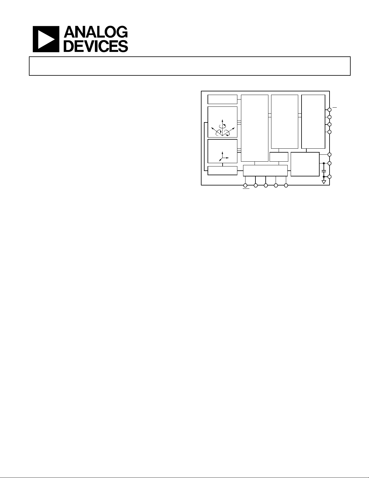
FUNCTIONAL BLOCK DIAGRAM
TEMPERATURE
SENSOR
TRIAXIS MEMS
ANGULAR RATE
SENSOR
TRIAXIS MEMS
ACCELERATIO N
SENSOR
SELF-TEST
ADIS16375
SIGNAL
CONDITIO NING
AND
CONVERSION
DIGITAL
CONTROL
RST
CALIBRATION
DIGITAL
PROCESSING
ALARMS
DIO3DIO2DIO1
Figure 1.
AND
DIO4
OUTPUT
REGISTERS
AND SPI
INTERFACE
POWER
MANAGEMENT
GENERAL DESCRIPTION
The ADIS16375 iSensor® is a complete inertial system that includes
a triaxis gyroscope and triaxis accelerometer. Each sensor in the
ADIS16375 combines industry-leading iMEMS® technology
with signal conditioning that optimizes dynamic performance.
The factory calibration characterizes each sensor for sensitivity,
bias, alignment, and linear acceleration (gyro bias). As a result,
each sensor has its own dynamic compensation formulas that
provide accurate sensor measurements over a temperature
range of −40°C to +85°C.
The ADIS16375 provides a simple, cost-effective method for
integrating accurate, multiaxis, inertial sensing into industrial
systems, especially when compared with the complexity and
investment associated with discrete designs. All necessary motion
testing and calibration are part of the production process at the
factory, greatly reducing system integration time. Tight orthogonal
alignment simplifies inertial frame alignment in navigation systems.
An improved SPI interface and register structure provide faster
data collection and configuration control.
This compact module is approximately 44 mm × 47 mm × 14 mm
and provides a flexible connector interface that enables multiple
mounting orientation options.
CS
SCLK
DIN
DOUT
VDDRTC
VCC
GND
09389-001
Rev. B
Information furnished by Analog Devices is believed to be accurate and reliable. However, no
responsibility is assumed by Anal og Devices for its use, nor for any infringements of patents or ot her
rights of third parties that may result from its use. Specifications subject to change without notice. No
license is granted by implication or otherwise under any patent or patent rights of Analog Devices.
Trademarks and registered trademarks are the property of their respective owners.
One Technology Way, P.O. Box 9106, Norwood, MA 02062-9106, U.S.A.
Tel: 781.329.4700 www.analog.com
Fax: 781.461.3113 ©2010–2011 Analog Devices, Inc. All rights reserved.

ADIS16375
TABLE OF CONTENTS
Features.............................................................................................. 1
Applications....................................................................................... 1
Functional Block Diagram .............................................................. 1
General Description ......................................................................... 1
Revision History ............................................................................... 2
Specifications..................................................................................... 3
Timing Specifications .................................................................. 5
Absolute Maximum Ratings............................................................ 6
ESD Caution.................................................................................. 6
Pin Configuration and Function Descriptions............................. 7
Typical Performance Characteristics ............................................. 8
Basic Operation................................................................................. 9
Register Structure......................................................................... 9
SPI Communication................................................................... 10
Device Configuration ................................................................ 10
Reading Sensor Data.................................................................. 10
User Registers.................................................................................. 11
Output Data Registers.................................................................... 13
Digital Signal Processing............................................................... 17
Sampling Plan............................................................................. 17
Averaging/Decimation Filter.................................................... 17
FIR Filter Banks.......................................................................... 17
Calibration....................................................................................... 19
Alarms.............................................................................................. 22
System Controls.............................................................................. 23
Global Commands ..................................................................... 23
Memory Management............................................................... 23
General-Purpose I/O ................................................................. 24
Power Management ................................................................... 24
Applications Information.............................................................. 26
Prototype Interface Board ......................................................... 26
Installation Tips.......................................................................... 26
Outline Dimensions....................................................................... 27
Ordering Guide .......................................................................... 27
REVISION HISTORY
7/11—Rev. A to Rev. B
Changes to Accelerometers, Nonlinearity Parameter and Power
Supply, VDD Parameter in Table 1................................................. 3
Changes to t
Changed Angular Displacement Heading to Delta Angles ...... 14
Changes to Delta Angles Section.................................................. 14
Changes to Table 28 and Velocity Changes Section................... 15
Change to Figure 18 ....................................................................... 17
Changes to Data-Ready Indicator Section and Input Sync/Clock
Control Section............................................................................... 24
Moved Real-Time Clock Configuration/Data Section, Table 96,
Table 97, and Table 98.................................................................... 25
Changes to Real-Time Clock Configuration/Data Section ...... 25
Changes to Prototype Interface Board Section........................... 26
, t
, t2, and t3 Parameters in Table 2................... 5
CLS
CHS
2/11—Rev. 0 to Rev. A
Changes to Gyroscopes Misalignment and Accelerometers
Misalignment Test Conditions/Comments, Table 1.....................3
Added Endnote 7...............................................................................4
Changes to Table 54 and Table 55 ................................................ 17
Changes to Table 57, Table 58, and Table 59............................... 18
10/10—Revision 0: Initial Version
Rev. B | Page 2 of 28

ADIS16375
SPECIFICATIONS
TA = 25°C, VDD = 3.3 V, angular rate = 0°/sec, dynamic range = ±300°/sec ± 1 g, unless otherwise noted.
Table 1.
Parameter Test Conditions/Comments Min Typ Max Unit
GYROSCOPES
Dynamic Range ±300 ±350 °/sec
Sensitivity1 16-bit resolution, x_GYRO_OUT registers only 0.01311 °/sec/LSB
Initial Sensitivity Tolerance ±1 %
Sensitivity Temperature Coefficient −40°C ≤ TA ≤ +85°C ±40 ppm/°C
Misalignment Axis-to-axis ±0.05 Degrees
Axis-to-frame (package) ±1.0 Degrees
Nonlinearity Best-fit straight line ±0.025 % of FS
Initial Bias Error ±1 σ ±1.0 °/sec
In-Run Bias Stability 1 σ 12 °/hr
Angular Random Walk 1 σ 1.0 °/√hr
Bias Temperature Coefficient −40°C ≤ TA ≤ +85°C ±0.005 °/sec/°C
Linear Acceleration Effect on Bias Any axis, 1 σ (GEN_CONFIG[7] = 1) ±0.013 °/sec/g
Output Noise No filtering 0.45 °/sec rms
Rate Noise Density f = 25 Hz, no filtering 0.02 °/sec/√Hz rms
3 dB Bandwidth 330 Hz
Sensor Resonant Frequency 14.5 kHz
ACCELEROMETERS Each axis
Dynamic Range ±18
Sensitivity1 16-bit resolution, x_ACCL_OUT registers only 0.8192 mg/LSB
Initial Sensitivity Tolerance ±1 %
Sensitivity Temperature Coefficient −40°C ≤ TA ≤ +85°C ±25 ppm/°C
Misalignment Axis-to-axis ±0.035 Degrees
Axis-to-frame (package) ±1.0 Degrees
Nonlinearity Best-fit straight line, ±10 g ±0.1 % of FS
Best-fit straight line, ±18 g ±0.5 % of FS
Initial Bias Error ±1 σ ±16 mg
In-Run Bias Stability 1 σ 0.13 mg
Velocity Random Walk 1 σ 0.076 m/sec/√hr
Bias Temperature Coefficient −40°C ≤ TA ≤ +85°C ±0.1 mg/°C
Output Noise No filtering 1.5 mg rms
Noise Density No filtering 0.06 mg/√Hz rms
3 dB Bandwidth 330 Hz
Sensor Resonant Frequency 5.5 kHz
TEMPERATURE SENSOR
Scale Factor Output = 0x0000 at 25°C (±5°C) 0.00565 °C/LSB
LOGIC INPUTS2
Input High Voltage, VIH 2.0 V
Input Low Voltage, VIL 0.8 V
CS Wake-Up Pulse Width
Logic 1 Input Current, IIH V
Logic 0 Input Current, IIL V
All Pins Except RST
RST Pin
Input Capacitance, CIN 10 pF
DIGITAL OUTPUTS
Output High Voltage, VOH I
Output Low Voltage, VOL I
20 μs
= 3.3 V 10 μA
IH
= 0 V
IL
10 μA
0.33 mA
= 0.5 mA 2.4 V
SOURCE
= 2.0 mA 0.4 V
SINK
g
Rev. B | Page 3 of 28

ADIS16375
Parameter Test Conditions/Comments Min Typ Max Unit
FLASH MEMORY Endurance3 100,000 Cycles
Data Retention4 T
FUNCTIONAL TIMES5 Time until data is available
Power-On Startup Time 500 ms
Reset Recovery Time 500 ms
Sleep Mode Recovery Time 500 μs
Flash Memory Update Time 375 ms
Flash Memory Test Time 50 ms
Automatic Self Test Time Using internal clock, 100 SPS 10 ms
CONVERSION RATE 2.46 kSPS
Initial Clock Accuracy 0.02 %
Temperature Coefficient 40 ppm/°C
Sync Input Clock 0.76 2.25 kHz
POWER SUPPLY, VDD Operating voltage range 3.0 3.6 V
Power Supply Current7 Normal mode, VDD = 3.3 V 173 mA
Sleep mode, VDD = 3.3 V 12.3 mA
Power-down mode, VDD = 3.3 V 120 μA
POWER SUPPLY, VDDRTC Operating voltage range 3.3 V
Real-Time Clock Supply Current Normal mode, VDDRTC = 3.3 V 13 μA
1
Each gyroscope and accelerometer has 32 bits of available resolution. The 16-bit sensitivity shown reflects the register that contains the upper 16 bits of the sensor
output. Divide this number by 2 for every bit added to this resolution in downstream processing routines.
2
The digital I/O signals are driven by an internal 3.3 V supply, and the inputs are 5 V tolerant.
3
Endurance is qualified as per JEDEC Standard 22, Method A117, and measured at −40°C, +25°C, +85°C, and +125°C.
4
The data retention lifetime equivalent is at a junction temperature (TJ) of 85°C as per JEDEC Standard 22, Method A117. Data retention lifetime decreases with junction
temperature.
5
These times do not include thermal settling and internal filter response times (330 Hz bandwidth), which may affect overall accuracy.
6
The 0.7 kHz lower limit is established to support Nyquist sampling criteria for the 330 Hz sensor bandwidth.
7
During startup, the power supply current increases and experiences transient behaviors for a period of 400 μs. The peak current during the 400 μs transient period can
reach 1500 mA.
= 85°C 20 Years
J
Rev. B | Page 4 of 28
ADIS16375
C
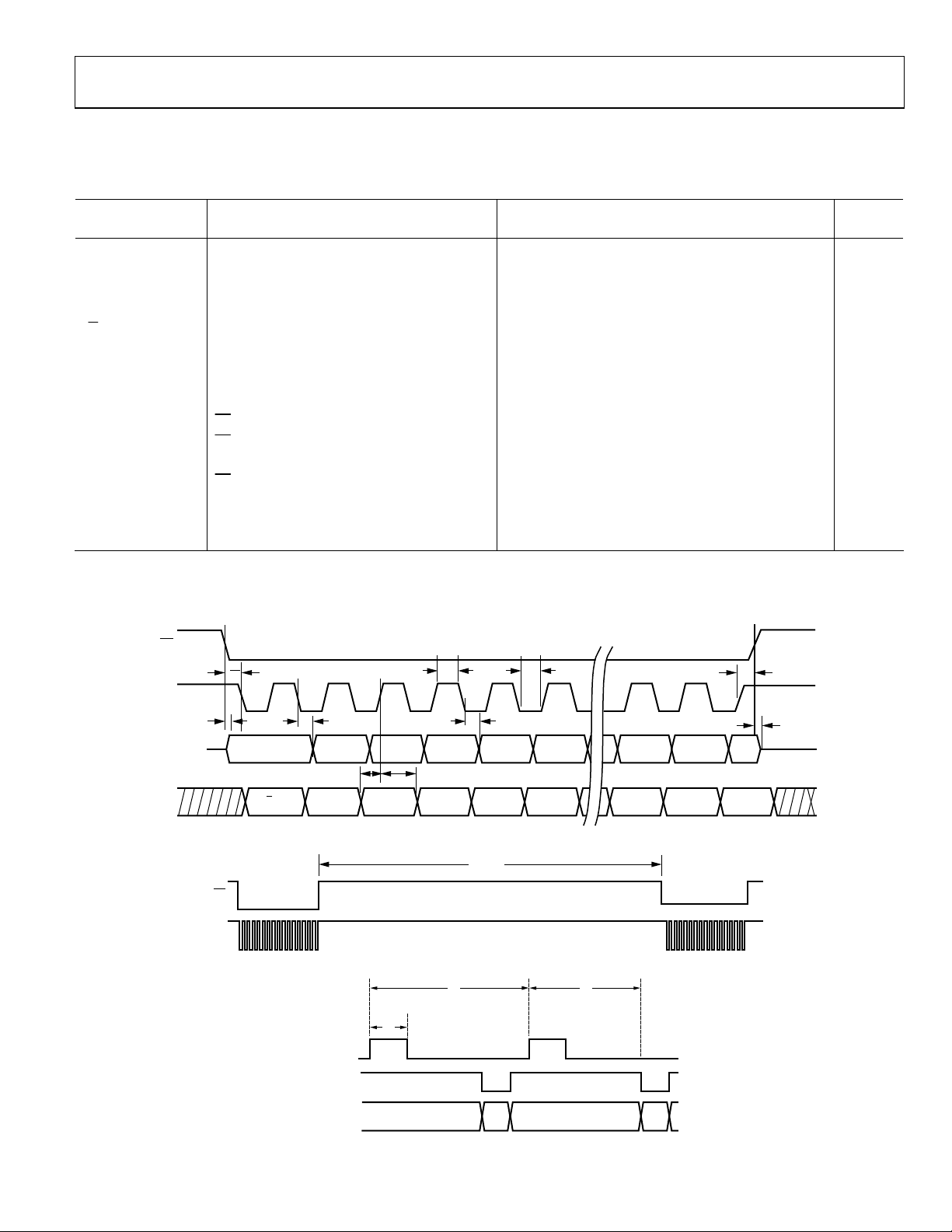
TIMING SPECIFICATIONS
TA = 25°C, VDD = 3.3 V, unless otherwise noted.
Table 2.
Normal Mode
Parameter Description Min1 Typ Max Unit
f
Serial clock 0.01 15 MHz
SCLK
t
Stall period between data 2 μs
STALL
t
Serial clock low period 31 ns
CLS
t
Serial clock high period 31 ns
CHS
tCS Chip select to clock edge 32 ns
t
DOUT valid after SCLK edge 10 ns
DAV
t
DIN setup time before SCLK rising edge 2 ns
DSU
t
DIN hold time after SCLK rising edge 2 ns
DHD
tDR, tDF DOUT rise/fall times, ≤100 pF loading 3 8 ns
t
t
SFS
DSOE
high after SCLK edge
CS
assertion to data out active
CS
tHD SCLK edge to data out invalid 0 ns
t
DSHI
t
1
t
2
t
3
1
Guaranteed by design and characterization but not tested in production.
deassertion to data out high impedance
CS
Input sync pulse width 5 μs
Input sync to data-ready output 490 μs
Input sync period 500 μs
Timing Diagrams
32 ns
0 11 ns
0 9 ns
CS
SCLK
DOUT
DIN
CS
SCLK
t
t
CS
1 2 3 4 5 6 15 16
t
DSOE
MSB DB14
R/W A5A6 A4 A3 A2
t
DAV
t
DSU
CHS
t
HD
DB13 DB12 DB10DB11 DB2 LSBDB1
t
DHD
t
CLS
D2
Figure 2. SPI Timing and Sequence
t
STALL
Figure 3. Stall Time and Data Rate
SYNC
LOCK (CLKIN)
DATA
READY
OUTPUT
REGISTERS
t
3
t
1
DATA VALID DATA VALID
t
2
Figure 4. Input Clock Timing Diagram
Rev. B | Page 5 of 28
D1 LSB
09389-004
t
SFS
t
DSHI
09389-002
09389-003
ADIS16375
ABSOLUTE MAXIMUM RATINGS
Table 3.
Parameter Rating
Acceleration
Any Axis, Unpowered 2000 g
Any Axis, Powered 2000 g
VCC to GND −0.3 V to +3.6 V
Digital Input Voltage to GND −0.3 V to +3.6 V
Digital Output Voltage to GND −0.3 V to +3.6 V
Operating Temperature Range −40°C to +85°C
Storage Temperature Range −65°C to +150°C
1
Extended exposure to temperatures outside the specified temperature
range of −40°C to +85°C can adversely affect the accuracy of the factory
calibration. For best accuracy, store the parts within the specified operating
range of −40°C to +85°C.
1
Stresses above those listed under Absolute Maximum Ratings
may cause permanent damage to the device. This is a stress
rating only; functional operation of the device at these or any
other conditions above those indicated in the operational
section of this specification is not implied. Exposure to absolute
maximum rating conditions for extended periods may affect
device reliability.
Table 4. Package Characteristics
Package Type θJA θJC Device Weight
24-Lead Module (ML-24-3) 20.5 6.3 25 g
ESD CAUTION
Rev. B | Page 6 of 28
ADIS16375
A
PIN CONFIGURATION AND FUNCTION DESCRIPTIONS
DIS16375
TOP VIEW
(Not to Scale)
DIO4
DOUT
CS
RST
VDD
VDD
GND
DNC
DNC
DNC
DNC
DNC
10
12
14
16
18
20
22
24
2
11
13
15
17
19
21
23
DNC
VDDRTC
NOTES
1. THIS REPRESENTATION DISPLAYS THE TOP VIEW PINOUT
FOR THE MATI NG SO CKET CO NNECTO R.
2. THE ACTUAL CONNECTOR PI NS ARE NOT VI SIBLE FROM
THE TOP VIEW .
3. MATING CONNECTOR: S AMTEC CLM-112- 02 OR EQUIVAL ENT.
4. DNC = DO NOT CONNECT.
GND
DNC
DNC
VDD
GND
DIO2
3456789
1
DIN
DIO1
DIO3
SCLK
09389-005
Figure 5. Mating Connector Pin Assignments
PIN 23
PIN 1
09389-006
Figure 6. Axial Orientation (Top Side Facing Up)
Table 5. Pin Function Descriptions
Pin No. Mnemonic Typ e Description
1 DIO3 Input/Output Configurable Digital Input/Output.
2 DIO4 Input/Output Configurable Digital Input/Output.
3 SCLK Input SPI Serial Clock.
4 DOUT Output SPI Data Output. Clocks output on SCLK falling edge.
5 DIN Input SPI Data Input. Clocks input on SCLK rising edge.
6
CS
Input SPI Chip Select.
7 DIO1 Input/Output Configurable Digital Input/Output.
8
RST
Input Reset.
9 DIO2 Input/Output Configurable Digital Input/Output.
10, 11, 12 VDD Supply Power Supply.
13, 14, 15 GND Supply Power Ground.
16 to 22, 24 DNC Not applicable Do Not Connect.
23 VDDRTC Supply Real-Time Clock Power Supply.
Rev. B | Page 7 of 28
ADIS16375
TYPICAL PERFORMANCE CHARACTERISTICS
1000
100
AVERAGE
0.001
AVERAGE
+1σ
10
ALLAN VARIANCE (°/ Hour)
1
0.01 0.1 1 10 100 1000 10000
INTEGRATION PERIOD (Seconds)
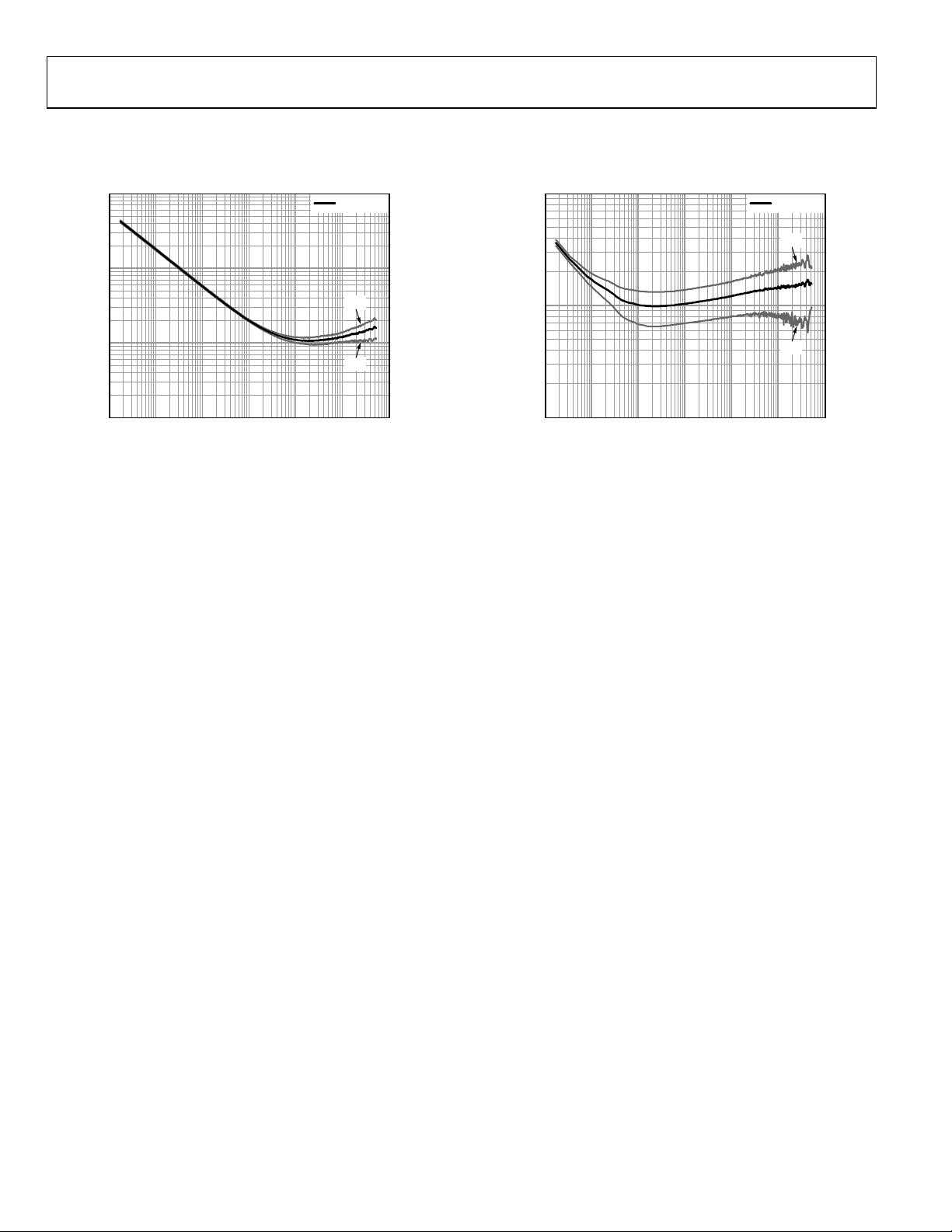
Figure 7. Gyroscope Allan Variance, +25°C
+1σ
–1σ
0.0001
ALLAN VARIANCE ( g)
0.00001
0.01 0.1 1 10 100 1000 10000
09389-007
INTEGRATION PERIOD (Seconds)
–1σ
09389-008
Figure 8. Accelerometer Allan Variance, 25°C
Rev. B | Page 8 of 28
ADIS16375
BASIC OPERATION
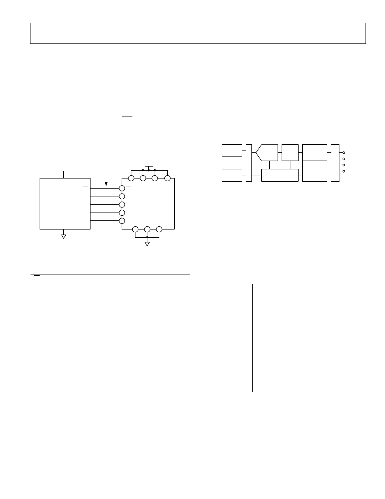
The ADIS16375 is an autonomous sensor system that starts up
on its own when it has a valid power supply. After running through
its initialization process, it begins sampling, processing, and
loading calibrated sensor data into the output registers, which
are accessible using the SPI port. The SPI port typically connects to
a compatible port on an embedded processor, using the connection
diagram in Figure 9. The four SPI signals facilitate synchronous,
serial data communication. Connect
RST
Tabl e 5
(see ) to VDD
or leave it open for normal operation. The factory default
configuration provides users with a data-ready signal on the
DIO2 pin, which pulses high when new data is available in the
output data registers.
VDD
SYSTEM
PROCESSOR
SPI MASTER
I/O LI NES ARE COMPATIBLE WI TH
3.3V LOG IC LEVE LS
SS
SCLK
MOSI
MISO
IRQ DIO2
Figure 9. Electrical Connection Diagram
6
3
5
4
9
10
CS
SCLK
DIN
DOUT
13 14 15
+3.3V
11 12 23
ADIS16375
09389-010
Table 6. Generic Master Processor Pin Names and Functions
Mnemonic Function
SS
Slave select
IRQ Interrupt request
MOSI Master output, slave input
MISO Master input, slave output
SCLK Serial clock
Embedded processors typically use control registers to configure
their serial ports for communicating with SPI slave devices,
such as the ADIS16375. Tabl e 7 provides a list of settings, which
describe the SPI protocol of the ADIS16375. The initialization
routine of the master processor typically establishes these settings
using firmware commands to write them into its serial control
registers.
Table 7. Generic Master Processor SPI Settings
Processor Setting Description
Master The ADIS16375 operates as a slave.
SCLK ≤ 15 MHz Maximum serial clock rate.
SPI Mode 3 CPOL = 1 (polarity), and CPHA = 1 (phase).
MSB-First Mode Bit sequence.
16-Bit Mode Shift register/data length.
REGISTER STRUCTURE
The register structure and SPI port provide a bridge between
the sensor processing system and an external, master processor.
It contains both output data and control registers. The output
data registers include the latest sensor data, a real-time clock, error
flags, alarm flags, and identification data. The control registers
include sample rate, filtering, input/output, alarms, calibration,
and diagnostic configuration options. All communication
between the ADIS16375 and an external processor involves
either reading or writing to one of the user registers.
TRIAXIS
GYRO
TRIAXIS
ACCEL
TEMP
SENSOR
CONTROLL ER
Figure 10. Basic Operation
DSP
The register structure uses a paged addressing scheme that is
comprised of 13 pages, with each one containing 64 register
locations. Each register is 16-bits wide, with each byte having its
own unique address within that page’s memory map. The SPI
port has access to one page at a time, using the bit sequences in
Figure 15. Select the page to activate for SPI access by writing its
code to the PAGE_ID register. Read the PAGE_ID register to
determine which page is currently active. Ta b le 8 displays the
PAGE_ID contents for each page, along with their basic function.
The PAGE_ID register is located at Address 0x00 on every page.
Table 8. User Register Page Assignments
Page PAGE_ID Function
0 0x00 Output data, clock, identification
1 0x01 Reserved
2 0x02
3 0x03
4 0x04
5 0x05
6 0 x06
7 0x07
8 0 x08
9 0x09
10 0x0A
11 0x0B
Calibration
Control: sample rate, filtering, I/O, alarms
Reserved
FIR Filter Bank A Coefficients, 1 to 60
FIR Filter Bank A, Coefficients, 61 to 120
FIR Filter Bank B, Coefficients, 1 to 60
FIR Filter Bank B, Coefficients, 61 to 120
FIR Filter Bank C, Coefficients, 1 to 60
FIR Filter Bank C, Coefficients, 61 to 120
FIR Filter Bank D, Coefficients, 1 to 60
12 0x0C FIR Filter Bank D, Coefficients, 61 to 120
OUTPUT
REGISTERS
CONTROL
REGISTERS
SPI
09389-011
Rev. B | Page 9 of 28

ADIS16375
2
SPI COMMUNICATION
The SPI port supports full duplex communication, as shown in
Figure 15, which enables external processors to write to DIN
while reading DOUT, if the previous command was a read
request. Figure 15 provides a guideline for the bit coding on
both DIN and DOUT.
DEVICE CONFIGURATION
The SPI provides write access to the control registers, one byte at
a time, using the bit assignments shown in Figure 15. Each register
has 16 bits, where Bits[7:0] represent the lower address (listed in
Tabl e 9 ) and Bits[15:8] represent the upper address. Write to the
lower byte of a register first, followed by a write to its upper byte
second. The only register that changes with a single write to its
lower byte is the PAGE_ID register. For a write command, the
first bit in the DIN sequence is set to 1. The Address Bits[A6:A0]
represent the target address and the Data Command Bits[DC7:DC0]
represent the data being written to the location. Figure 11
provides an example of writing 0x03 to Address 0x00
(PAGE_ID[7:0]), using DIN = 0x8003. This write command
activates the control page for SPI access.
CS
SCLK
DIN
DIN = 1000 0000 0000 0011 = 0x8003, WRITE S 0x03 TO ADDRESS 0x00
Figure 11. SPI Sequence for Activating the Control Page (DIN = 0x8003)
Dual Memory Structure
Writing configuration data to a control register updates its SRAM
contents, which are volatile. After optimizing each relevant control
register setting in a system, use the manual flash update command,
which is located in GLOB_CMD[3] on Page 3 of the register map.
Activate the manual flash update command by turning to Page 3
(DIN = 0x8003) and setting GLOB_CMD[3] = 1 (DIN = 0x8204,
then DIN = 0x8300). Make sure that the power supply is within
specification for the entire 375 ms processing time for a flash
memory update. Ta ble 9 provides a memory map for all of
the user registers, which includes a column of flash backup
information. A yes in this column indicates that a register
has a mirror location in flash and, when backed up properly,
automatically restores itself during startup or after a reset.
Figure 12 provides a diagram of the dual memory structure
used to manage operation and store critical user settings.
9389-012
NONVOLATILE
FLASH MEMO RY
(NO SPI ACCESS )
Figure 12. SRAM and Flash Memory Diagram
READING SENSOR DATA
The ADIS16375 automatically starts up and activates Page 0 for
data register access. Write 0x00 to the PAGE_ID register (DIN =
0x8000) to activate Page 0 for data access after accessing any other
page. A single register read requires two 16-bit SPI cycles. The
first cycle requests the contents of a register using the bit assignments
in Figure 15, and then the register contents follow DOUT during
the second sequence. The first bit in a DIN command is zero,
followed by either the upper or lower address for the register.
The last eight bits are don’t care, but the SPI requires the full set
of 16 SCLKs to receive the request. Figure 13 includes two register
reads in succession, which starts with DIN = 0x1A00 to request
the contents of the Z_GYRO_OUT register and follows with
0x1800 to request the contents of the Z_GYRO_LOW register.
DIN
DOUT
Figure 14 provides an example of the four SPI signals when reading
PROD_ID in a repeating pattern. This is a good pattern to use
for troubleshooting the SPI interface setup and communications
because the contents of PROD_ID are predefined and stable.
CS
SCLK
DIN
DOUT
DOUT = 0011 1111 1111 0111 = 0x3FF7 = 16,375 (PROD_ID)
0x1A00 0x1800
Figure 14. SPI Read Example, Second 16-Bit Sequence
MANUAL
FLASH
BACKUP
VOLATILE
SRAM
SPI ACCESS
START-UP
RESET
Z_GYRO_OUT Z_GYRO_LOW
Figure 13. SPI Read Example
DIN = 0111 1110 0000 0000 = 0x7E00
NEXT
ADDRESS
09389-013
09389-014
09389-015
CS
SCLK
R/W
DIN
DOUT
NOTES
1. DOUT BITS ARE PRO DUCED ONLY WHEN THE PREVIOUS 16-BIT DIN SEQUENCE STARTS WI TH R/W = 0.
. WHEN CS IS HIGH, DOUT IS IN A THREE-STAT E, HIGH I MPEDANCE MODE, WHICH ALLOWS MULT IFUNCTIONAL USE OF THE LINE
FOR OTHER DEVICES.
R/W
A6 A5 A4 A3 A2 A1 A0 DC7 DC6 DC5 DC4 DC3 DC2 DC1 DC0
D0D1D2D3D4D5D6D7D8D9D10D11D12D13D14D15
A6 A5
D13D14D15
09389-016
Figure 15. SPI Communication Bit Sequence
Rev. B | Page 10 of 28

ADIS16375
USER REGISTERS
Table 9. User Register Memory Map (N/A = Not Applicable)
Name R/W Flash PAGE_ID Address Default Register Description Format
PAGE_ID R/W No 0x00 0x00 0x00 Page Identifier N/A
Reserved N/A N/A 0x00 0x02 to 0x07 N/A Reserved N/A
SYS_E_FLAG R No 0x00 0x08 0x0000 Output, system error flags Table 41
DIAG_STS R No 0x00 0x0A 0x0000 Output, self test error flags Table 42
ALM_STS R No 0x00 0x0C 0x0000 Output, alarm error flags Table 43
TEMP_OUT R No 0x00 0x0E N/A Output, temperature Table 39
X_GYRO_LOW R No 0x00 0x10 N/A Output, x-axis gyroscope, low word Table 15
X_GYRO_OUT R No 0x00 0x12 N/A Output, x-axis gyroscope, high word Table 11
Y_GYRO_LOW R No 0x00 0x14 N/A Output, y-axis gyroscope, low word Table 16
Y_GYRO_OUT R No 0x00 0x16 N/A Output, y-axis gyroscope, high word Table 12
Z_GYRO_LOW R No 0x00 0x18 N/A Output, z-axis gyroscope, low word Table 17
Z_GYRO_OUT R No 0x00 0x1A N/A Output, z-axis gyroscope, high word Table 13
X_ACCL_LOW R No 0x00 0x1C N/A Output, x-axis accelerometer, low word Table 22
X_ACCL_OUT R No 0x00 0x1E N/A Output, x-axis accelerometer, high word Table 18
Y_ACCL_LOW R No 0x00 0x20 N/A Output, y-axis accelerometer, low word Table 23
Y_ACCL_OUT R No 0x00 0x22 N/A Output, y-axis accelerometer, high word Table 19
Z_ACCL_LOW R No 0x00 0x24 N/A Output, z-axis accelerometer, low word Table 24
Z_ACCL_OUT R No 0x00 0x26 N/A Output, z-axis accelerometer, high word Table 20
Reserved N/A N/A 0x00 0x28 to 0x3F N/A Reserved N/A
X_DELTA_ANG_L R No 0x00 0x40 N/A Output, x-axis delta angle, low word Table 29
X_DELTA_ANG_H R No 0x00 0x42 N/A Output, x-axis delta angle, high word Table 25
Y_DELTA_ANG_L R No 0x00 0x44 N/A Output, y-axis delta angle, low word Table 30
Y_DELTA_ANG_H R No 0x00 0x46 N/A Output, y-axis delta angle, high word Table 26
Z_DELTA_ANG_L R No 0x00 0x48 N/A Output, z-axis delta angle, low word Table 31
Z_DELTA_ANG_H R No 0x00 0x4A N/A Output, z-axis delta angle, high word Table 27
X_DELTA_VEL_L R No 0x00 0x4C N/A Output, x-axis delta velocity, low word Table 36
X_DELTA_VEL_H R No 0x00 0x4E N/A Output, x-axis delta velocity, high word Table 32
Y_DELTA_VEL_L R No 0x00 0x50 N/A Output, y-axis delta velocity, low word Table 37
Y_DELTA_VEL_H R No 0x00 0x52 N/A Output, y-axis a delta velocity, high word Table 33
Z_DELTA_VEL_L R No 0x00 0x54 N/A Output, z-axis delta velocity, low word Table 38
Z_DELTA_VEL_H R No 0x00 0x56 N/A Output, z-axis delta velocity, high word Table 34
Reserved N/A N/A 0x00 0x58 to 0x6F N/A Reserved N/A
TIME_MS_OUT R/W Yes 0x00 0x70 N/A Output, time, minutes, and seconds Table 96
TIME_DH_OUT R/W Yes 0x00 0x72 N/A Output, time, days, and hours Table 97
TIME_YM_OUT R/W Yes 0x00 0x74 N/A Output, time, years, and months Table 98
Reserved N/A N/A 0x00 0x76 N/A Reserved N/A
LOT_ID1 R Yes 0x00 0x78 N/A Output, lot identification number Table 44
LOT_ID2 R Yes 0x00 0x7A N/A Output, lot identification number Table 45
LOT_ID3 R Yes 0x00 0x7C N/A Output, lot identification number Table 46
PROD_ID R Yes 0x00 0x7E 0x3FF7 Output, product identification (16,375) Table 47
Reserved N/A N/A 0x01 0x00 to 0x7F N/A Reserved N/A
PAGE_ID R/W No 0x02 0x00 0x00 Page identifier N/A
Reserved N/A N/A 0x02 0x02 to 0x0E N/A Reserved N/A
XGYRO_OFF_L R/W Yes 0x02 0x10 0x0000 Calibration, offset, x-axis gyroscope, low word Table 62
XGYRO_OFF_H R/W Yes 0x02 0x12 0x0000 Calibration, offset, x-axis gyroscope, high word Table 59
YGYRO_OFF_L R/W Yes 0x02 0x14 0x0000 Calibration, offset, y-axis gyroscope, low word Table 63
YGYRO_OFF_H R/W Yes 0x02 0x16 0x0000 Calibration, offset, y-axis gyroscope, high word Table 60
ZGYRO_OFF_L R/W Yes 0x02 0x18 0x0000 Calibration, offset, z-axis gyroscope, low word Table 64
ZGYRO_OFF_H R/W Yes 0x02 0x1A 0x0000 Calibration, offset, z-axis gyroscope, high word Table 61
XACCL_OFF_L R/W Yes 0x02 0x1C 0x0000 Calibration, offset, x-axis accelerometer, low word Table 68
XACCL_OFF_H R/W Yes 0x02 0x1E 0x0000 Calibration, offset, x-axis accelerometer, high word Table 65
Rev. B | Page 11 of 28

ADIS16375
Name R/W Flash PAGE_ID Address Default Register Description Format
YACCL_OFF_L R/W Yes 0x02 0x20 0x0000 Calibration, offset, y-axis accelerometer, low word Table 69
YACCL_OFF_H R/W Yes 0x02 0x22 0x0000 Calibration, offset, y-axis accelerometer, high word Table 66
ZACCL_OFF_L R/W Yes 0x02 0x24 0x0000 Calibration, offset, z-axis accelerometer, low word Table 70
ZACCL_OFF_H R/W Yes 0x02 0x26 0x0000 Calibration, offset, z-axis accelerometer, high word Table 67
Reserved N/A N/A 0x02 0x28 to 0x3E N/A Reserved N/A
XGYRO_SCL R/W Yes 0x02 0x40 0x0000 Calibration, scale, x-axis gyroscope Table 71
YGYRO_SCL R/W Yes 0x02 0x42 0x0000 Calibration, scale, y-axis gyroscope Table 72
ZGYRO_SCL R/W Yes 0x02 0x44 0x0000 Calibration, scale, z-axis gyroscope Table 73
XACCL_SCL R/W Yes 0x02 0x46 0x0000 Calibration, scale, x-axis accelerometer Table 74
YACCL_SCL R/W Yes 0x02 0x48 0x0000 Calibration, scale, y-axis accelerometer Table 75
ZACCL_SCL R/W Yes 0x02 0x4A 0x0000 Calibration, scale, z-axis accelerometer Table 76
Reserved N/A N/A 0x02 0x4C to 0x67 N/A Reserved N/A
SERIAL_NUM R Yes 0x02 0x68 N/A Serial number Table 48
Reserved N/A N/A 0x02 0x6Ato 0x77 N/A Reserved N/A
FLSH_CNT_L R Yes 0x02 0x78 N/A Diagnostic, flash memory write count, low word Table 91
FLSH_CNT_H R Yes 0x02 0x7A N/A Diagnostic, flash memory write count, high word Table 92
Reserved N/A N/A 0x02 0x7C to 0x7F N/A Reserved N/A
PAGE_ID R/W No 0x03 0x00 0x0000 Page identifier N/A
GLOB_CMD W No 0x03 0x02 N/A Control, global commands Table 90
Reserved N/A N/A 0x03 0x04 N/A Reserved N/A
FNCIO_CTRL R/W Yes 0x03 0x06 0x000D Control, I/O pins, functional definitions Table 93
GPIO_CTRL R/W Yes 0x03 0x08 0x0000 Control, I/O pins, general purpose Table 94
GEN_CONFIG R/W Yes 0x03 0x0A 0x00C0 Control, clock and miscellaneous correction Table 78
DEC_RATE R/W Yes 0x03 0x0C Control, output sample rate decimation Table 50
NULL_CFG R/W Yes 0x03 0x0E 0x070B Control, automatic bias correction configuration Table 77
SLP_CFG R/W No 0x03 0x10 N/A Control, power-down/sleep mode Table 95
Reserved N/A N/A 0x03 0x12 to 0x15 N/A Reserved N/A
FILTER_SEL1 R/W Yes 0x03 0x16 0x0000 Filter selection Table 51
FILTER_SEL2 R/W Yes 0x03 0x18 0x0000 Filter selection Table 52
Reserved N/A N/A 0x03 0x1A to 0x1F N/A Reserved N/A
ALM_CONFIG_1 R/W Yes 0x03 0x20 0x0000 Alarm configuration Table 86
ALM_CONFIG_2 R/W Yes 0x03 0x22 0x0000 Alarm configuration Table 87
Reserved N/A N/A 0x03 0x24 to 0x3E N/A Reserved N/A
XG_ALM_MAG R/W Yes 0x03 0x40 0x0000 X-axis gyroscope alarm trigger level Table 80
YG_ALM_MAG R/W Yes 0x03 0x42 0x0000 Y-axis gyroscope alarm trigger level Table 81
ZG_ALM_MAG R/W Yes 0x03 0x44 0x0000 Z-axis gyroscope alarm trigger level Table 82
XA_ALM_MAG R/W Yes 0x03 0x46 0x0000 X-axis accelerometer alarm trigger level Table 83
YA_ALM_MAG R/W Yes 0x03 0x48 0x0000 Y-axis accelerometer alarm trigger level Table 84
ZA_ALM_MAG R/W Yes 0x03 0x4A 0x0000 Z-axis accelerometer alarm trigger level Table 85
Reserved N/A N/A 0x03 0x4C to 0x7F N/A Reserved N/A
Reserved N/A N/A 0x04 0x00 to 0x7F N/A Reserved N/A
FIR_COEF_Axxx R/W Yes 0x05 0x00 to 0x7F N/A FIR Filter Bank A, Coefficients 1 through 60 Table 53
FIR_COEF_Axxx R/W Yes 0x06 0x00 to 0x7F N/A FIR Filter Bank A, Coefficients 61 through 120 Table 53
FIR_COEF_Bxxx R/W Yes 0x07 0x00 to 0x7F N/A FIR Filter Bank B, Coefficients 1 through 60 Table 54
FIR_COEF_Bxxx R/W Yes 0x08 0x00 to 0x7F N/A FIR Filter Bank B, Coefficients 61 through 120 Table 54
FIR_COEF_Cxxx R/W Yes 0x09 0x00 to 0x7F N/A FIR Filter Bank C, Coefficients 1 through 60 Table 55
FIR_COEF_Cxxx R/W Yes 0x0A 0x00 to 0x7F N/A FIR Filter Bank C, Coefficients 61 through 120 Table 55
FIR_COEF_Dxxx R/W Yes 0x0B 0x00 to 0x7F N/A FIR Filter Bank D, Coefficients 1 through 60 Table 56
FIR_COEF_Dxxx R/W Yes 0x0C 0x00 to 0x7F N/A FIR Filter Bank D, Coefficients 61 through 120 Table 56
Rev. B | Page 12 of 28

ADIS16375
Y
X
OUTPUT DATA REGISTERS
After the ADIS16375 completes its startup process, the PAGE_ID
register contains 0x0000, which sets Page 0 as the active page
for SPI access. Page 0 contains the output data, real-time clock,
status and product identification registers.
Table 10. Output Data Register Summary
Register Address
Measurement
SYS_E_FLAG 0x08 System flags
DIAG_STS 0x0A Self test flags
ALM_STS 0x0C
TEMP_OUT 0x0E
X_GYRO_LOW 0x10
Alarm flags
Temperature
Gyroscope, X
X_GYRO_OUT 0x12 Gyroscope, X
Y_GYRO_LOW 0x14
Y_GYRO_OUT 0x16
Z_GYRO_LOW 0x18
Z_GYRO_OUT 0x1A
X_ACCL_LOW 0x1C
X_ACCL_OUT 0x1E
Y_ACCL_LOW 0x20
Y_ACCL_OUT 0x22
Gyroscope, Y
Gyroscope, Y
Gyroscope, Z
Gyroscope, Z
Accelerometer, X
Accelerometer, X
Accelerometer, Y
Accelerometer, Y
Z_ACCL_LOW 0x24 Accelerometer, Z
Z_ACCL_OUT 0x26 Accelerometer, Z
X_DELTA_ANG_L 0x40 Delta angle, X
X_DELTA_ANG_H 0x42
Y_DELTA_ANG_L 0x44
Y_DELTA_ANG_H 0x46
Z_DELTA_ANG_L 0x48
Z_DELTA_ANG_H 0x4A
X_DELTA_VEL_L 0x4C
Delta angle, X
Delta angle, Y
Delta angle, Y
Delta angle, Z
Delta angle, Z
Delta velocity, X
X_DELTA_VEL_H 0x4E Delta velocity, X
Y_DELTA_VEL_L 0x50 Delta velocity, Y
Y_DELTA_VEL_H 0x52 Delta velocity, Y
Z_DELTA_VEL_L 0x54
Z_DELTA_VEL_H 0x56
TIME_MS_OUT 0x70
Delta velocity, Z
Delta velocity, Z
Time, min, and sec
TIME_DH_OUT 0x72 Time, day, and hour
TIME_YM_OUT 0x74 Time, year, and month
LOT_ID1 0x78
LOT_ID2 0x7A
Lot identifier
Lot identifier
LOT_ID3 0x7C Lot identifier
PROD_ID 0x7E Product identifier
Inertial Sensor Data Format
The gyroscope, accelerometer, delta angle, and delta velocity
output data use a 32-bit, twos complement format. Each output
uses two registers to support this resolution. Figure 16 provides
an example of how each register contributes to each inertial
measurement. In this case, X_GYRO_OUT is the most significant
word (upper 16 bits), and X_GYRO_LOW is the least significant
word (lower 16 bits). In many cases, using the x_GYRO_OUT
registers alone provides sufficient resolution for preserving key
performance metrics.
The arrows in Figure 17 describe the direction of the motion,
which produces a positive output response in each sensor’s
output register. The accelerometers respond to both dynamic
and static forces associated with acceleration, including gravity.
When lying perfectly flat, as shown in Figure 17, the z-axis
accelerometer output is 1 g, and the x and y accelerometers is 0 g.
-AXIS
Rotation Rate (Gyroscope)
The registers that use the x_GYRO_OUT format are the primary
registers for the gyroscope measurements. When processing data
from these registers, use a 16-bit, twos complement data format.
Tabl e 1 1 , Tabl e 12 and Ta ble 13 provide each register’s numerical
format, and Tabl e 14 provides x_GYRO_OUT digital coding
examples.
Table 11. X_GYRO_OUT (Page 0, Base Address = 0x12)
Bits
[15:0]
Table 12. Y_GYRO_OUT (Page 0, Base Address = 0x16)
Bits
[15:0]
Table 13. Z_GYRO_OUT (Page 0, Base Address = 0x1A)
Bits
[15:0]
Table 14. x_GYRO_OUT Data Format Examples
Rotation Rate Decimal Hex
+300°/sec +22,887 0x5967 0101 1001 0110 0111
+0.026216/sec +2 0x0002 0000 0000 0000 0010
+0.013108°/sec +1 0x0001
0°/sec 0 0x0000
−0.013108°/sec −1 0xFFFF
−0.026216°/sec −2 0xFFFE
−300°/sec −22,887 0xA699 1010 0110 1001 1001
X_GYRO_OUT X_GYRO_LOW
01515 0
X-AXIS GYROSCOPE DATA
Figure 16. Gyroscope Output Format, DEC_RATE > 0
Z-AXIS
a
Z
a
Y
g
Y
PIN 23
PIN 1
Figure 17. Inertial Sensor Direction Reference Diagram
g
Z
Description
X-axis gyroscope data; twos complement, ±300°/sec
range, 0.013108°/sec per LSB, 0°/sec = 0x0000
Description
Y-axis gyroscope data; twos complement, ±300°/sec
range, 0.013108°/sec per LSB, 0°/sec = 0x0000
Description
Z-axis gyroscope data; twos complement, ±300°/sec
range, 0.013108°/sec per LSB, 0°/sec = 0x0000
Binary
0000 0000 0000 0001
0000 0000 0000 0000
1111 1111 1111 1111
1111 1111 1111 1110
09389-017
-AXIS
a
X
g
X
09389-018
Rev. B | Page 13 of 28

ADIS16375
The registers that use the x_GYRO_LOW naming format provide
additional resolution for the gyroscope measurements. The
MSB has a weight of 0.006554°/sec, and each subsequent bit
carries a weight of ½ of the previous one.
Table 15. X_GYRO_LOW (Page 0, Base Address = 0x10)
Bits Description
[15:0] X-axis gyroscope data; additional resolution bits
Table 16. Y_GYRO_LOW (Page 0, Base Address = 0x14)
Bits Description
[15:0] Y-axis gyroscope data; additional resolution bits
Table 17. Z_GYRO_LOW (Page 0, Base Address = 0x18)
Bits Description
[15:0] Z-axis gyroscope data; additional resolution bits
Acceleration
The registers that use the x_ACCL_OUT format are the primary
registers for the accelerometer measurements. When processing
data from these registers, use a 16-bit, twos complement data
format. Tabl e 18 , Ta bl e 19 and Ta bl e 20 provide each register’s
numerical format, and Tab l e 2 1 provides x_GYRO_OUT digital
coding examples.
Table 18. X_ACCL_OUT (Page 0, Base Address = 0x1E)
Bits Description
[15:0]
X-axis accelerometer data; twos complement, ±18 g
range, 0.8192 mg per LSB, 0 g = 0x0000
Table 19. Y_ACCL_OUT (Page 0, Base Address = 0x22)
Bits Description
[15:0]
Y-axis accelerometer data; twos complement, ±18 g
range, 0.8192 mg per LSB, 0 g = 0x0000
Table 20. Z_ACCL_OUT (Page 0, Base Address = 0x26)
Bits Description
[15:0]
Z-axis accelerometer data; twos complement, ±18 g
range, 0.8192 mg per LSB, 0 g = 0x0000
Table 21. x_ACCL_OUT Data Format Examples
Acceleration Decimal Hex Binary
+18 g +21,973 0x55D5 0101 0101 1101 0101
+1.6384 mg +2 0x0002 0000 0000 0000 0010
+0.8192 mg +1 0x0001 0000 0000 0000 0001
0 mg 0 0x0000 0000 0000 0000 0000
−0.8192 mg −1 0xFFFF 1111 1111 1111 1111
−1.6384 mg −2 0xFFFE 1111 1111 1111 1110
−18 g −21,973 0xAA2B 1010 1010 0010 1011
The registers that use the x_ACCL_LOW naming format provide
additional resolution for the accelerometer measurements. The
MSB has a weight of 0.4096 mg, and each subsequent bit carries
a weight of ½ of the previous one.
Table 22. X_ACCL_LOW (Page 0, Base Address = 0x1C)
Bits Description
[15:0] X-axis accelerometer data; additional resolution bits
Table 23. Y_ACCL_LOW (Page 0, Base Address = 0x20)
Bits Description
[15:0] Y-axis accelerometer data; additional resolution bits
Table 24. Z_ACCL_LOW (Page 0, Base Address = 0x24)
Bits Description
[15:0] Z-axis accelerometer data; additional resolution bits
Delta Angles
The delta angle outputs represent an integration of the gyroscope measurements and use the following formula for all
three axes (x-axis displayed):
ΔT
S
Δθ +×=
x
()
x,n
2
+1
ωω
x,n
where:
is the gyroscope, x-axis.
ω
x
is the time between samples.
ΔT
S
RATEDEC
ΔT_=
S
When using the internal sample clock, f
f
S
is equal to 2.46 kHz.
S
When using the external clock option, the time between samples
is the time between active edges on the input clock signal, as
measured by the internal clock (252 MHz). See Tab le 5 0 for
more information on the DEC_RATE register. The registers that
use the x_DELTA_ANG_H format are the primary registers for
the delta angle calculations. When processing data from these
registers, use a 16-bit, twos complement data format. Tab l e 25 ,
Tabl e 2 6 , and Tabl e 2 7 provide each register’s numerical format,
and Tabl e 2 8 provides several examples for converting digital
data into °/sec.
Table 25. X_DELTA_ANG_H (Page 0, Base Address = 0x42)
Bits Description
[15:0]
X-axis delta angle data; twos complement, ±179.9891°
range, sensitivity = 0.005493°/LSB, 0° = 0x0000
Table 26. Y_DELTA_ANG_H (Page 0, Base Address = 0x46)
Bits Description
[15:0]
Y-axis delta angle data; twos complement, ±179.9891°
range, sensitivity = 0.005493°/LSB, 0° = 0x0000
Table 27. Z_DELTA_ANG_H (Page 0, Base Address = 0x4A)
Bits Description
[15:0]
Z-axis delta angle data; twos complement, ±179.9891°
range, sensitivity = 0.005493°/LSB, 0° = 0x0000
Rev. B | Page 14 of 28

ADIS16375
T
Table 28. x_DELTA_ANG_H Data Format Examples
Angle Decimal Hex Binary
+179.9891° +32,767 0x7FFF 0111 1111 1110 1111
+0.010986° +2 0x0002 0000 0000 0000 0010
+0.005493° +1 0x0001 0000 0000 0000 0001
0° 0 0x0000 0000 0000 0000 0000
−0.005493° −1 0xFFFF 1111 1111 1111 1111
−0.010986° −2 0xFFFE 1111 1111 1111 1110
−180° −32,768 0x8000 1000 0000 0000 0000
The registers that use the x_DELTA_ANG_L naming format
provide additional resolution for the gyroscope measurements.
The MSB has a weight of 0.0027465°, and each subsequent bit
carries a weight of ½ of the previous one.
Table 29. X_DELTA_ANG_L (Page 0, Base Address = 0x40)
Bits Description
[15:0] X-axis delta angle data; additional resolution bits
Table 30. Y_DELTA_ANG_L (Page 0, Base Address = 0x44)
Bits Description
[15:0] Y-axis delta angle data; additional resolution bits
Table 31. Z_DELTA_ANG_L (Page 0, Base Address = 0x48)
Bits Description
[15:0] Z-axis delta angle data; additional resolution bits
Velocity Changes
The delta velocity outputs represent an integration of the
accelerometer measurements and use the following formula
for all three axes (x-axis displayed):
Δ
S
ΔV +×=
x
()
x,n
2
+1
aa
x,n
where:
is the gyroscope, x-axis
α
x
ΔT
is the time between samples.
S
RATEDEC
ΔT_=
S
When using the internal sample clock, f
f
S
is equal to 2.46 kHz.
S
When using the external clock option, the time between samples
is the time between active edges on the input clock signal, as
measured by the internal clock (252 MHz). See Tab le 5 0 for
more information on the DEC_RATE register. The registers that
use the x_DELTA_VEL_H format are the primary registers for the
delta velocity calculations. When processing data from these
registers, use a 16-bit, twos complement data format. Tabl e 32 ,
Tabl e 3 3 and Tab l e 3 4 provide the numerical format, and Tab l e 3 5
provides digital coding examples.
Table 32. X_DELTA_VEL_H (Page 0, Base Address = 0x4E)
Bits Description
[15:0]
X-axis delta velocity data; twos complement,
±99.998 m/sec, 3.0518 mm/sec per LSB, 0° = 0x0000
Rev. B | Page 15 of 28
Table 33. Y_DELTA_VEL_H (Page 0, Base Address = 0x52)
Bits Description
[15:0]
Y-axis delta velocity data; twos complement,
±99.998 m/sec, 3.0518 mm/sec per LSB, 0° = 0x0000
Table 34. Z_DELTA_VEL_H (Page 0, Base Address = 0x56)
Bits Description
[15:0]
Z-axis delta velocity data; twos complement,
±99.998 m/sec, 3.0518 mm/sec per LSB, 0° = 0x0000
Table 35. x_DELTA_VEL_H, Data Format Examples
Velocity Decimal Hex Binary
+99.998 m/sec +32,767 0x7FFF 0111 1111 1111 1111
+6.1036 mm/sec +2 0x0002 0000 0000 0000 0010
+3.0518 mm/sec +1 0x0001
0 m/sec 0 0x0000
−3.0518 mm/sec −1 0xFFFF
−6.1036 mm/sec −2 0xFFFE
−100 m/sec −32,768 0x8000 1000 0000 0000 0000
0000 0000 0000 0001
0000 0000 0000 0000
1111 1111 1111 1111
1111 1111 1111 1110
The registers that use the x_DELTA_VEL_L naming format provide
additional resolution for the gyroscope measurements. The MSB
has a weight of 1.5259 mm/sec, and each subsequent bit carries
a weight of ½ of the previous one.
Table 36. X_DELTA_VEL_L (Page 0, Base Address = 0x4C)
Bits Description
[15:0] X-axis delta velocity data; additional resolution bits
Table 37. Y_DELTA_VEL_L (Page 0, Base Address = 0x50)
Bits Description
[15:0] Y-axis delta velocity data; additional resolution bits
Table 38. Z_DELTA_VEL_L (Page 0, Base Address = 0x54)
Bits Description
[15:0] Z-axis delta velocity data; additional resolution bits
Internal Temperature
The TEMP_OUT register provides an internal temperature
measurement that can be useful for observing relative temperature
changes in the environment (see Tabl e 39). Ta bl e 40 provides
several coding examples for converting the 16-bit twos complement
number into units for temperature (°C).
Table 39. TEMP_OUT (Page 0, Base Address = 0x0E)
Bits Description
[15:0]
Temperature data; twos complement,
0.00565°C per LSB, 25°C = 0x0000
Table 40. Temperature, Twos Complement Format
Temperature Decimal Hex Binary
+85°C +10,619 0x297B 0010 1001 0111 1011
+25+0.0113°C +2 0x0002 0000 0000 0000 0010
+25+ 0.00565°C +1 0x0001
+25°C 0 0x0000
+25°C−0.00565°C −1 0xFFFF 1111 1111 1111 1111
+25°C−0.0113°C −2 0xFFFE
−40°C −11,504 0xD310 1101 0011 0001 0000
0000 0000 0000 0001
0000 0000 0000 0000
1111 1111 1111 1110

ADIS16375
Status/Alarm Indicators
The SYS_E_FLAG register in Table 4 1 provides the system
error flags.
Table 41. SYS_E_FLAG (Page 0, Base Address = 0x08)
Bits Description
[15] Watch dog timer flag (1 = timed out)
[14:8] Not used
[7] Processing overrun (1 = error)
[6] Flash memory (1 = failure)
[5] Inertial self test failure (1= DIAG_STS ≠ 0x00)
[4] Sensor overrange (1 = at least one sensor overranged)
[3] SPI communication error
[2:1] Not used
[0] Alarm status flag (1 = ALM_STS ≠ 0x00)
The DIAG_STS register in Table 4 2 provides the flags for the
internal self test function.
Table 42. DIAG_STS (Page 0, Base Address = 0x0A)
Bits Description
[15:6] Not used
[5] Self test failure, Z-axis accelerometer (1 = failure)
[4] Self test failure, Y-axis accelerometer (1 = failure)
[3] Self test failure, X-axis accelerometer (1 = failure)
[2] Self test failure, Z-axis gyroscope (1 = failure)
[1] Self test failure, Y-axis gyroscope (1 = failure)
[0] Self test failure, X-axis gyroscope (1 = failure)
The ALM_STS register in Table 43 provides the alarm bits for
each sensor’s programmable alarm levels.
Table 43. ALM_STS (Page 0, Base Address = 0x0C)
Bits Description
[15:6] Not used
[5] Z-axis accelerometer alarm flag (1 = alarm is active)
[4] Y-axis accelerometer alarm flag (1 = alarm is active)
[3] X-axis accelerometer alarm flag (1 = alarm is active)
[2] Z-axis gyroscope alarm flag (1 = alarm is active)
[1] Y-axis gyroscope alarm flag (1 = alarm is active)
[0] X-axis gyroscope alarm flag (1 = alarm is active)
Product Identification
Table 44. LOT_ID1 (Page 0, Base Address = 0x78)
Bits Description
[15:0] Lot identification, binary code
Table 45. LOT_ID2 (Page 0, Base Address = 0x7A)
Bits Description
[15:0] Lot identification, binary code
Table 46. LOT_ID3 (Page 0, Base Address = 0x7C)
Bits Description
[15:0] Lot identification, binary code
Table 47. PROD_ID (Page 0, Base Address = 0x7E)
Bits Description
[15:0] Product identification = 0x3FF7
Table 48. SERIAL_NUM (Page 2, Base Address = 0x68)
Bits Description
[15:0] Lot-specific serial number
Rev. B | Page 16 of 28

ADIS16375
DIGITAL SIGNAL PROCESSING
Figure 18 provides a block diagram for the sampling and digital
filter stages inside the ADIS16375. Tab le 4 9 provides a summary
of the registers for sample rate and filter control.
Table 49. Digital Processing Registers
Register Page Address Function
DEC_RATE 0x03 0x0C Decimation rate
FILTER_SEL1 0x03 0x16 Filter selection
FILTER_SEL2 0x03 0x18 Filter selection
FIR_COEF_Axxx 0x05 0x08 to 0x7F FIR Filter Bank A, 1 to 60
FIR_COEF_Axxx 0x06 0x08 to 0x7F FIR Filter Bank A, 61 to 120
FIR_COEF_Bxxx 0x07 0x08 to 0x7F FIR Filter Bank B, 1 to 60
FIR_COEF_Bxxx 0x08 0x08 to 0x7F FIR Filter Bank B, 61 to 120
FIR_COEF_Cxxx 0x09 0x08 to 0x7F FIR Filter Bank C, 1 to 60
FIR_COEF_Cxxx 0x0A 0x08 to 0x7F FIR Filter Bank C, 61 to 120
FIR_COEF_Dxxx 0x0B 0x08 to 0x7F FIR Filter Bank D, 1 to 60
FIR_COEF_Dxxx 0x0C 0x08 to 0x7F FIR Filter Bank D, 61 to 120
SAMPLING PLAN
Figure 18 provides a signal flow diagram for all of the components
and settings that influence the frequency response for each
inertial sensor. The signal processing starts with sampling each
inertial sensor at a rate of 9.84 kHz, followed by a divide-by-4
averaging/decimation filter stage.
AVERAGING/DECIMATION FILTER
The DEC_RATE register (see Tabl e 50 ) provides user control for
the final filter stage (see Figure 18), which averages and decimates
the inertial sensor, delta angle and delta velocity data. This provides
a simple method for reducing the rate of data updates in the
output registers. For example, turn to Page 3 (DIN = 0x8003)
and set DEC_RATE = 0x18 (DIN = 0x8C18, then DIN = 0x8D00)
to reduce the output sample rate to 98.4 SPS (2460 ÷ 25).
Table 50. DEC_RATE (Page 3, Base Address = 0x0C)
Bits Description (Default = 0x0000)
[15:11] Don’t care
[10:0] Decimation rate, binary format, range: 0 to 2047
4
MEMS
GYRO
330Hz
1
4
FIR FILTER BANKS
The ADIS16375 provides four configurable, 120-tap FIR filter
banks. Each coefficient is 16-bits wide and occupies its own
register location with each page. When designing a FIR filter for
these banks, use a sample rate of 2.46 kHz and scale the coefficients
so that their sum equals 32,768. For filter designs that have less
than 120 taps, load the coefficients into the lower portion of the
filter, start with Coefficient 1. Make sure that all unused taps are
equal to zero so that they do not add phase delay to the response.
Table 51. FILTER_SEL1 (Page 3, Base Address = 0x16)
Bits Description (Default = 0x0000)
[15] Don’t care
[14] Y-axis accelerometer filter enable (1 = enabled)
[13:12]
[11] X-axis accelerometer filter enable (1 = enabled)
[10:9]
[8] Z-axis gyroscope filter enable (1 = enabled)
[7:6]
[5] Y-axis gyroscope filter enable (1: enabled)
[4:3]
[2] X-axis gyroscope filter enable (1 = enabled)
[1:0]
Table 52. FILTER_SEL2 (Page 3, Base Address = 0x18)
Bits Description (Default = 0x0000)
[15:3] Don’t care
[2] Z-axis accelerometer filter enable (1 = enabled)
[1:0]
2.46kHz
÷4
Y-axis accelerometer filter bank selection:
00 = Bank A, 01 = Bank B, 10 = Bank C, 11 = Bank D
X-axis accelerometer filter bank selection:
00 = Bank A, 01 = Bank B, 10 = Bank C, 11 = Bank D
Z-axis gyroscope filter bank selection:
00 = Bank A, 01 = Bank B, 10 = Bank C, 11 = Bank D
Y-axis gyroscope filter bank selection:
00 = Bank A, 01 = Bank B, 10 = Bank C, 11 = Bank D
X-axis gyroscope filter bank selection:
00 = Bank A, 01 = Bank B, 10 = Bank C, 11 = Bank D
Z-axis accelerometer filter bank selection:
00 = Bank A, 01 = Bank B, 10 = Bank C, 11 = Bank D
FIR
FILTER
BANK
D
1
÷D
D
GYROSCOPE
2-POLE: 404Hz, 757Hz
ACCELEROMET ER
1-POLE: 330Hz
INTERNAL
CLOCK
9.84kHz
Figure 18. Sampling and Frequency Response Block Diagram
4×
AVERAGE
DECIMATION
FILTER
SELECTABLE
FIR FIL TER BANK
FILTER_SEL1
FILTER_SEL2
AVERAGE/DECI MATIO N FILTER
D = DEC_RATE[10:0] + 1
09389-019
Rev. B | Page 17 of 28

ADIS16375
Filter Memory Organization
Each filter bank uses two pages of the user register structure.
See Tab le 5 3, Ta b le 5 4 , Tab l e 5 5 , and Tab l e 5 6 for the register
addresses in each filter bank.
Table 53. Filter Bank A Memory Map
Page PAGE_ID Address Register
5 0x05 0x00 PAGE_ID
5 0x05 0x02 to 0x07 Not used
5 0x05 0x08 FIR_COEF_A001
5 0x05 0x0A FIR_COEF_A002
5 0x05 0x0C to 0x7C
FIR_COEF_A003 to
FIR_COEF_A059
5 0x05 0x7E FIR_COEF_A060
6 0x06 0x00 PAGE_ID
6 0x06 0x02 to 0x07 Not used
6 0x06 0x08 FIR_COEF_A061
6 0x06 0x0A FIR_COEF_A062
6 0x06 0x0C to 0x7C
FIR_COEF_A063 to
FIR_COEF_A119
6 0x06 0x7E FIR_COEF_A120
Table 54. Filter Bank B Memory Map
Page PAGE_ID Address Register
7 0x07 0x00 PAGE_ID
7 0x07 0x02 to 0x07 Not used
7 0x07 0x08 FIR_COEF_B001
7 0x07 0x0A FIR_COEF_B002
7 0x07 0x0C to 0x7C
FIR_COEF_B003 to
FIR_COEF_B059
7 0x07 0x7E FIR_COEF_B060
8 0x08 0x00 PAGE_ID
8 0x08 0x02 to 0x07 Not used
8 0x08 0x08 FIR_COEF_B061
8 0x08 0x0A FIR_COEF_B062
8 0x08 0x0C to 0x7C
FIR_COEF_B063 to
FIR_COEF_B119
8 0x08 0x7E FIR_COEF_B120
Table 55. Filter Bank C Memory Map
Page PAGE_ID Address Register
9 0x09 0x00 PAGE_ID
9 0x09 0x02 to 0x07 Not used
9 0x09 0x08 FIR_COEF_C001
9 0x09 0x0A FIR_COEF_C002
9 0x09 0x0C to 0x7C
FIR_COEF_C003 to
FIR_COEF_C059
9 0x09 0x7E FIR_COEF_C060
10 0x0A 0x00 PAGE_ID
10 0x0A 0x02 to 0x07 Not used
10 0x0A 0x08 FIR_COEF_C061
10 0x0A 0x0A FIR_COEF_C062
10 0x0A 0x0C to 0x7C
FIR_COEF_C063 to
FIR_COEF_C119
10 0x0A 0x7E FIR_COEF_C120
Rev. B | Page 18 of 28
Table 56. Filter Bank D Memory Map
Page PAGE_ID Address Register
11 0x0B 0x00 PAGE_ID
11 0x0B 0x02 to 0x07 Not used
11 0x0B 0x08
11 0x0B 0x0A
11 0x0B 0x0C to 0x7C
FIR_COEF_D001
FIR_COEF_D002
FIR_COEF_D003 to
FIR_COEF_D059
11 0x0B 0x7E
12 0x0C 0x00
12 0x0C 0x02 to 0x07
12 0x0C 0x08
12 0x0C 0x0A
12 0x0C 0x0C to 0x7C
FIR_COEF_D060
PAGE_ID
Not used
FIR_COEF_D061
FIR_COEF_D062
FIR_COEF_D063 to
FIR_COEF_D119
12 0x0C 0x7E FIR_COEF_D120
Default Filter Performance
The FIR filter banks have factory-programmed filter designs. They
are all low-pass filters that have unity dc gain. Tab l e 57 provides
a summary of each filter design, and Figure 19 shows the
frequency response characteristics. For more detailed analysis, read
each coefficient into an array and analyze externally.
Table 57. FIR Filter Descriptions, Default Configuration
FIR Filter Bank Taps −3 dB Frequency (Hz)
A 120 310
B 120 55
C 32
275
D 32 63
0
–10
–20
–30
–40
–50
–60
MAGNITUDE (d B)
–70
–80
–90
–100
0 200 400 600 800 1000 1200
Figure 19. FIR Filter Frequency Response Curves
ADCB
FREQUENCY (Hz)
NO FIR
FILTERING
09389-027

ADIS16375
CALIBRATION
The ADIS16375 factory calibration produces correction formulas
for each gyroscope and accelerometer, and then programs them
into the flash memory. Tab le 5 8 contains a list of user control
registers that provide opportunity for user optimization after
installation. The bias and scale correction registers are in Page 2,
and the control registers are in Page 3. Figure 20 illustrates an
example of how the scale and offset registers for each sensor
function.
Table 58. Registers for User Calibration
Register Page Address Correction Function
XGYRO_OFF_L 2 0x10 Offset, X-axis gyroscope
XGYRO_OFF_H 2 0x12 Offset, X-axis gyroscope
YGYRO_OFF_L 2 0x14 Offset, Y-axis gyroscope
YGYRO_OFF_H 2 0x16 Offset, Y-axis gyroscope
ZGYRO_OFF_L 2 0x18 Offset, Z-axis gyroscope
ZGYRO_OFF_H 2 0x1A Offset, Z-axis gyroscope
XACCL_OFF_L 2 0x1C Offset, X-axis accelerometer
XACCL_OFF_H 2 0x1E Offset, X-axis accelerometer
YACCL_OFF_L 2 0x20 Offset, Y-axis accelerometer
YACCL_OFF_H 2 0x22 Offset, Y-axis accelerometer
ZACCL_OFF_L 2 0x24 Offset, Z-axis accelerometer
ZACCL_OFF_H 2 0x26 Offset, Z-axis accelerometer
XGYRO_SCL 2 0x40 Scale, X-axis gyroscope
YGYRO_SCL 2 0x42 Scale, Y-axis gyroscope
ZGYRO_SCL 2 0x44 Scale, Z-axis gyroscope
XACCL_SCL 2 0x46 Scale, X-axis accelerometer
YACCL_SCL 2 0x48 Scale, Y-axis accelerometer
ZACCL_SCL 2 0x4A Scale, Z-axis accelerometer
GEN_CONFIG 3 0x0A Calibration configuration
NULL_CFG 3 0x0E Bias-null configuration
GLOB_CMD 3 0x02 Calibration commands
The factory calibration addresses initial and temperature dependent
bias errors in the gyroscopes, but some environmental conditions,
such as temperature cycling and mechanical stress on the package,
can cause bias shifts in MEMS gyroscope structures. For systems
that value absolute bias accuracy, there are two options for
optimizing absolute bias accuracy: autonull and manual correction.
Manual Bias Correction
The xGYRO_OFF_H (see Tab l e 5 9, Tabl e 60, and Ta b le 6 1) and
xGYRO_OFF_L (see Tab l e 6 2 , Tabl e 63, and Tab l e 6 4 ) registers
provide a bias adjustment function for the output of each gyroscope sensor. The xGYRO_OFF_H registers use the same format
as x_GYRO_OUT registers. The xGYRO_OFF_L registers use
the same format as x_GYRO_LOW registers.
Table 59. XGYRO_OFF_H (Page 2, Base Address = 0x12)
Bits Description (Default = 0x0000)
[15:0]
X-axis gyroscope offset correction, upper word; uses
same format as X_GYRO_OUT (see Table 11)
Table 60. YGYRO_OFF_H (Page 2, Base Address = 0x16)
Bits Description (Default = 0x0000)
[15:0]
Y-axis gyroscope offset correction, upper word; uses
same format as Y_GYRO_OUT (see Table 12)
Table 61. ZGYRO_OFF_H (Page 2, Base Address = 0x1A)
Bits Description (Default = 0x0000)
[15:0]
Z-axis gyroscope offset correction, upper word; uses
same format as Z_GYRO_OUT (see Table 1 3)
Table 62. XGYRO_OFF_L (Page 2, Base Address = 0x10)
Bits Description (Default = 0x0000)
[15:0]
X-axis gyroscope offset correction, lower word; uses
same format as X_GYRO_LOW (see Table 15)
Table 63. YGYRO_OFF_L (Page 2, Base Address = 0x14)
Bits Description (Default = 0x0000)
[15:0]
Y-axis gyroscope offset correction, lower word; uses
same format as Y_GYRO_LOW (see Table 16)
Table 64. ZGYRO_OFF_L (Page 2, Base Address = 0x18)
Bits Description (Default = 0x0000)
[15:0]
Z-axis gyroscope offset correction, lower word; uses
same format as Z_GYRO_LOW (see Table 17)
The xACCL_OFF_H (see Tab le 6 5, Tab l e 66 , and Tabl e 67 ) and
xACCL_OFF_L (see Tabl e 6 8 , Tabl e 69 , and Ta b le 7 0) registers
provide a bias adjustment function for the output of each gyroscope
sensor. The xACCL_OFF_H registers use the same format as
x_ACCL_OUT registers. The xACCL_OFF_L registers use the
same format as x_ACCL_LOW registers.
Table 65. XACCL_OFF_H (Page 2, Base Address = 0x1E)
Bits Description (Default = 0x0000)
[15:0]
X-axis accelerometer offset correction, upper word;
uses same format as X_ACCL_OUT (see Table 18)
Table 66. YACCL_OFF_H (Page 2, Base Address = 0x22)
Bits Description (Default = 0x0000)
[15:0]
Y-axis accelerometer offset correction, upper word;
uses same format as Y_ACCL_OUT (see Table 19)
Table 67. ZACCL_OFF_H (Page 2, Base Address = 0x26)
Bits Description (Default = 0x0000)
[15:0]
Z-axis accelerometer offset correction, upper word;
uses same format as Z_ACCL_OUT (see Table 20)
Table 68. XACCL_OFF_L (Page 2, Base Address = 0x1C)
Bits Description (Default = 0x0000)
[15:0]
X-axis accelerometer offset correction, lower word;
uses same format as X_ACCL_LOW (see Table 22)
Table 69. YACCL_OFF_L (Page 2, Base Address = 0x20)
Bits Description (Default = 0x0000)
[15:0]
Y-axis accelerometer offset correction, lower word;
uses same format as Y_ACCL_LOW (see Table 23)
Rev. B | Page 19 of 28

ADIS16375
Table 70. ZACCL_OFF_L (Page 2, Base Address = 0x24)
Bits Description (Default = 0x0000)
[15:0]
Z-axis accelerometer offset correction, lower word;
uses same format as Z_ACCL_LOW (see Table 24)
Manual Sensitivity Correction
The xGYRO_SCL and x_ACCL_SCL registers provide controls
for sensitivity adjustment.
Table 71. XGYRO_SCL (Page 2, Base Address = 0x40)
Bits Description (Default = 0x0000)
[15:0]
X-axis gyroscope scale correction; twos complement,
1 LSB = 0.0003052% change in sensitivity;
0x0000 = no scale adjustment, unity gain
Table 72. YGYRO_SCL (Page 2, Base Address = 0x42)
Bits Description (Default = 0x0000)
[15:0]
Y-axis gyroscope scale correction; twos complement,
1 LSB = 0.0003052% change in sensitivity;
0x0000 = no scale adjustment, unity gain
Table 73. ZGYRO_SCL (Page 2, Base Address = 0x44)
Bits Description (Default = 0x0000)
[15:0]
Z-axis gyroscope scale correction; twos complement,
1 LSB = 0.0003052% change in sensitivity;
0x0000 = no scale adjustment, unity gain
MEMS
GYRO
ADC
FACTORY
CALIBRATION
AND
FILTERING
Table 74. XACCL_SCL (Page 2, Base Address = 0x46)
Bits Description (Default = 0x0000)
[15:0]
X-axis accelerometer scale correction; twos
complement, 1 LSB = 0.0003052% change in
sensitivity; 0x0000 = no scale adjustment, unity gain
Table 75. YACCL_SCL (Page 2, Base Address = 0x48)
Bits Description (Default = 0x0000)
[15:0]
Y-axis accelerometer scale correction; twos
complement, 1 LSB = 0.0003052% change in
sensitivity; 0x0000 = no scale adjustment, unity gain
Table 76. ZACCL_SCL (Page 2, Base Address = 0x4A)
Bits Description (Default = 0x0000)
[15:0]
Z-axis accelerometer scale correction; twos
complement, 1 LSB = 0.0003052% change in
sensitivity; 0x0000 = no scale adjustment, unity gain
1 + XGYRO_SCALE
X_GYRO_OUT X_GYRO_LOW
XGYRO_OFF_H XGYRO_OFF_L
Figure 20. User Calibration Controls, X-Axis Gyroscope Example
09389-020
Rev. B | Page 20 of 28

ADIS16375
Bias Null Command
The continuous bias estimator (CBE) accumulates and averages
data in a 64-sample FIFO. The average time (TA) for the bias
estimates relies on the sample time base setting in NULL_CFG[7:0]
(see Tabl e 77 ). Users can load the correction factors of the CBE
into the gyroscope offset correction registers (see Table 5 9,
Tabl e 6 0 , Tabl e 61 , Table 6 2, Ta b le 6 3, Ta b le 6 4) using the bias
null command in GLOB_CMD[0] (see Ta b le 9 0).
NULL_CFG[13:8] provide on/off controls for the sensors that
update when issuing a bias null command. The factory-default
configuration for NULL_CFG enables the bias null command for
the gyroscopes, disables the bias null command for the
accelerometers, and establishes the average time to
53.3 seconds.
Table 77. NULL_CFG (Page 3, Base Address = 0x0E)
Bits Description (Default = 0x070B)
[15:14] Not used
[13] Z-axis acceleration bias correction enable (1 = enabled)
[12] Y-axis acceleration bias correction enable (1 = enabled)
[11] X-axis acceleration bias correction enable (1 = enabled)
[10] Z-axis gyroscope bias correction enable (1 = enabled)
[9] Y-axis gyroscope bias correction enable (1 = enabled)
[8] X-axis gyroscope bias correction enable (1 = enabled)
[7:4] Not used
[3:0]
Time base control (TC), range: 0 to 13 (default = 11);
TB = 2TC/2460, time base,
TA = 64 × TB, average time
Turn to Page 3 (DIN = 0x8003) and set GLOB_CMD[0] = 1
(DIN = 0x8201, then DIN = 0x8300) to update the user offset
registers with the correction factors of the CBE. Make sure that the
inertial platform is stable during the entire average time for optimal
bias estimates.
Restoring Factory Calibration
Turn to Page 3 (DIN = 0x8003) and set GLOB_CMD[1] = 1
(DIN = 0xA802, then DIN = 0xA900) to execute the factory
calibration restore function. This function resets each user
calibration register to zero, resets all sensor data to 0, and
automatically updates the flash memory within 72 ms. See
Tabl e 9 0 for more information on GLOB_CMD.
Linear Acceleration on Effect on Gyroscope Bias
MEMS gyroscopes typically have a bias response to linear
acceleration that is normal to their axis of rotation. The ADIS16375
offers an optional compensation function for this effect. Turn to
Page 3 (DIN = 0x8003) and set GEN_CONFIG[7] = 1 (DIN =
0x9080, then DIN = 0x9100). This function reduces the gyroscope
bias response by a factor of at least 10.
Table 78. GEN_CONFIG (Page 3, Base Address = 0x0A)
Bits Description (Default = 0x00C0)
[15:8] Not used
[7] Linear-g compensation for gyroscopes (1 = enabled)
[6] Point of percussion alignment (1 = enabled)
[5:2]
[1]
[0]
Not used
Real-time clock, daylight savings time
(1: enabled, 0: disabled)
Real-time clock control
(1: relative/elapsed timer mode, 0: calendar mode)
Point of Percussion Alignment
GEN_CONFIG[6] offers a point of percussion alignment function
that maps the accelerometer sensors to the corner of the package
identified in Figure 21. To activate this features, turn to Page 3
(DIN = 0x8003), then set GEN_CONFIG[6] = 0x0040 (DIN =
0x9040, then DIN = 0x9100).
PIN 23
PIN 1
POINT OF PERCUSSION
ALIGNMENT REFERENCE PO INT.
SEE GEN_CONF IG[6].
Figure 21. Point of Percussion Reference Point
09389-021
Rev. B | Page 21 of 28

ADIS16375
ALARMS
The alarm function provides independent alarms for each
inertial sensor. Tab le 7 9 contains a list of registers that provide
configuration and control inputs for the alarm function.
Table 79. Registers for Alarm Configuration
Register Page Address Description
ALM_CONFIG1 3 0x20 Alarm configuration
ALM_CONFIG2 3 0x22 Alarm configuration
XG_ALM_MAG 3 0x40 X-axis gyroscope trigger
YG_ALM_MAG 3 0x42 Y-axis gyroscope trigger
ZG_ALM_MAG 3 0x44 Z-axis gyroscope trigger
XA_ALM_MAG 3 0x46 X-axis accelerometer trigger
YA_ALM_MAG 3 0x48 Y-axis accelerometer trigger
ZA_ALM_MAG 3 0x4A Z-axis accelerometer trigger
Static Alarm Use
The static alarm setting compares each sensor’s output with the
trigger settings in the xG_ALM_MAG and xA_ALM_MAG
registers (see Ta b le 8 0, Ta b le 8 1, Ta b le 8 2, Ta b le 8 3, Ta ble 84 ,
and Tabl e 85 ) of that sensor. The polarity controls for each alarm
are in the ALM_CONFIG_x registers (see Tabl e 86 and Tabl e 8 7 ).
The polarity establishes whether greater than or less than
produces an alarm condition. The comparison between the
xG_ALM_MAG (or xA_ALM_MAG) value and the output data
only applies to the upper word or 16 bits of the output data.
Table 80. XG_ALM_MAG (Page 3, Base Address = 0x40)
Bits Description (Default = 0x0000)
[15:0]
X-axis gyroscope alarm threshold settings; matches
format of the X_GYRO_OUT register in Table 11
Table 81. YG_ALM_MAG (Page 3, Base Address = 0x42)
Bits Description (Default = 0x0000)
[15:0]
Y-axis gyroscope alarm threshold settings; matches
format of the Y_GYRO_OUT register in Table 12
Table 82. ZG_ALM_MAG (Page 3, Base Address = 0x44)
Bits Description (Default = 0x0000)
[15:0]
Z-axis gyroscope alarm threshold settings; matches
format of the Z_GYRO_OUT register in Table 13
Table 83. XA_ALM_MAG (Page 3, Base Address = 0x46)
Bits Description (Default = 0x0000)
[15:0]
X-axis accelerometer alarm threshold settings; uses
the same format as X_ACCL_OUT, see Table 18
Table 84. YA_ALM_MAG (Page 3, Base Address = 0x48)
Bits Description (Default = 0x0000)
[15:0]
Y-axis accelerometer alarm threshold settings; uses
the same format as Y_ACCL_OUT, see Table 19
Table 85. ZA_ALM_MAG (Page 3, Base Address = 0x4A)
Bits Description (Default = 0x0000)
[15:0]
Z-axis accelerometer alarm threshold settings; uses
the same format as Z_ACCL_OUT, see Table 20
Dynamic Alarm Use
The dynamic alarm setting provides the option of comparing the
change in each sensor’s output over a period of 48.7 ms, with that
sensor’s x_ALM_MAG register.
Alarm Reporting
Monitor each sensor’s alarm by reading the ALM_STS register
(see Tabl e 4 3 ), located in Page 0. The FNCIO_CTRL register
(see Tabl e 9 3 ) provides a control for establishing any of the
DIOx lines as an alarm indicator output signal.
Table 86. ALM_CONFIG_1 (Page 3, Base Address = 0x20)
Bits Description (Default = 0x0000)
[15] X-axis accelerometer alarm (1 = enabled)
[14] Not used
[13] X-axis accelerometer alarm polarity (1 = greater than)
[12] X-axis accelerometer dynamic enable (1 = enabled)
[11] Z-axis gyroscope alarm (1 = enabled)
[10] Not used
[9] Z-axis gyroscope alarm polarity (1 = greater than)
[8] Z-axis gyroscope dynamic enable (1 = enabled)
[7] Y-axis gyroscope alarm (1 = enabled)
[6] Not used
[5] Y-axis gyroscope alarm polarity (1 = greater than)
[4] Y-axis gyroscope dynamic enable (1 = enabled)
[3] X-axis gyroscope alarm (1 = enabled)
[2] Not used
[1] X-axis gyroscope alarm polarity (1 = greater than)
[0] X-axis gyroscope dynamic enable (1 = enabled)
Table 87. ALM_CONFIG_2 (Page 3, Base Address = 0x22)
Bits Description (Default = 0x0000)
[15:8] Not used
[7] Z-axis accelerometer alarm (1 = enabled)
[6] Not used
[5] Z-axis accelerometer alarm polarity (1 = greater than)
[4] Z-axis accelerometer dynamic enable (1 = enabled)
[3] Y-axis accelerometer alarm (1 = enabled)
[2] Not used
[1] Y-axis accelerometer alarm polarity (1 = greater than)
[0] Y-axis accelerometer dynamic enable (1 = enabled)
Alarm Example
Tabl e 8 8 offers an alarm configuration example, which sets the Xaxis gyroscope alarm to trip when X_GYRO_OUT > 131.1°/sec
(0x2710).
Table 88. Alarm Configuration Example 1
DIN Description
0xC010 Set XA_ALM_MAG[7:0] = 0x10
0xC127 Set XA_ALM_MAG[15:8] = 0x27
0xA000 Set ALM_CONFIG_1[7:0] = 0x00
0xA103 Set ALM_CONFIG_1[15:8] = 0x03
Rev. B | Page 22 of 28

ADIS16375
SYSTEM CONTROLS
The ADIS16375 provides a number of system-level controls for
managing its operation using the registers listed in Tab le 8 9.
Table 89. System Control Registers
Register Page Address Description
FLSH_CNT_L 2 0x78 Flash memory write counter
FLSH_CNT_H 2 0x7A Flash memory write counter
GLOB_CMD 3 0x02 Global commands
FNCIO_CTRL 3 0x06 I/O Function control
GPIO_CTRL 3 0x08 I/O General purpose control
GEN_CONFIG 3 0x0A Clock configuration
SLP_CONFIG 3 0x10 Sleep mode control
GLOBAL COMMANDS
The GLOB_CMD register (see Tab l e 90 ) provides trigger bits for
several operations. Write 1 to the appropriate bit in GLOB_CMD to
start a function. After the function completes, the bit restores to 0.
Table 90. GLOB_CMD (Page 3, Base Address = 0x02)
Bits Description Execution Time
[15:8] Not used Not applicable
[7] Software reset 74 ms
[6] Factory calibration restore 50 ms
[5:4] Not used Not applicable
[3] Flash memory update 375 ms
[2] Flash memory test 50 ms
[1] Self test 10 ms
[0] Bias null See Table 77
After waiting 10 ms for this test to complete, turn to Page 0
(DIN = 0x8000) and read DIAG_STS using DIN = 0x0A00.
Note that using an external clock can extend this time. When
using an external clock of 100 Hz, this time extends to 35 ms.
Note that 100 Hz is too slow for optimal sensor performance;
however, it demonstrates the potential for longer self test times.
MEMORY MANAGEMENT
The data retention of the flash memory depends on temperature
and the number of write cycles. Figure 22 characterizes the
dependence on temperature and the FLSH_CNT_L and
FLSH_CNT_H registers provide a running count of flash
write cycles. The flash updates every time GLOB_CMD[6],
GLOB_CMD[3], or GLOB_CMD[0] is set to 1.
Table 91. FLSH_CNT_L (Page 2, Base Address = 0x78)
Bits Description
[15:0] Binary counter; number of flash updates, lower word
Table 92. FLSH_CNT_H (Page 2, Base Address = 0x7A)
Bits Description
[15:0] Binary counter; number of flash updates, upper word
600
450
Software Reset
Turn to Page 3 (DIN = 0x8003) and then set GLOB_CMD[7] = 1
(DIN = 0x8280, then DIN = 0x8300) to reset the operation,
which removes all data, initializes all registers from their flash
settings, and starts data collection. This function provides a
RST
firmware alternative to the
line (see , Pin 8). Tab l e 5
Automatic Self Test
Turn to Page 3 (DIN = 0x8003) and then set GLOB_CMD[1] = 1
(DIN = 0x8202, then DIN = 0x8300) to run an automatic self
test routine, which executes the following steps:
Measure output on each sensor
1.
2.
Activate self test on each sensor
Measure output on each sensor
3.
Deactivate the self test on each sensor
4.
Calculate the difference with self test on and off
5.
Compare the difference with internal pass/fail criteria
6.
7.
Report the pass/fail results for each sensor in DIAG_STS
300
RETENTIO N (Years)
150
0
30 40
55 70 85 100 125 135 150
JUNCTION TEMPERATURE (°C)
Figure 22. Flash Memory Retention
09389-022
Flash Memory Test
Turn to Page 3 (DIN = 0x8003), and then set GLOB_CMD[2] = 1
(DIN = 0x8204, then DIN = 0x8300) to run a check-sum test of
the internal flash memory, which compares a factory-programmed
sum with the current sum of the same memory locations. The
result of this test loads into SYS_E_FLAG[6]. Read this register
by turning to Page 0 (DIN = 0x8000) and using DIN = 0x0800
as the read request command.
Rev. B | Page 23 of 28

ADIS16375
GENERAL-PURPOSE I/O
There are four general-purpose I/O lines: DIO1, DIO2, DIO3, and
DIO4. The FNCIO_CTRL register controls the basic function of
each I/O line, which provides a number of useful functions.
Table 93. FNCIO_CTRL (Page 3, Base Address = 0x06)
Bits Description (Default = 0x000D)
[15:12] Not used
[11] Alarm indicator: 1 = enabled, 0 = disabled
[10] Alarm indicator polarity: 1 = positive, 0 = negative
[9:8]
[7] Sync clock input enable: 1 = enabled, 0 = disabled
[6]
[5:4]
[3] Data-ready enable: 1 = enabled, 0 = disabled
[2] Data-ready polarity: 1 = positive, 0 = negative
[1:0]
Data-Ready Indicator
FNCIO_CTRL[3:0] provide some configuration options for
using one of the DIOx lines as a data-ready indicator signal,
which can drive a processor’s interrupt control line. The factorydefault assigns DIO2 as a positive-polarity, data-ready signal.
Use the following sequence to change this assignment to DIO1
with a negative polarity: turn to Page 3 (DIN = 0x8003) and set
FNCIO_CTRL[3:0] = 1000 (DIN = 0x8608, then DIN = 0x8700).
The timing jitter on the data-ready signal is ±1.4 μs.
Input Sync/Clock Control
FNCIO_CTRL[7:4] provides some configuration options for
using one of the DIOx lines as an input synchronization signal
for sampling inertial sensor data. For example, use the following
sequence to establish DIO4 as a positive-polarity, input clock pin
and keep the factory default setting for the data-ready function:
turn to Page 3 (DIN = 0x8003) and set FNCIO_CTRL[7:4] =
1111 (DIN = 0x86FD, then DIN = 0x8700). Note that this command
also disables the internal sampling clock, and no data sampling
takes place without the input clock signal. When using this
mode, each clock pulse generates four sequential samples at a
rate of 9.84 kHz, which are then averaged together. When
selecting a clock input frequency, consider the 330 Hz sensor
bandwidth, because undersampling the sensors can degrade
noise and stability performance.
General-Purpose I/O Control
When FNCIO_CTRL does not configure a DIOx pin, the
GPIO_CTRL provides register controls for general-purpose use
of the pin. GPIO_CTRL[3:0] provides input/output assignment
controls for each line. When the DIOx lines are inputs, monitor
their level by reading GPIO_CTRL[7:4]. When the DIOx lines
are used as outputs, set their level by writing to GPIO_CTRL[7:4].
For example, use the following sequence to set DIO1 and
Alarm indicator line selection:
00 = DIO1, 01 = DIO2, 10 = DIO3, 11 = DIO4
Sync clock input polarity:
1 = rising edge, 0 = falling edge
Sync clock input line selection:
00 = DIO1, 01 = DIO2, 10 = DIO3, 11 = DIO4
Data-ready line selection:
00 = DIO1, 01 = DIO2, 10 = DIO3, 11 = DIO4
DIO3 as high and low output lines, respectively, and set DIO2
and DIO4 as input lines. Turn to Page 3 (DIN = 0x8003) and set
GPIO_CTRL[7:0] = 0x15 (DIN = 0x8815, then DIN = 0x8900).
Table 94. GPIO_CTRL (Page 3, Base Address = 0x08)
Bits Description (Default = 0x0000)
[15:8] Don’t care
[7] General-Purpose I/O Line 4 (DIO4) data level
[6] General-Purpose I/O Line 3 (DIO3) data level
[5] General-Purpose I/O Line 2 (DIO2) data level
[4] General-Purpose I/O Line 1 (DIO1) data level
[3]
[2]
[1]
[0]
General-Purpose I/O Line 4 (DIO4) direction control
(1 = output, 0 = input)
General-Purpose I/O Line 3 (DIO3) direction control
(1 = output, 0 = input)
General-Purpose I/O Line 2 (DIO2) direction control
(1 = output, 0 = input)
General-Purpose I/O Line 1 (DIO1) direction control
(1 = output, 0 = input)
POWER MANAGEMENT
The SLP_CFG register (see Tab l e 9 5 ) provides four different power
management modes for system-level management: power-down,
timed power-down, normal sleep, and timed sleep. The trade-off
between power-down and sleep mode is between idle power and
recovery time. Power-down mode offers the best idle power
consumption but requires the most time to recover. All volatile
settings are lost during power-down but are preserved during
sleep mode.
For timed sleep mode, turn to Page 3 (DIN = 0x8003), write the
amount of sleep time to SLP_CFG[7:0], and set SLP_CFG[8] = 1
(DIN = 0x9101) to start the sleep period. For a timed power-down
period, change the last command to set SLP_CFG[9] = 1 (DIN =
0x9102). To power down or sleep for an indefinite period, set
SLP_CFG[7:0] = 0x00 first, then set either SLP_CFG[8] or
SLP_CFG[9] to 1. Note that the command takes effect when
line goes high. To awaken the device from sleep or power-
the
CS
down mode, use one of the following options to restore normal
operation:
• Assert
• Pulse
• Cycle the power
For example, set SLP_CFG[7:0] = 0x64 (DIN = 0x9064), then
set SLP_CFG[8] = 1 (DIN = 0x9101) to start a sleep period of
100 seconds.
Table 95. SLP_CFG (Page 3, Base Address = 0x10)
Bits Description
[15:10] Not used
[9] Power-down mode
[8] Normal sleep mode
[7:0]
CS
from high to low
RST
low, then high again
Programmable sleep time bits; 1 sec/LSB;
0x00 = indefinite
Rev. B | Page 24 of 28

ADIS16375
If the sleep mode and power-down mode bits are both set high,
then the sleep mode (SLP_CFG[8]) bit take precedence.
Real-Time Clock Configuration/Data
The VDDRTC power supply pin (Pin 23, see Table 5 ) provides a
separate supply for the real-time clock (RTC) function. This
enables the RTC to keep track of time, even when the main supply
(VDD) is off. Configure the RTC function by selecting one of
two modes in GEN_CONFIG[0] (see Tab l e 7 8 ). The real-time
clock data is available in the TIME_MS_OUT (see Table 96 ),
TIME_DH_OUT (see Ta ble 97 ), and TIME_YM_OUT (see
Tabl e 9 8 ) registers. When using the elapsed timer mode, the
time data registers start at 0x0000 when the device starts up (or
resets) and begin keeping time in a manner that is similar to a
stopwatch. When using the clock/calendar mode, write the current
time to the real-time registers in the following sequence: seconds
(TIME_MS_OUT[7:0]), minutes (TIME_MS_OUT[15:8]), hours
(TIME_DH_OUT[7:0]), day (TIME_DH_OUT[15:8]), month
(TIME_YM_OUT[7:0]), and year (TIME_YM_OUT[15:8]). The
updates to the timer do not go active until a successful write to
the TIME_YM_OUT[15:8] byte. The six registers reflect the
newly updated values only after the next seconds tick of the
clock that follows the write to TIME_YM_OUT[15:8] (year).
Writing to TIME_YM_OUT[15:8] activates all timing values;
therefore, always write to this location last when updating the
timer, even if the year information does not require updating.
Write the current time to each time data register after setting
GEN_CONFIG[0] = 1 (DIN = 0x8003, DIN = 0x8A01). Note
that GEN_CONFIG[1] provides a bit for managing daylight
savings time. After the GEN_CONFIG and TIME_xx_OUT
registers are configured, set GLOB_CMD[3] = 1 (DIN =
0x8003, DIN = 0x8204) to back these settings up in flash, and
use a separate 3.3 V source to supply power to the VDDRTC
function. Note that access to time data in the TIME_xx_OUT
registers requires normal operation (VDD = 3.3 V and full
startup), but the timer function only requires that VDDRTC =
3.3 V when the rest of the ADIS16375 is turned off.
Table 96. TIME_MS_OUT (Page 0, Base Address = 0x70)
Bits Description
[15:14] Not used
[13:8] Minutes, binary data, range = 0 to 59
[7:6] Not used
[5:0] Seconds, binary data, range = 0 to 59
Table 97. TIME_DH_OUT (Page 0, Base Address = 0x72)
Bits Description
[15:13] Not used
[12:8] Day, binary data, range = 1 to 31
[7:6] Not used
[5:0] Hours, binary data, range = 0 to 23
Table 98. TIME_YM_OUT (Page 0, Base Address = 0x74)
Bits Description
[15] Not used
[14:8] Year, binary data, range = 0 to 99, relative to 2000 A.D.
[7:4] Not used
[3:0] Month, binary data, range = 1 to 12
Rev. B | Page 25 of 28

ADIS16375
0
APPLICATIONS INFORMATION
PROTOTYPE INTERFACE BOARD
The ADIS16375/PCBZ includes one ADIS16375AMLZ, one
interface printed circuit board (PCB), and four M2 × 18 machine
screws. The interface PCB provides larger connectors than the
ADIS16375AMLZ for simpler prototyping, four-tapped M2 holes
for attachment of the ADIS16375AMLZ, and four holes (machine
screw size M2.5 or #4) for mounting the ADIS16375AMLZ to a
solid structure. J1 is a dual-row, 2 mm (pitch) connectors that
work with a number of ribbon cable systems, including 3M Part
Number 152212-0100-GB (ribbon crimp connector) and 3M Part
Number 3625/12 (ribbon cable). Note that J1 has 16 pads but
currently uses a 12-pin connector. The extra pins accommodate
future evaluation system plans.
Table 99 provides the pin assignments for J1 and J2. The pin
descriptions match those listed in Table 5. The C1 and C2
locations provide solder pads for extra capacitors, which can
provide additional filtering for start-up transients and system
power supply noise.
i
Sensor
INSTALLATION TIPS
Figure 24 and Figure 25 provide the mechanical design
information used for the ADIS16375/PCBZ. Use these
figures when implementing a connector-down approach,
where the mating connector and the ADIS16375AMLZ are on
the same surface. When designing a connector-up system, use
the mounting holes shown in Figure 24 as a guide in designing
the bulkhead mounting system and use Figure 25 as a guide in
developing the mating connector interface on a flexible circuit
or other connector system. The suggested torque setting for the
attachment hardware is 40 inch-ounces, or 0.2825 N-m.
39.600 BSC
19.800 BSC
2.500 BSC 4×
42.600
0.560 BSC 2×
ALIGNMENT HOLES
1.642 BSC
21.300 BSC
FOR MATING SOCKET
09389-028
Figure 23. Physical Diagram for the ADIS16375/PCBZ
Table 99. ADIS16375/PCBZ J1 Pin Assignments
Pin Function Pin Function
1
3
Reset, RST
Chip select, CS
2 Serial clock, SCLK
4 Data output, DOUT
5 DNC 6 Data input, DIN
7 Ground, GND 8 Ground, GND
9 Ground, GND 10 Power supply, VDD
11 Power supply, VDD 12 Power supply, VDD
13 Digital I/O, DIO1 14 Digital I/O, DIO2
15 Digital I/O, DIO3 16 Digital I/O, DIO4
5 BSC5 BSC
NOTES
1. ALL DIMENSIONS IN mm UNITS.
Figure 24. Suggested Mounting Hole Locations, Connector Down
0.019685
[0.5000]
(TYP)
.054 [1.37]
0.022± DIA (TYP)
NONPLATED
THRU HOLE 2×
Figure 25. Suggested Layout and Mechanical Design for the Mating Connector
0.4334 [11.0]
0.022 DIA THRU HOLE ( T Y P )
NONPLATED THRU HOLE
0.0240 [0.610]
0.0394 [1.0 0]
0.0394 [1.00]
0.1800
[4.57]
09389-037
09389-026
Rev. B | Page 26 of 28

ADIS16375
OUTLINE DIMENSIONS
44.254
44.000
Ø2.40BSC
(4 PLCS)
43.746
19.80
39.854
39.600
39.346
2.20 BSC
DETAIL A
1.142 BSC
14.254
14.000
13.746
BOTTOM VIEW
FRONT VIEW
5.50
BSC
5.50
BSC
DETAIL B
42.854
42.600
42.346
3.454
3.200
2.946
2.84 BSC
47.254
47.000
46.746
1.00 BSC
1.00 BSC
PITCH
DETAIL B
DETAIL A
0.30 SQ BSC
10-20-2010-B
Figure 26. 24-Lead Module with Connector Interface
(ML-24-6)
Dimensions shown in millimeters
ORDERING GUIDE
Model1 Temperature Range Package Description Package Option
ADIS16375AMLZ −40°C to +85°C 24-Lead Module with Connector Interface ML-24-6
ADIS16375/PCBZ Interface PCB
1
Z = RoHS Compliant Part.
Rev. B | Page 27 of 28

ADIS16375
NOTES
©2010–2011 Analog Devices, Inc. All rights reserved. Trademarks and
registered trademarks are the property of their respective owners.
D09389-0-7/11(B)
Rev. B | Page 28 of 28
 Loading...