A
A
Six Degrees of Freedom Inertial Sensor
FEATURES
Tri-axis digital gyroscope with digital range scaling
±300°/sec, ±600°/sec, ±1200°/sec settings
Tight orthogonal alignment: 0.05°
Tri-axis digital accelerometer: ±18 g
Autonomous operation and data collection
No external configuration commands required
Start-up time: 180 ms
Sleep mode recovery time: 4 ms
Factory-calibrated sensitivity, bias, and axial alignment
Calibration temperature range: −40°C to +85°C
SPI-compatible serial interface
Wide bandwidth: 330 Hz
Embedded temperature sensor
Programmable operation and control
Automatic and manual bias correction controls
Bartlett window, FIR filter length, number of taps
Digital I/O: data ready, alarm indicator, general-purpose
Alarms for condition monitoring
Sleep mode for power management
DAC output voltage
Enable external sample clock input: up to 1.2 kHz
Single-command self-test
Single-supply operation: 4.75 V to 5.25 V
2000 g shock survivability
Operating temperature range: −40°C to +105°C
APPLICATIONS
Medical instrumentation
Robotics
Platform controls
Navigation
FUNCTIONAL BLOCK DIAGRAM
TEMPERATURE
SENSOR
MEMS
ANGULAR RATE
SENSOR
TRI-AXIS MEMS
ACCELERATIO N
SENSOR
SELF-TEST
ADIS16367
Rev. A
Information furnished by Analog Devices is believed to be accurate and reliable. However, no
responsibility is assumed by Anal og Devices for its use, nor for any infringements of patents or ot her
rights of third parties that may result from its use. Specifications subject to change without notice. No
license is granted by implication or otherwise under any patent or patent rights of Analog Devices.
Trademarks and registered trademarks are the property of their respective owners.
UX_
ADC
SIGNAL
CONDITIONI NG
AND
CONVERSIO N
CONTROL
RST
UX_
DAC
DIGI TAL
Figure 1.
ADIS16367
GENERAL DESCRIPTION
The ADIS16367 iSensor® is a complete inertial system that includes
a tri-axis gyroscope and tri-axis accelerometer. Each sensor in
the ADIS16367 combines industry-leading iMEMS® technology
with signal conditioning that optimizes dynamic performance.
The factory calibration characterizes each sensor for sensitivity,
bias, alignment, and linear acceleration (gyro bias). As a result, each
sensor has its own dynamic compensation formulas that provide
accurate sensor measurements over a temperature range of
−40°C to +85°C.
The ADIS16367 provides a simple, cost-effective method for
integrating accurate, multiaxis inertial sensing into industrial
systems, especially when compared with the complexity and
investment associated with discrete designs. All necessary motion
testing and calibration are part of the production process at the
factory, greatly reducing system integration time. Tight orthogonal
alignment simplifies inertial frame alignment in navigation
systems. An improved SPI interface and register structure provide
faster data collection and configuration control.
The ADIS16367 uses a compatible pinout and the same package
as the ADIS1635x family. Therefore, systems that currently use
the ADIS1635x family can upgrade their performance with minor
firmware adjustments in their processor designs.
This compact module is approximately 23 mm × 23 mm × 23 mm
and provides a flexible connector interface that enables multiple
mounting orientation options.
CALIBRATI ON
AND
DIGI TAL
PROCESSING
ALARMS
DIO4/
DIO3DIO2DIO1
CLKIN
One Technology Way, P.O. Box 9106, Norwood, MA 02062-9106, U.S.A.
Tel: 781.329.4700 www.analog.com
Fax: 781.461.3113 ©2010–2011 Analog Devices, Inc. All rights reserved.
OUTPUT
REGISTERS
AND SPI
INTERFACE
POWER
MANAGEMENT
CS
SCLK
DIN
DOUT
VCC
GND
08398-001

ADIS16367
TABLE OF CONTENTS
Features.............................................................................................. 1
Applications....................................................................................... 1
General Description ......................................................................... 1
Functional Block Diagram .............................................................. 1
Revision History ............................................................................... 2
Specifications..................................................................................... 3
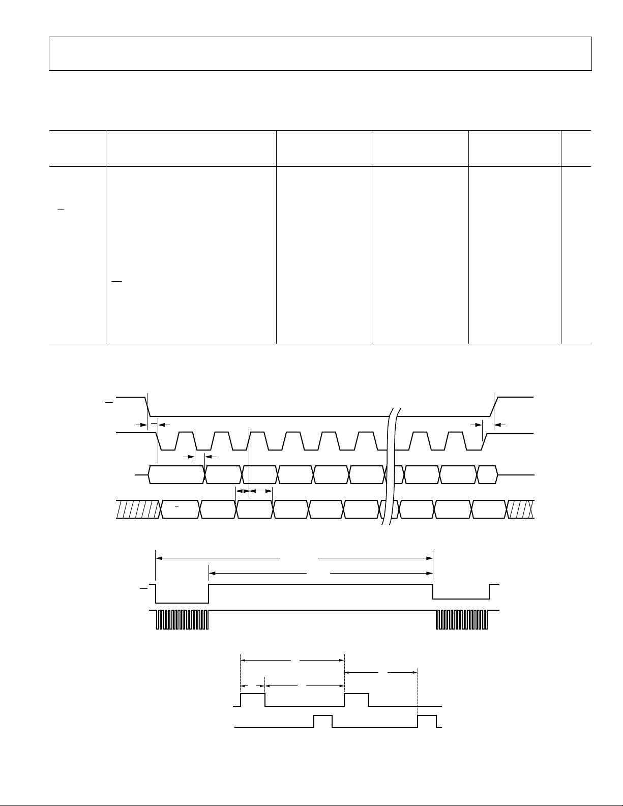
Timing Specifications .................................................................. 5
Timing Diagrams.......................................................................... 5
Absolute Maximum Ratings............................................................ 6
ESD Caution.................................................................................. 6
Pin Configuration and Function Descriptions............................. 7
Typical Performance Characteristics ............................................. 8
Theory of Operation ........................................................................ 9
Basic Operation ............................................................................ 9
Reading Sensor Data.................................................................... 9
Device Configuration .................................................................. 9
Memory Map .............................................................................. 10
Burst Read Data Collection ...................................................... 11
Output Data Registers ............................................................... 11
Calibration................................................................................... 12
Operational Control................................................................... 12
Input/Output Functions............................................................ 14
Diagnostics.................................................................................. 15
Product Identification................................................................ 16
Applications Information.............................................................. 17
Installation/Handling................................................................. 17
Gyroscope Bias Optimization................................................... 17
Input ADC Channel................................................................... 17
Interface Printed Circuit Board (PCB).................................... 17
Outline Dimensions....................................................................... 18
Ordering Guide .......................................................................... 18
REVISION HISTORY
2/11—Rev. 0 to Rev. A
Changes to Gyroscopes Misalignment and Accelerometers
Misalignment Test Conditions/Comments, Table 1 .................... 3
Changes to Table 30 and Table 31 ................................................ 16
1/10—Revision 0: Initial Version
Rev. A | Page 2 of 20

ADIS16367
SPECIFICATIONS
TA = 25°C, VCC = 5.0 V, angular rate = 0°/sec, dynamic range = ±300°/sec ± 1 g, unless otherwise noted.
Table 1.
Parameter Test Conditions/Comments Min Typ Max Unit
GYROSCOPES
Dynamic Range ±1200 ±1400 °/sec
Initial Sensitivity Dynamic range = ±1200°/sec 0.198 0.2 0.202 °/sec/LSB
Dynamic range = ±600°/sec 0.1 °/sec/LSB
Dynamic range = ±300°/sec 0.05 °/sec/LSB
Sensitivity Temperature Coefficient −40°C ≤ TA ≤ +85°C ±40 ppm/°C
Misalignment Axis-to-axis ±0.05 Degrees
Axis-to-frame (package) ±0.5 Degrees
Nonlinearity Best-fit straight line ±0.1 % of FS
Initial Bias Error ±1 σ ±3 °/sec
In-Run Bias Stability 1 σ, SMPL_PRD = 0x0001 0.013 °/sec
Angular Random Walk 1 σ, SMPL_PRD = 0x0001 2.0 °/√hr
Bias Temperature Coefficient −40°C ≤ TA ≤ +85°C ±0.01 °/sec/°C
Linear Acceleration Effect on Bias Any axis, 1 σ (MSC_CTRL[7] = 1) 0.075 °/sec/g
Bias Voltage Sensitivity VCC = 4.75 V to 5.25 V ±0.3 °/sec/V
Output Noise ±1200°/sec range, no filtering 0.8 °/sec rms
Rate Noise Density f = 25 Hz, ±1200°/sec range, no filtering 0.044 °/sec/√Hz rms
3 dB Bandwidth 330 Hz
Sensor Resonant Frequency 14.5 kHz
Self-Test Change in Output Response ±1200°/sec range setting ±170 ±350 ±625 LSB
ACCELEROMETERS Each axis
Dynamic Range ±18
Initial Sensitivity 3.285 3.33 3.38 mg/LSB
Sensitivity Temperature Coefficient −40°C ≤ TA ≤ +85°C ±50 ppm/°C
Misalignment Axis-to-axis 0.2 Degrees
Axis-to-frame (package) ±0.5 Degrees
Nonlinearity Best-fit straight line 0.1 % of FS
Initial Bias Error ±1 σ ±50 mg
In-Run Bias Stability 1 σ 0.2 mg
Velocity Random Walk 1 σ 0.2 m/sec/√hr
Bias Temperature Coefficient −40°C ≤ TA ≤ +85°C ±0.3 mg/°C
Bias Voltage Sensitivity VCC = 4.75 V to 5.25 V 2.5 mg/V
Output Noise No filtering 9 mg rms
Noise Density No filtering 0.5 mg/√Hz rms
3 dB Bandwidth 330 Hz
Sensor Resonant Frequency 5.5 kHz
Self-Test Change in Output Response X-axis and y-axis 59 151 LSB
TEMPERATURE SENSOR
Scale Factor Output = 0x0000 at 25°C (±5°C) 0.136 °C/LSB
ADC INPUT
Resolution 12 Bits
Integral Nonlinearity ±2 LSB
Differential Nonlinearity ±1 LSB
Offset Error ±4 LSB
Gain Error ±2 LSB
Input Range 0 3.3 V
Input Capacitance During acquisition 20 pF
g
Rev. A | Page 3 of 20

ADIS16367
Parameter Test Conditions/Comments Min Typ Max Unit
DAC OUTPUT 5 kΩ/100 pF to GND
Resolution 12 Bits
Relative Accuracy 101 LSB ≤ input code ≤ 4095 LSB ±4 LSB
Differential Nonlinearity ±1 LSB
Offset Error ±5 mV
Gain Error ±0.5 %
Output Range 0 3.3 V
Output Impedance 2 Ω
Output Settling Time 10 μs
LOGIC INPUTS1
Input High Voltage, VIH 2.0 V
Input Low Voltage, VIL 0.8 V
CS Wake-Up Pulse Width
Logic 1 Input Current, IIH V
Logic 0 Input Current, IIL V
All Pins Except RST
RST Pin
signal to wake up from sleep mode
CS
20 μs
= 3.3 V ±0.2 ±10 μA
IH
= 0 V
IL
40 60 μA
1 mA
Input Capacitance, CIN 10 pF
DIGITAL OUTPUTS1
Output High Voltage, VOH I
Output Low Voltage, VOL I
= 1.6 mA 2.4 V
SOURCE
= 1.6 mA 0.4 V
SINK
FLASH MEMORY Endurance2 10,000 Cycles
Data Retention3 T
= 85°C 20 Years
J
FUNCTIONAL TIMES4 Time until data is available
Power-On, Start-Up Time Normal mode, SMPL_PRD ≤ 0x09 180 ms
Low power mode, SMPL_PRD ≥ 0x0A 250 ms
Reset Recovery Time Normal mode, SMPL_PRD ≤ 0x09 60 ms
Low power mode, SMPL_PRD ≥ 0x0A 130 ms
Sleep Mode Recovery Time Normal mode, SMPL_PRD ≤ 0x09 4 ms
Low power mode, SMPL_PRD ≥ 0x0A 9 ms
Flash Memory Test Time Normal mode, SMPL_PRD ≤ 0x09 17 ms
Low power mode, SMPL_PRD ≥ 0x0A 90 ms
Automatic Self-Test Time SMPL_PRD = 0x0001 12 ms
CONVERSION RATE SMPL_PRD = 0x0001 to 0x00FF 0.413 819.2 SPS
Clock Accuracy ±3 %
Sync Input Clock5 0.8 1.2 kHz
POWER SUPPLY Operating voltage range, VCC 4.75 5.0 5.25 V
Power Supply Current Low power mode 24 mA
Normal mode 49 mA
Sleep mode 500 μA
1
The digital I/O signals are driven by an internal 3.3 V supply, and the inputs are 5 V tolerant.
2
Endurance is qualified as per JEDEC Standard 22, Method A117, and measured at −40°C, +25°C, +85°C, and +125°C.
3
The data retention lifetime equivalent is at a junction temperature (TJ) of 85°C as per JEDEC Standard 22, Method A117. Data retention lifetime decreases with junction
temperature.
4
These times do not include thermal settling and internal filter response times (330 Hz bandwidth), which may affect overall accuracy.
5
The sync input clock functions below the specified minimum value, at reduced performance levels.
0.55 V
Rev. A | Page 4 of 20

ADIS16367
TIMING SPECIFICATIONS
TA = 25°C, VCC = 5 V, unless otherwise noted.
Table 2.
Normal Mode
(SMPL_PRD ≤ 0x09)
Parameter Description Min1 Typ Max Mi n1 Typ Max Min1 Typ Max Unit
f
Serial clock 0.01 2.0 0.01 0.3 0.01 1.0 MHz
SCLK
t
Stall period between data 9 75 1/f
STALL
t
Read rate 40 100 μs
READRATE
tCS Chip select to clock edge 48.8 48.8 48.8 ns
t
DOUT valid after SCLK edge 100 100 100 ns
DAV
t
DIN setup time before SCLK rising edge 24.4 24.4 24.4 ns
DSU
t
DIN hold time after SCLK rising edge 48.8 48.8 48.8 ns
DHD
t
, t
SCLKR
SCLK rise/fall times 5 12.5 5 12.5 5 12.5 ns
SCLKF
tDR, tDF DOUT rise/fall times 5 12.5 5 12.5 5 12.5 ns
t
SFS
t
1
high after SCLK edge
CS
Input sync positive pulse width 5 5 μs
5 5 5 ns
tx Input sync low time 100 100 μs
t
2
t
3
1
Guaranteed by design and characterization, but not tested in production.
Input sync to data-ready output 600 600 μs
Input sync period 833 833 μs
Low Power Mode
(SMPL_PRD ≥ 0x0A) Burst Read
μs
SCLK
TIMING DIAGRAMS
CS
SCLK
DOUT
DIN
CS
SCLK
t
CS
1 2 3 4 5 6 15 16
t
DAV
MSB DB14
R/W A5A6 A4 A3 A2
DB13 DB12 DB10DB11 DB2 L SBDB1
t
DSU
t
DHD
D2
Figure 2. SPI Timing and Sequence
t
READRATE
t
STALL
Figure 3. Stall Time and Data Rate
t
3
t
2
t
X
SYNC
CLOCK (DIO 4)
DATA
READY
t
1
Figure 4. Input Clock Timing Diagram
Rev. A | Page 5 of 20
D1 LSB
08398-004
t
SFS
08398-002
08398-003

ADIS16367
ABSOLUTE MAXIMUM RATINGS
Table 3.
Parameter Rating
Acceleration
Any Axis, Unpowered 2000 g
Any Axis, Powered 2000 g
VCC to GND −0.3 V to +6.0 V
Digital Input Voltage to GND −0.3 V to +5.3 V
Digital Output Voltage to GND −0.3 V to VCC + 0.3 V
Analog Input to GND −0.3 V to +3.6 V
Operating Temperature Range −40°C to +105°C
Storage Temperature Range −65°C to +125°C
1
Extended exposure to temperatures outside the specified temperature
range of −40°C to +105°C can adversely affect the accuracy of the factory
calibration. For best accuracy, store the parts within the specified operating
range of −40°C to +105°C.
2
Although the device is capable of withstanding short-term exposure to
150°C, long-term exposure threatens internal mechanical integrity.
1, 2
Stresses above those listed under Absolute Maximum Ratings
may cause permanent damage to the device. This is a stress
rating only; functional operation of the device at these or any
other conditions above those indicated in the operational
section of this specification is not implied. Exposure to absolute
maximum rating conditions for extended periods may affect
device reliability.
Table 4. Package Characteristics
Package Type θJA θ
24-Lead Module (ML-24-2) 39.8°C/W 14.2°C/W 16 grams
ESD CAUTION
Device
JC
Weight
Rev. A | Page 6 of 20
 Loading...