Impact Sensor and Recorder
ADIS16240
Rev. A
Trademarks and registered trade marks are the property of their res pective owners.
Fax: 781.461.3113 ©2009-2011 Analog Devices, Inc. All rights reserved.
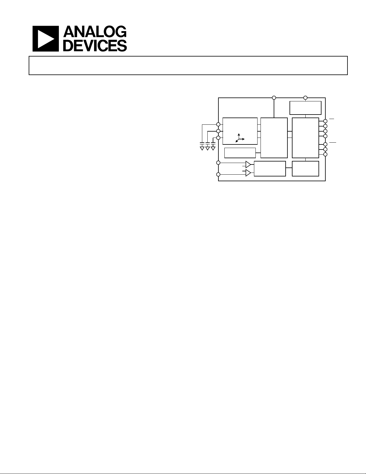
TRIPLE-AXIS
MEMS
ACCELEROMETER
TEMPERATURE
SENSOR
ANALOG-
TO-DIGITAL
CONVERSION
AND
PROCESSING
DIGITAL
CONTROL
AND
SPI
INTERFACE
POWER
MANAGEMENT
EVENT
CAPTURE
BUFFER
ALARM
DETECTION
EVENT TRIGGER
CS
SCLK
DIN
DOUT
DIO2
DIO1
RST
VDDAN
XA
YA
ZA
CMP1
ADIS16240
CMP2
08133-001
Data Sheet
FEATURES
Digital triple-axis accelerometer, ±19 g
Programmable event recorder
Internal and external trigger inputs
Low power operation
Sleep mode current: 100 µA
Continuous sampling current: 1 mA, 1 kSPS
Wake -up and record function
External trigger input and SPI trigger command
Peak acceleration sample-and-hold
Peak XYZ sum-of-squares output
1600 Hz (X, Y) and 550 Hz (Z) sensor bandwidth
Digitally controlled bias correction
Digitally controlled sample rate, up to 4096 SPS
Programmable alarms for condition monitoring
Programmable digital input/output lines
Data-ready output and alarm indicator output
Real-time clock
Digitally activated self-test
Embedded temperature sensor
Programmable power management
SPI-compatible serial interface
Auxiliary 10-bit ADC input
Two analog trigger inputs with programmable threshold
Single-supply operation: 2.4 V to 3.6 V
>4000 g powered shock survivability
APPLICATIONS
Crash or impact detection
Condition monitoring of valuable goods
Safety, shut-off sensing
Impact event recording
Security sensing and tamper detection
Low Power, Programmable
FUNCTIONAL BLOCK DIAGRAM
Figure 1.
GENERAL DESCRIPTION
The ADIS16240 is a fully integrated digital shock detection and
recorder system. It combines industry-leading iMEMS® technology
with a signal processing solution that optimizes dynamic performance for low power applications. The triple-axis sensing element
enables shock measurement in all directions, eliminating the need
for additional sensors and complex mechanical structures for
many applications. The digital serial peripheral interface (SPI)
uses four wires and is compatible with most processor platforms.
The SPI interface provides access to sensor data and a set of configuration registers that control such operational parameters as
offset bias correction, sample rate, sleep mode, peak detection,
and event capture.
Information furnished by Anal og Devices is believed to be accurate and reliable. However, no
responsibility is assumed by Analo g Devices for its use, nor for any infringements of patents or ot her
rights of third parties that may result from its use. Specifications su bject to change without notice. No
license is granted by implication or ot herwise under any patent or patent rights of An alog Devices.
The programmable event recorder offers two trigger modes. The
internal mode monitors continuous sampled data and triggers the
capture, based on the user-defined threshold. The external mode
uses the two comparator inputs and a user-defined threshold to
trigger the event captures. This function also provides user configuration controls for capture length, pretrigger data, and data storage.
Each event is stored with a header that captures temperature, power
supply, and time. Several power management features, including
sleep mode and a wake-up function, enable power optimization
with respect to specific mechanical system requirements.
The ADIS16240 is available in a 12 mm × 12 mm laminate-based
ball grid array (BGA) that meets IPC/JEDEC standards for Pb-free
solder reflow processing (J-STD-020C and J-STD-033).
One Technology Way, P.O. Box 9106, Norwood, MA 02062-9106, U.S.A.
Tel: 781.329.4700 www.analog.com

ADIS16240 Data Sheet
TABLE OF CONTENTS
Features .............................................................................................. 1
Applications ....................................................................................... 1
Functional Block Diagram .............................................................. 1
General Description ......................................................................... 1
Revision History ............................................................................... 2
Specifications ..................................................................................... 3
Timing Specifications .................................................................. 4
Absolute Maximum Ratings ............................................................ 5
ESD Caution .................................................................................. 5
Pin Configuration and Function Descriptions ............................. 6
Typical Performance Characteristics ............................................. 7
Theory of Operation ........................................................................ 8
Sensing Element ........................................................................... 8
Data Sampling and Processing ................................................... 8
REVISION HISTORY
10/11—Rev. 0 to Rev. A
Added Applications Information Section, Figure 23, Figure 24,
Figure 25, Renumbered Sequentially ........................................... 16
Updated Outline Dimensions ....................................................... 18
Changes to Ordering Guide .......................................................... 18
4/09—Revision 0: Initial Version
User Interface .................................................................................8
Capture ...........................................................................................8
Basic Operation .................................................................................9
Memory Map .............................................................................. 10
Output Data Registers ............................................................... 11
Event Recorder ........................................................................... 12
Operational Control ................................................................... 14
Applications Information .............................................................. 16
Assembly ...................................................................................... 16
Interface Printed Circuit Board (PCB) .................................... 16
Outline Dimensions ....................................................................... 17
Ordering Guide .......................................................................... 17
Rev. A | Page 2 of 20

Data Sheet ADIS16240
Nonlinearity
Compare with best fit line
±2 % FS
No external capacitance
Z 550 Hz
Sleep Mode Current
100 µA
SPECIFICATIONS
TA = 25°C, VDD = 2.4 V to 3.6 V unless otherwise noted.
Table 1.
Parameter Conditions Axis Min Typ Max Unit
ACCELEROMETER
Dynamic Range ±16 ±19
Initial Sensitivity 51.4 mg/LSB
Sensitivity Temperature Coefficient −40°C to +85°C ±0.01 %
Sensitivity Change with Supply Voltage 2.4 V < VDD < 3.6 V X, Y 6 %
Sensor-to-Sensor Alignment Error ±0.1 Degrees
Cross-Axis Sensitivity ±1 %
Initial Bias Error −2.7 +2.7
Bias Temperature Coefficient ±1 mg/°C
Bias Voltage Sensitivity TBD mg/V
Output Noise 24 mg rms
Noise Density 480
Bandwidth No external capacitance X, Y 1600 Hz
Sensor Resonant Frequency 5.5 kHz
Self-Test Change in Output Response X −10 −21 −39 LSB
Y +10 +21 +39 LSB
Z +10 +36 +65 LSB
TEMPERATURE SENSOR SCALE FACTOR TEMP_OUT = 0x0133 (307) at 25°C 0.244 °C/LSB
ADC INPUT
Input Range 0 VDD V
Resolution 10 Bits
Integral Nonlinearity, INL ±1 ±2 LSB
Differential Nonlinearity, DNL ±1 ±1.25 LSB
Offset Error ±1 ±2 LSB
Gain Error ±1 ±3 LSB
Input Capacitance 11 pF
LOGIC INPUTS1
Input High Voltage, V
Input Low Voltage, V
Logic 1 Input Current, I
Logic 0 Input Current, I
2.0 V
INH
0.8 V
INL
VIH = VDD ±0.2 ±1 µA
INH
VIL = 0 V −40 −60 μA
INL
Input Capacitance, CIN 10 pF
DIGITAL OUTPUTS
Output High Voltage, VOH I
Output Low Voltage, VOL I
= 1.6 mA 2.4 V
SOURCE
= 1.6 mA 0.4 V
SINK
START-UP TIME
Initial, Reset Recovery 32 ms
FLASH MEMORY
Endurance2 10,000 Cycles
Data Retention3 TJ = 85°C 20 Years
CONVERSION RATE SETTING 4096 SPS
POWER SUPPLY 2.4 3.6 V
Average Supply Current4 SMPL_PRD = 0x1F, VDD = 2.5 V 1 mA
g
g
µg/√Hz
1
Note that the inputs are 5 V tolerant.
2
Endurance is qualified as per JEDEC Standard 22, Method A117 and measured at −40°C, +25°C, +85°C, and +105°C.
3
Retention lifetime equivalent at junction temperature (TJ) of 55°C as per JEDEC Standard 22, Method A117. Retention lifetime decreases with junction temperature.
4
Instantaneous current has periodic peaks at the sample rate that can reach 30 mA.
Rev. A | Page 3 of 20

ADIS16240 Data Sheet
t
Data input hold time after SCLK rising edge
20
ns
CS
SCLK
t
DATARATE
08133-002
CS
SCLK
DOUT
DIN
1 2 3 4 5 6 15 16
W/R A5A6 A4 A3 A2
D2
MSB
DB14
D1 LSB
DB13 DB12 DB10DB11 DB2 LSBDB1
t
CS
t
SFS
t
DAV
t
DHD
t
DSU
08133-003
TIMING SPECIFICATIONS
TA = 25°C, VDD = 3.3 V, unless otherwise noted.
Table 2.
Parameter Description Min1 Typ Max1 Unit
f
Serial clock rate2 0.01 2.5 MHz
SCLK
t
Chip select period
DATA RATE
tCS Chip select to clock edge 120 ns
t
Data output valid after SCLK edge 30 ns
DAV
t
Data input setup time before SCLK rising edge 20 ns
DSU
DHD
tDF Data output fall time 10 25 ns
tDR Data output rise time 10 25 ns
t
SFS
1
Guaranteed by design; typical specifications are not tested or guaranteed.
2
Based on sample rate selection.
CS high after SCLK edge
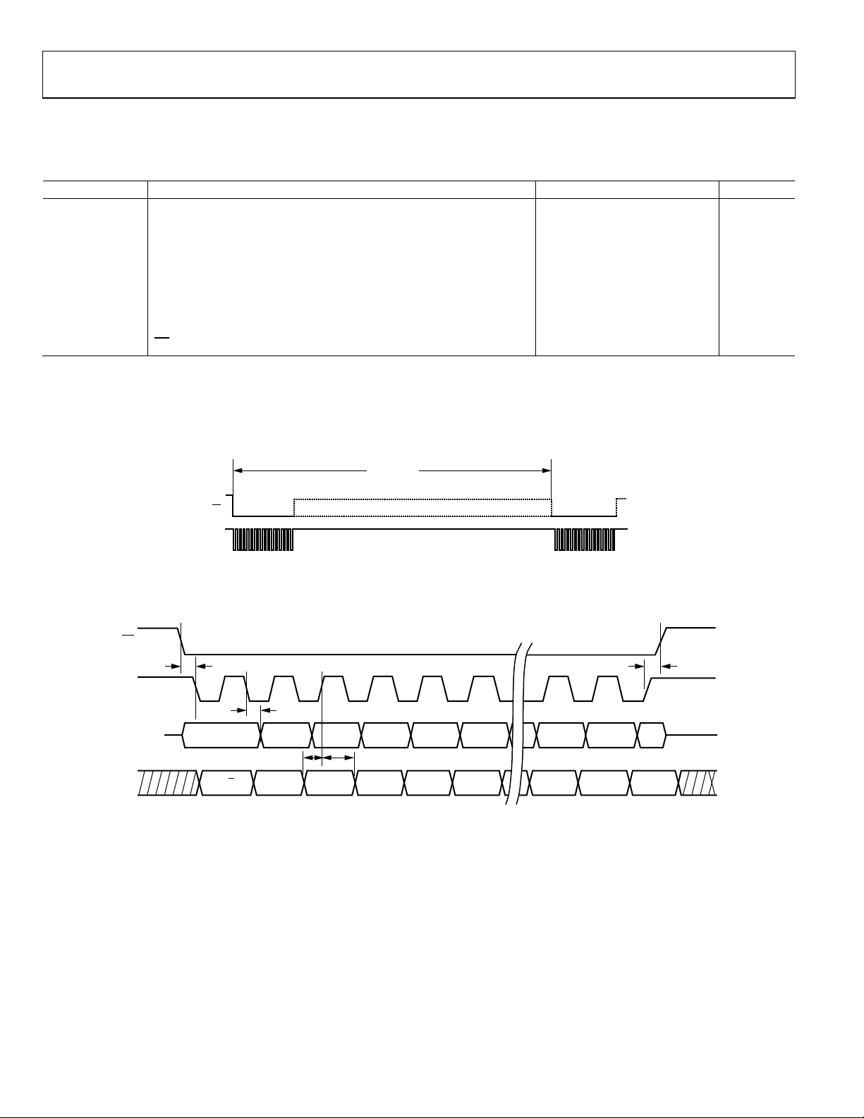
Timing Diagrams
2
60 μs
430 ns
Figure 2. SPI Chip Select Timing
Figure 3. SPI Timing (Utilizing SPI Settings Typically Identified as Phase = 1, Polarity = 1)
Rev. A | Page 4 of 20

Data Sheet ADIS16240
Parameter
Rating
Storage Temperature Range
−65°C to +150°C
ABSOLUTE MAXIMUM RATINGS
Table 3.
Acceleration
Any Axis, Unpowered 2000 g
Any Axis, Powered 2000 g
VDD to GND −0.3 V to +3.6 V
Digital Input Voltage to GND −0.3 V to VDD + 0.3 V
Analog Inputs to GND −0.3 V to VDD + 0.3 V
Operating Temperature Range −40°C to +85°C
Stresses above those listed under Absolute Maximum Ratings
may cause permanent damage to the device. This is a stress
rating only; functional operation of the device at these or any
other conditions above those indicated in the operational
section of this specification is not implied. Exposure to absolute
maximum rating conditions for extended periods may affect
device reliability.
ESD CAUTION
Rev. A | Page 5 of 20

ADIS16240 Data Sheet
08133-004
21 4
5
6
9
10
11
3
7
8
A
B
TOP VIEW
NOTES
1. THE ACTUAL PI NS ARE NOT
VISIBLE FROM T HE TO P VIEW.
C
D
E
F
G
J
H
K
L
A
Z
A1
A
Y
A
X
A
Z
A
Y
A
X
08133-005
X
E10, E11
SCLK
I
SPI Serial Clock
K8, L8
AN I Analog Input Channel
H1, H2
YA O Y-Axis Accelerometer Filter Pin
NC No Connect
PIN CONFIGURATION AND FUNCTION DESCRIPTIONS
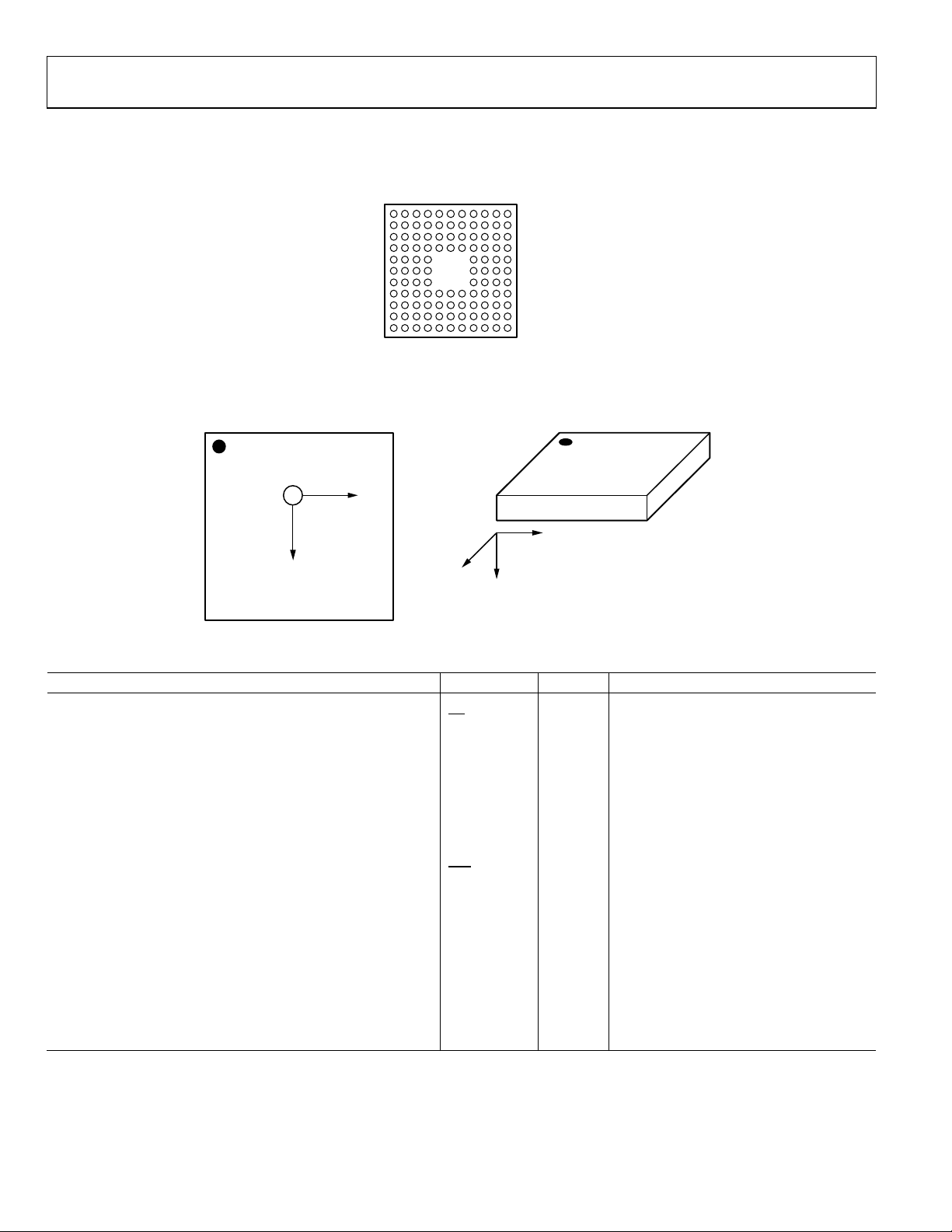
Figure 4. Pin Configuration (Top View)
Figure 5. Axis Orientation of Device (Top View)
Table 4. Pin Function Descriptions
Pin No. Mnemonic Type1 Description
F10, F11
CS
I SPI Chip Select, Active Low
G10, G11 DIN I SPI Data Input
H10, H11 DOUT O SPI Data Output
J10, J11 DIO2 I/O Multifunction Digital Input/Output 2
K9, L9 DIO1 I/O Multifunction Digital Input/Output 1
K7, L7 CMP2 I Analog Comparator Input 2
K6, L6 CMP1 I Analog Comparator Input 1
K3, L3
J1, J2 XA O X-Axis Accelerometer Filter Pin
G1, G2 ZA O Z-Axis Accelerometer Filter Pin
A5, B5 ST I Self-Test Input Control Line
D4 to D8, E4, E8, F4, F8, G4, G8, H4 to H8 VDD S Power Supply, 3.3 V
A1, A2, A10, A11, B1, B2, B10, B11, C3 to C9, D3, D9, E3, E9, F3, F9,
G3, G9, H3, H9, J3 to J9, K1, K2, K10, K11, L1, L2, L10, L11
A3, A4, A6 to A9, B3, B4, B6 to B9, C1, C2, C10, C11, D1, D2, D10,
D11, E1, E2, F1, F2, K4, K5, L4, L5
1
I = input, O = output, I/O = input/output, S = supply.
RST
I Reset, Active Low, No Pull-Up Resistor
GND S Ground
Rev. A | Page 6 of 20
 Loading...