

with FFT Analysis and Storage
ADIS16228
Rev. B
Information furnished by Analog Devices is believed to be accurate and reliable. However, no
Trademarks and registered trademarks are the property of their respective owners.
Fax: 781.461.3113 ©2011–2012 Analog Devices, Inc. All rights reserved.
ADIS16228
RECORD
STORAGE
ALARMS
INPUT/
OUTPUT
CONTROLLER
ADC
TRIAXIAL
MEMS
SENSOR
TEMP
SENSOR
SUPPLY
POWER
MANAGEMENT
CS
SCLK
DIN
DOUT
GND
VDDRSTDIO1
CONTROL
REGISTERS
SPI
PORT
OUTPUT
REGISTERS
FILTER
WINDOW
FFT
CAPTURE
BUFFER
10069-001
DIO2
Data Sheet
FEATURES
Frequency domain triaxial vibration sensor
Flat frequency response up to 5 kHz
Digital acceleration data, ±18 g measurement range
Digital range settings: 0 g to 1 g/5 g/10 g/20 g
Real-time sample mode: 20.48 kSPS, single-axis
Capture sample modes: 20.48 kSPS, three axes
Trigger modes: SPI, timer, external
Programmable decimation filter, 11 rate settings
Multirecord capture for selected filter settings
Manual capture mode for time domain data collection
FFT, 512-point, real valued, all three axes (x, y, z)
3 windowing options: rectangular, Hanning, flat top
Programmable FFT averaging: up to 255 averages
Storage: 14 FFT records on all three axes (x, y, z)
Programmable alarms, 6 spectral bands
2-level settings for warning and fault definition
Adjustable response delay to reduce false alarms
Internal self-test with status flags
Digital temperature and power supply measurements
2 auxiliary digital I/Os
SPI-compatible serial interface
Identification registers: serial number, device ID, user ID
Single-supply operation: 3.0 V to 3.6 V
Operating temperature range: −40°C to +125°C
15 mm × 24 mm × 15 mm aluminum package, flex connector
APPLICATIONS
Vibration analysis
Condition monitoring
Machine health
Instrumentation, diagnostics
Safety shutoff sensing
Digital Triaxial Vibration Sensor
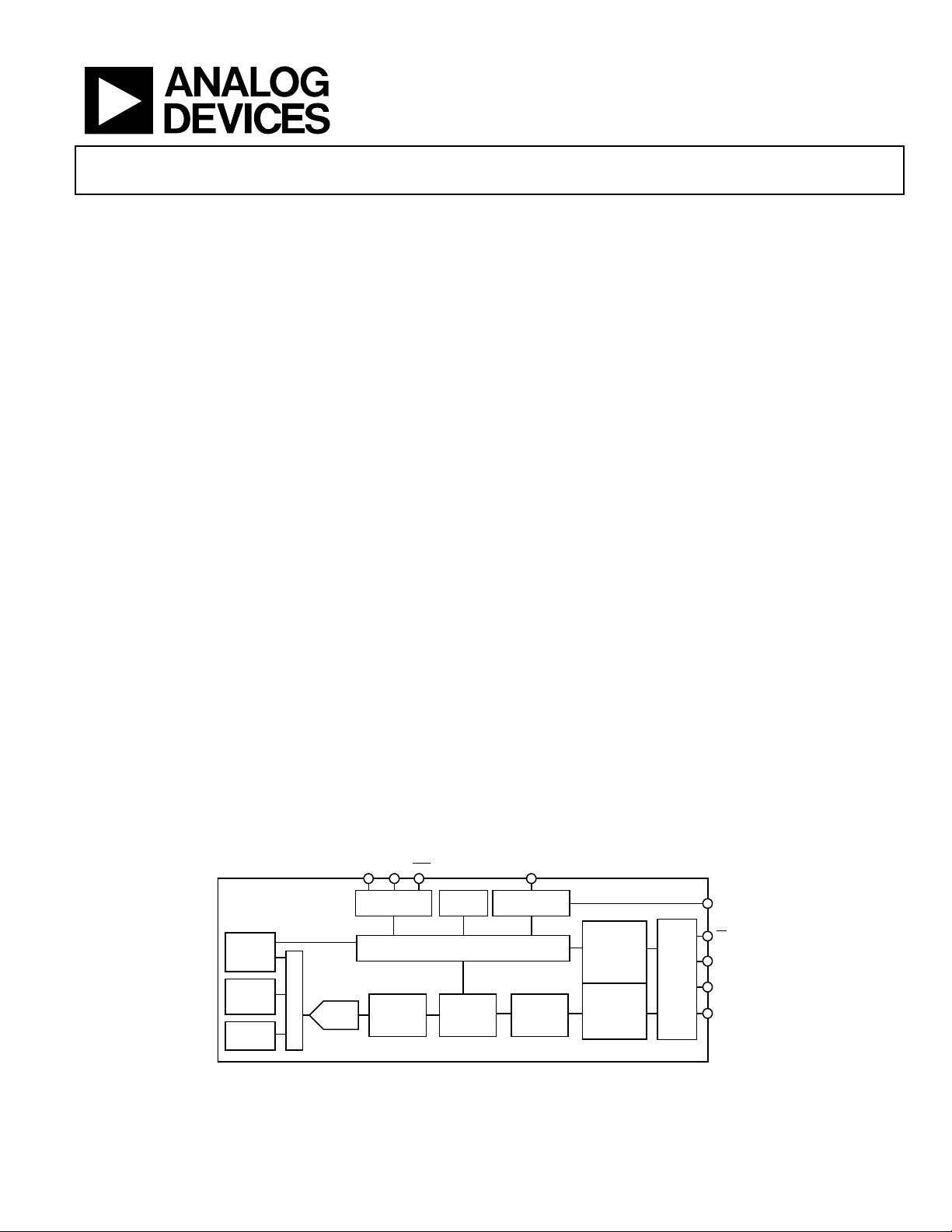
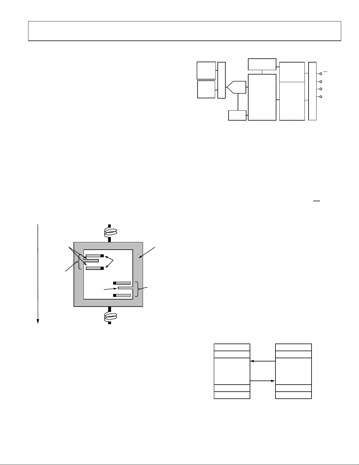
GENERAL DESCRIPTION
The ADIS16228 iSensor® is a complete vibration sensing system
that combines triaxial acceleration sensing with advanced time
domain and frequency domain signal processing. Time domain
signal processing includes a programmable decimation filter
and selectable windowing function. Frequency domain processing
includes a 512-point, real-valued FFT for each axis, along with
FFT averaging, which reduces the noise floor variation for finer
resolution. The 14-record FFT storage system offers users the
ability to track changes over time and capture FFTs with multiple
decimation filter settings.
The 20.48 kSPS sample rate and 5 kHz flat frequency band
provide a frequency response that is suitable for many machine
health applications. The aluminum core provides excellent
mechanical coupling to the MEMS acceleration sensors. An
internal clock drives the data sampling and signal processing
system during all operations, which eliminates the need for an
external clock source. The data capture function has three modes
that offer several options to meet the needs of many different
applications. In addition, real-time mode provides direct access
to streaming data on one axis. The SPI and data buffer structure
provide convenient access to data output. The ADIS16228 also
offers a digital temperature sensor and digital power supply
measurements.
The ADIS16228 is available in a 15 mm × 24 mm × 15 mm module
with flanges, machine screw holes (M2 or 2-56), and a flexible
connector that enables simple user interface and installation. It
has an extended operating temperature range of −40°C to +125°C.
FUNCTIONAL BLOCK DIAGRAM
responsibility is assumed by Analog Devices for its use, nor for any infringements of patents or other
rights of third parties that may result from its use. Spe cifications subject to change without n otice. No
license is granted by implication or otherwise under any patent or patent rights of Analog Devices.
Figure 1.
One Technology Way, P.O. Box 9106, Norwood, MA 02062-9106, U.S.A.
Tel: 781.329.4700
www.analog.com

ADIS16228 Data Sheet
TABLE OF CONTENTS
Features .............................................................................................. 1
Applications ....................................................................................... 1
General Description ......................................................................... 1
Functional Block Diagram .............................................................. 1
Revision History ............................................................................... 2
Specifications ..................................................................................... 3
Timing Specifications .................................................................. 4
Absolute Maximum Ratings ............................................................ 5
ESD Caution .................................................................................. 5
Pin Configuration and Function Descriptions ............................. 6
Theory of Operation ........................................................................ 7
Sensing Element ........................................................................... 7
Signal Processing .......................................................................... 7
User Interface ................................................................................ 7
Basic Operation................................................................................. 8
SPI Write Commands .................................................................. 8
SPI Read Commands ................................................................... 8
Data Recording and Signal Processing ........................................ 11
Recording Mode ......................................................................... 11
Spectral Record Production ...................................................... 12
Sample Rate/Filtering ................................................................. 12
Dynamic Range/Sensitivity ....................................................... 14
Pre-FFT Windowing .................................................................. 15
FFT ............................................................................................... 16
Recording Times ......................................................................... 16
Data Records ............................................................................... 16
FFT Record Flash Endurance ................................................... 16
Spectral Alarms ............................................................................... 17
Alarm Definition ........................................................................ 17
Alarm Indicator Signals ............................................................. 18
Alarm Flags and Conditions ..................................................... 18
Alarm Status ................................................................................ 19
Worst -Case Condition Monitoring.......................................... 19
Reading Output Data ..................................................................... 20
Reading Data from the Data Buffer ......................................... 20
Accessing FFT Record Data ...................................................... 20
Data Format ................................................................................ 21
Real-Time Data Collection ....................................................... 21
Power Supply/Temperature ....................................................... 21
FFT Event Header ...................................................................... 22
System Tools .................................................................................... 23
Global Commands ..................................................................... 23
Status/Error Flags ....................................................................... 23
Power-Down ............................................................................... 23
Operation Managment .............................................................. 24
Input/Output Functions ............................................................ 24
Self-Tes t ....................................................................................... 25
Flash Memory Management ..................................................... 25
Device Identification .................................................................. 25
Applications Information .............................................................. 26
Interface Board ........................................................................... 26
Mating Connector ...................................................................... 26
Outline Dimensions ....................................................................... 27
Ordering Guide .......................................................................... 27
REVISION HISTORY
3/12—Rev. A to Rev. B
Changes to Recording Times Section and Table 21 ................... 16
Changes to Interface Board Section ............................................. 26
8/11—Rev. 0 to Rev. A
Changes to General Description .................................................... 1
Changes to Output Noise and Bandwidth Parameters, Table 1 .... 3
Added CAL_ENABLE Register to Table 8 .................................. 10
Changes to Real-Time Mode Section; Changes to Table 11;
Change to Figure 14 ....................................................................... 12
Changes to Figure 15 ...................................................................... 13
Added Dynamic Range/Sensitivity Section; Added Table 13,
Renumbered Sequentially; Added Figure 16, Figure 17, and
Figure 18, Renumbered Sequentially ........................................... 14
Rev. B | Page 2 of 28
Change to Dynamic Range Settings Section............................... 15
Changes to Recording Times Section .......................................... 16
Changes to Figure 20 and Figure 21 ............................................ 20
Changes to Table 49, Table 50, and Table 51; Change to
Real-Time Data Collection Section ............................................. 21
Change to Power-Down Section .................................................. 23
7/11—Revision 0: Initial Version

Data Sheet ADIS16228
Bandwidth
±5% flatness,2 CAL_ENABLE[4] = 0, see Figure 17
840 Hz
FLASH MEMORY
SPECIFICATIONS
TA = −40°C to +125°C, VDD = 3.3 V, unless otherwise noted.
Table 1.
Parameter Test Conditions/Comments Min Typ Max Unit
ACCELEROMETERS
Measurement Range1 TA = 25°C ±18
Sensitivity, FFT TA = 25°C, 0 g to 20 g range setting 0.3052 mg/LSB
Sensitivity, Time Domain TA = 25°C 0.6104 mg/LSB
Sensitivity Error TA = 25°C ±6 %
Nonlinearity With respect to full scale ±0.2 ±1.25 %
Cross-Axis Sensitivity 2.6 %
Alignment Error With respect to package 1.5 Degrees
Offset Error TA = 25°C ±1
Offset Temperature Coefficient 1 mg/°C
Output Noise TA = 25°C, 20.48 kHz sample rate, time domain 12 mg rms
Output Noise Density TA = 25°C, 10 Hz to 1 kHz 0.248 mg/√Hz
±5% flatness,2 CAL_ENABLE[4] = 1, see Figure 18 5000 Hz
Sensor Resonant Frequency 5.5 kHz
LOGIC INPUTS3
Input High Voltage, V
Input Low Voltage, V
Logic 1 Input Current, I
Logic 0 Input Current, I
All Except
RST
RST
−1 mA
2.0 V
INH
0.8 V
INL
VIH = 3.3 V ±0.2 ±1 µA
INH
VIL = 0 V
INL
−40 −60 µA
Input Capacitance, CIN 10 pF
DIGITAL OUTPUTS3
Output High Voltage, VOH I
Output Low Voltage, VOL I
= 1.6 mA 2.4 V
SOURCE
= 1.6 mA 0.4 V
SINK
g
g
Endurance4 10,000 Cycles
Data Retention5 TJ = 85°C, see Figure 23 20 Years
START-UP TIME6
Initial Startup 202 ms
Reset Recovery7
pulse low or GLOB_CMD[7] = 1 54 ms
RST
Sleep Mode Recovery 2.3 ms
CONVERSION RATE REC_CTRL1[11:8] = 0x1 (SR0 sample rate selection) 20.48 kSPS
Clock Accuracy 3 %
POWER SUPPLY Operating voltage range, VDD 3.0 3.3 3.6 V
Power Supply Current Record mode, TA = 25°C 40 48 mA
Sleep mode, TA = 25°C 230 µA
1
The maximum range depends on the frequency of vibration.
2
Assumes that frequency flatness calibration is enabled.
3
The digital I/O signals are 5 V tolerant.
4
Endurance is qualified as per JEDEC Standard 22, Method A117 and measured at −40°C, +25°C, +85°C, and +125°C.
5
Retention lifetime equivalent at junction temperature (TJ) = 85°C as per JEDEC Standard 22, Method A117. Retention lifetime depends on junction temperature.
6
The start-up times presented reflect the time it takes for data collection to begin.
7
RST
The
pin must be held low for at least 15 ns.
Rev. B | Page 3 of 28
ADIS16228 Data Sheet
CS
SCLK
DOUT
DIN
1 2 3 4 5 6 15 16
R/W A5A6 A4 A3 A2
D2
MSB DB14
D1 LSB
DB13 DB12 DB10DB11 DB2 LSBDB1
t
CS
t
SFS
t
DAV
t
SR
t
SF
t
DHD
t
DSU
10069-002
CS
SCLK
t
STALL
10069-003
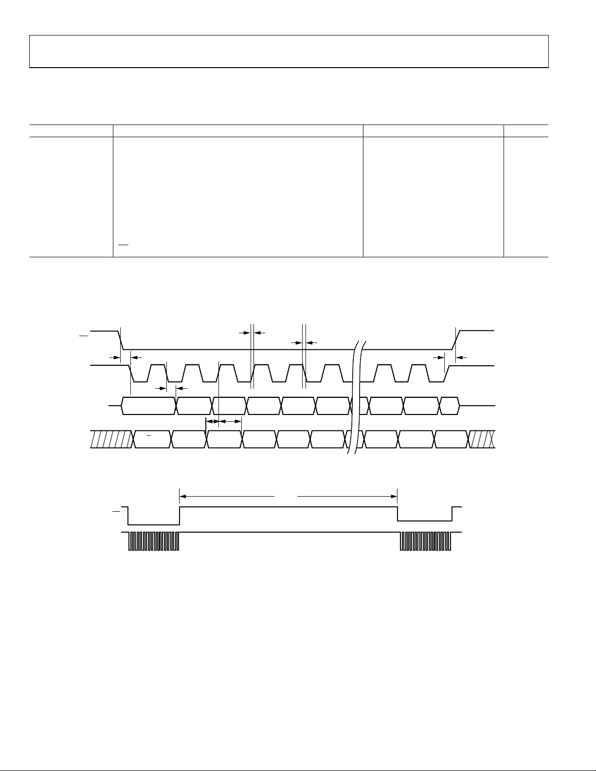
TIMING SPECIFICATIONS
TA = 25°C, VDD = 3.3 V, unless otherwise noted.
Table 2.
Parameter Description Min1 Typ Max Unit
f
SCLK frequency 0.01 2.5 MHz
SCLK
t
Stall period between data, between 16th and 17th SCLK 16.5 µs
STAL L
tCS Chip select to SCLK edge 48.8 ns
t
DOUT valid after SCLK edge 100 ns
DAV
t
DIN setup time before SCLK rising edge 24.4 ns
DSU
t
DIN hold time after SCLK rising edge 48.8 ns
DHD
tSR SCLK rise time 12.5 ns
tSF SCLK fall time 12.5 ns
tDF, tDR DOUT rise/fall times 5 12.5 ns
t
SFS
1
Guaranteed by design, not tested.
Timing Diagrams
high after SCLK edge 5 ns
CS
Figure 2. SPI Timing and Sequence
Figure 3. DIN Bit Sequence
Rev. B | Page 4 of 28
Data Sheet ADIS16228
Any Axis, Unpowered
2000 g
ABSOLUTE MAXIMUM RATINGS
Table 3.
Parameter Rating
Acceleration
Any Axis, Powered 2000 g
VDD to GND −0.3 V to +6.0 V
Digital Input Voltage to GND −0.3 V to +5.3 V
Digital Output Voltage to GND −0.3 V to +3.6 V
Analog Inputs to GND −0.3 V to +3.6 V
Temperature
Operating Temperature Range −40°C to +125°C
Storage Temperature Range −65°C to +150°C
Stresses above those listed under Absolute Maximum Ratings
may cause permanent damage to the device. This is a stress
rating only; functional operation of the device at these or any
other conditions above those indicated in the operational
section of this specification is not implied. Exposure to absolute
maximum rating conditions for extended periods may affect
device reliability.
Table 4. Package Characteristics
Package Type θJA θJC Device Weight
15-Lead Module 31°C/W 11°C/W 6.5 grams
ESD CAUTION
Rev. B | Page 5 of 28
ADIS16228 Data Sheet
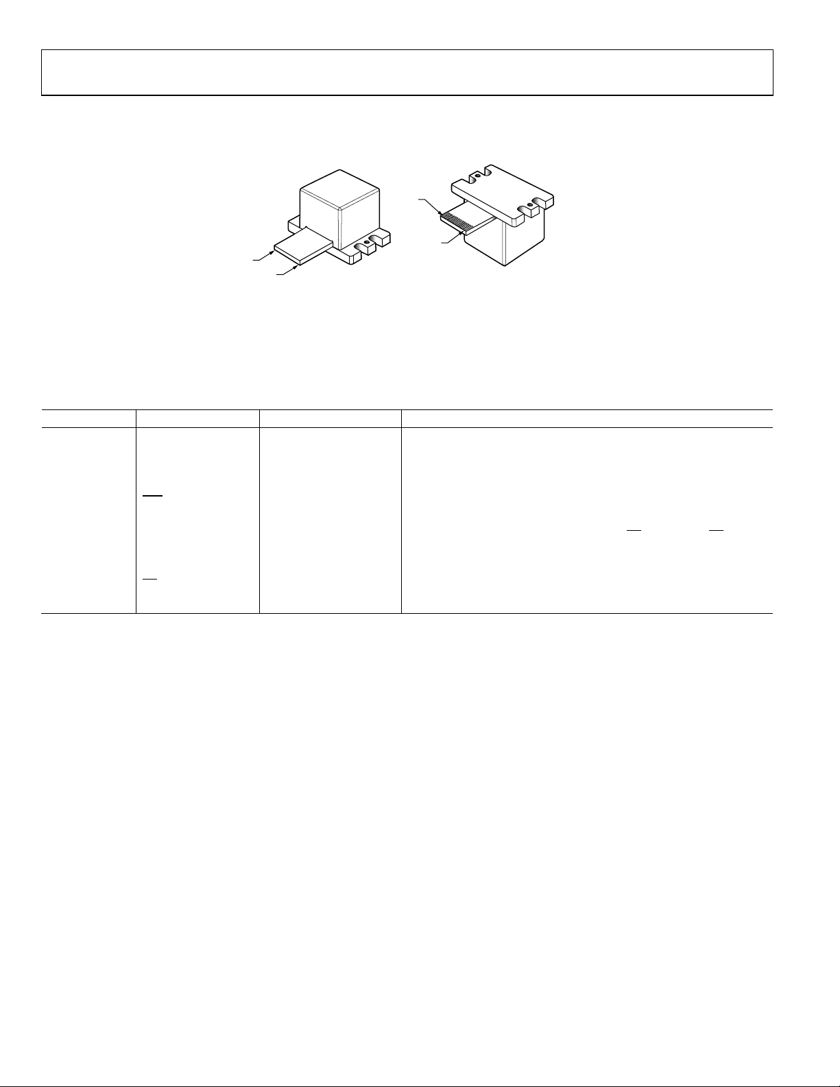
10069-004
TOP VIEW
BOTTOM VIEW
PIN 15
PIN 15
PIN 1
PIN 1
NOTES
1. LEADS ARE E X P OSED COPPER P ADS THAT ARE LOCATED ON
THE BOTTOM SIDE OF THE FLEXIBLE INTERFACE CABLE.
2. PACKAGE IS NOT SUITABLE FOR SOLDER REFLOW ASSEMBLY PROCESSES.
3. EXAMPLE MATING CONNECTOR:AVX CORPORATION
FLAT FLEXIBLE CONNECTOR (FFC)
P/N: 04-6288-015-000- 846.
3, 4, 5, 8
GND S Ground.
PIN CONFIGURATION AND FUNCTION DESCRIPTIONS
Figure 4. Pin Configuration
Table 5. Pin Function Descriptions
Pin No. Mnemonic Type1 Description
1, 2 VDD S Power Supply, 3.3 V.
6, 9 DNC N/A No Connect. Do not connect to these pins.
7 DIO2 I/O Digital Input/Output Line 2.
10
I Reset, Active Low.
RST
11 DIN I SPI, Data Input.
12 DOUT O SPI, Data Output. DOUT is an output when CS is low. When CS is high,
DOUT is in a three-state, high impedance mode.
13 SCLK I SPI, Serial Clock.
14
I SPI, Chip Select.
CS
15 DIO1 I/O Digital Input/Output Line 1.
1
S is supply, O is output, I is input, and I/O is input/output.
Rev. B | Page 6 of 28
Data Sheet ADIS16228
MOVABLE
FRAME
ACCELERATION
UNIT
FORCING
CELL
UNIT SENSING
CELL
MOVING
PLATE
FIXED
PLATES
PLATE
CAPACITORS
ANCHOR
ANCHOR
10069-005
TRIAXIAL
MEMS
SENSOR
CLOCK
CONTROLLER
CAPTURE
BUFFER
CONTROL
REGISTERS
SPI
SIGNALS
SPI PORT
OUTPUT
REGISTERS
TEMP
SENSOR
ADC
10069-006
CS
SCLK
DIN
DOUT
NONVOLATILE
FLASH MEMORY
(NO SPI ACCESS)
MANUAL
FLASH
BACKUP
START-UP
RESET
VOLATILE
SRAM
SPI ACCESS
10069-007
THEORY OF OPERATION
The ADIS16228 is a vibration sensing system that combines a
triaxial MEMS accelerometer with advanced signal processing.
The SPI-compatible port and user register structure provide
convenient access to frequency domain vibration data and many
user controls.
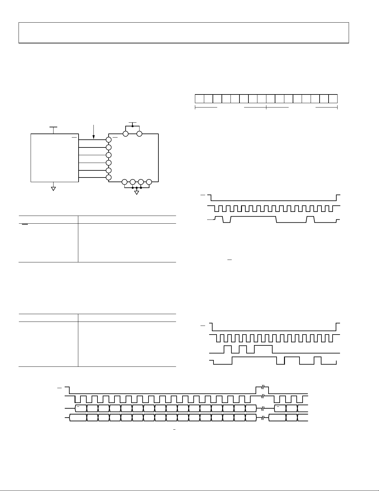
SENSING ELEMENT
Digital vibration sensing in the ADIS16228 starts with a MEMS
accelerometer core on each axis. Accelerometers translate linear
changes in velocity into a representative electrical signal, using
a micromechanical system like the one shown in Figure 5. The
mechanical part of this system includes two different frames
(one fixed, one moving) that have a series of plates to form
a variable, differential capacitive network. When experiencing
the force associated with gravity or acceleration, the moving
frame changes its physical position with respect to the fixed
frame, which results in a change in capacitance. Tiny springs
tether the moving frame to the fixed frame and govern the
relationship between acceleration and physical displacement.
A modulation signal on the moving plate feeds through each
capacitive path into the fixed frame plates and into a demodulation
circuit, which produces the electrical signal that is proportional
to the acceleration acting on the device.
SIGNAL PROCESSING
Figure 6 offers a simplified block diagram for the ADIS16228.
The signal processing stage includes time domain data capture,
digital decimation/filtering, windowing, FFT analysis, FFT
averaging, and record storage. See Figure 14 for more details
on the signal processing operation.
Figure 5. MEMS Sensor Diagram
Figure 6. Simplified Sensor Signal Processing Block Diagram
USER INTERFACE
SPI Interface
The user registers (which include both the output registers and
the control registers, as shown in Figure 6) manage user access
to both sensor data and configuration inputs. Each 16-bit register
has its own unique bit assignment and two addresses: one for its
upper byte and one for its lower byte. Table 8 provides a memory
map for each register, along with its function and lower byte
address. The data collection and configuration command uses
the SPI, which consists of four wires. The chip select (
activates the SPI interface, and the serial clock (SCLK)
synchronizes the serial data lines. Input commands clock into
the DIN pin, one bit at a time, on the SCLK rising edge. Output
data clocks out of the DOUT pin on the SCLK falling edge.
When the SPI is used as a slave device, the DOUT contents
reflect the information requested using a DIN command.
Dual-Memory Structure
The user registers provide addressing for all input/output operations
in the SPI interface. The control registers use a dual-memory
structure. The controller uses SRAM registers for normal
operation, including user-configuration commands. The flash
memory provides nonvolatile storage for control registers that
have flash backup (see Table 8). Storing configuration data
in the flash memory requires a manual flash update command
(GLOB_CMD[6] = 1, DIN = 0xBE40). When the device powers
on or resets, the flash memory contents load into the SRAM, and
the device starts producing data according to the configuration
in the control registers.
CS
) signal
Rev. B | Page 7 of 28
Figure 7. SRAM and Flash Memory Diagram
ADIS16228 Data Sheet
SYSTEM
PROCESSOR
SPI MASTER
ADIS16228
SCLK
CS
DIN
DOUT
SCLK
SS
MOSI
MISO
3.3V
IRQ2
IRQ1
DIO2
VDD
I/O LINES ARE COMPATIBLE WITH
3.3V OR 5V LOGIC LEVELS
14
13
11
12
7
DIO1
15
1 2
3 4 5 8
10069-008
UPPER BYTE
15 14 13 12 11 10 9 8 7 6 5 4 3 2 1 0
LOWER BYTE
10069-009
CS
DIN
SCLK
10069-010
DOUT = 0011 1111 0110 0100 = 0x3F64 = 16,228 = P ROD_ID
SCLK
CS
DIN
DOUT
10069-011
R/W
R/W
A6 A5 A4 A3 A2 A1 A0 D7 D6 D5 D4 D3 D2 D1 D0
DB0DB1DB2DB3DB4DB5DB6DB7DB8DB9DB10DB11DB12DB13DB14DB15
NOTES
1. DOUT BITS ARE BASED ON THE PREVIOUS 16-BIT SEQUENCE (R/W = 0).
CS
SCLK
DIN
DOUT
A6 A5
DB13DB14
DB15
10069-012
BASIC OPERATION
The ADIS16228 uses a SPI for communication, which enables
a simple connection with a compatible, embedded processor
platform, as shown in Figure 8. The factory default configuration
for DIO1 provides a busy indicator signal that transitions low
when an event completes and data is available for user access.
Use the DIO_CTRL register (see Table 66) to reconfigure DIO1
and DIO2, if necessary.
Figure 8. Electrical Hook-Up Diagram
Table 6. Generic Master Processor Pin Names and Functions
Pin Name Function
Slave select
SS
SCLK Serial clock
MOSI Master output, slave input
MISO Master input, slave output
IRQ1, IRQ2 Interrupt request inputs (optional)
The ADIS16228 SPI interface supports full duplex serial
communication (simultaneous transmit and receive) and uses
the bit sequence shown in Figure 12. Tab l e 7 provides a list of
the most common settings that require attention to initialize
a processor serial port for the ADIS16228 SPI interface.
Table 7. Generic Master Processor SPI Settings
Processor Setting Description
Master The ADIS16228 operates as a slave.
SCLK Rate ≤ 2.5 MHz Bit rate setting.
SPI Mode 3 Clock polarity/phase
(CPOL = 1, CPHA = 1).
MSB First Bit sequence.
16-Bit Shift register/data length.
Tabl e 8 provides a list of user registers with their lower byte
addresses. Each register consists of two bytes that each has its own
unique 7-bit address. Figure 9 relates the bits of each register to
their upper and lower addresses.
Figure 9. Generic Register Bit Definitions
SPI WRITE COMMANDS
User control registers govern many internal operations. The
DIN bit sequence in Figure 12 provides the ability to write to
these registers, one byte at a time. Some configuration changes
and functions require only one write cycle. For example, set
GLOB_CMD[11] = 1 (DIN = 0xBF08) to start a manual capture
sequence. The manual capture starts immediately after the last bit
clocks into DIN (16
th
SCLK rising edge). Other configurations may
require writing to both bytes.
Figure 10. SPI Sequence for Manual Capture Start (DIN = 0xBF08)
SPI READ COMMANDS
A single register read requires two 16-bit SPI cycles that also
use the bit assignments that are shown in Figure 12. The first
sequence sets
(Bits[A6:A0]). Bits[D7:D0] are don’t care bit s for a read DIN
sequence. DOUT clocks out the requested register contents
during the second sequence. The second sequence can also use
DIN to set up the next read. Figure 11 provides a signal diagram
for all four SPI signals while reading the PROD_ID. In this
diagram, DIN = 0x5600 and DOUT reflects the decimal
equivalent of 16,228.
R
/W = 0 and communicates the target address
Figure 11. Example SPI Read, PROD_ID, Second Sequence
Figure 12. Example SPI Read Sequence
Rev. B | Page 8 of 28

Data Sheet ADIS16228
Z_BUF
Read only
No
0x18
0x8000
Output, buffer for z-axis acceleration data
See Table 51
ALM_PNTR
Read/write
Yes
0x30
0x0000
Alarm, spectral alarm band pointer
See Table 27
LOT_ID1
Read only
Yes
0x52
N/A
Lot identification code
See Table 69
REC_FLSH_CNT
Read only
No
0x5E
N/A
Record flash write/erase counter
See Table 24
Table 8. User Register Memory Map
Register
Name
FLASH_CNT Read only Yes 0x00 N/A Status, flash memory write count See Table 68
X_SENS Read/write Yes 0x02 N/A X-axis accelerometer scale correction See Table 16
Y_SENS Read/write Ye s 0x04 N/A Y-axis accelerometer scale correction See Table 17
Z_SENS Read/write Ye s 0x06 N/A Z-axis accelerometer scale correction See Table 18
TEMP_OUT Read only No 0x08 0x8000 Output, temperature during capture See Table 56
SUPPLY_OUT Read only No 0x0A 0x8000 Output, power supply during capture See Table 54
FFT_AVG1 Read/write Yes 0x0C 0x0108 Control, FFT average size of 1, SR0 and SR1 See Table 19
FFT_AVG2 Read/write Yes 0x0E 0x0101 Control, FFT average size of 2, SR2 and SR3 See Table 20
BUF_PNTR Read/write No 0x10 0x0000 Control, buffer address pointer See Table 47
REC_PNTR Read/write No 0x12 0x0000 Control, record address pointer See Table 48
X_BUF Read only No 0x14 0x8000 Output, buffer for x-axis acceleration data See Table 49
Y_BUF Read only No 0x16 0x8000 Output, buffer for y-axis acceleration data See Table 50
REC_CTRL1 Read/write Yes 0x1A 0x1100 Control, Record Control Register 1 See Table 9
REC_CTRL2 Read/write Yes 0x1C 0x00FF Control, Record Control Register 2 See Table 14
REC_PRD Read/write Yes 0x1E 0x0000 Control, record period (automatic mode) See Table 10
ALM_F_LOW Read/write N/A 0x20 0x0000 Alarm, spectral band lower frequency limit See Table 28
ALM_F_HIGH Read/write N/A 0x22 0x0000 Alarm, spectral band upper frequency limit See Table 29
ALM_X_MAG1 Read/write N/A 0x24 0x0000 Alarm, x-axis, Alarm Trigger Level 1 (warning) See Table 30
ALM_Y_MAG1 Read/write N/A 0x26 0x0000 Alarm, y-axis, Alarm Trigger Level 1 (warning) See Table 31
ALM_Z_MAG1 Read/write N/A 0x28 0x0000 Alarm, z-axis, Alarm Trigger Level 1 (warning) See Table 32
ALM_X_MAG2 Read/write N/A 0x2A 0x0000 Alarm, x-axis, Alarm Trigger Level 2 (fault) See Table 33
ALM_Y_MAG2 Read/write N/A 0x2C 0x0000 Alarm, y-axis, Alarm Trigger Level 2 (fault) See Table 34
ALM_Z_MAG2 Read/write N/A 0x2E 0x0000 Alarm, z-axis, Alarm Trigger Level 2 (fault) See Table 35
Access
Flash
Backup
Address Default Function Reference
ALM_S_MAG Read/write Ye s 0x32 0x0000 Alarm, system alarm level See Table 36
ALM_CTRL Read/write Yes 0x34 0x0080 Alarm, configuration See Table 26
DIO_CTRL Read/write Yes 0x36 0x000F Control, functional I/O configuration See Table 66
GPIO_CTRL Read/write Yes 0x38 0x0000 Control, general-purpose I/O See Table 67
AVG_CNT Read/write Yes 0x3A 0x9630 Control, average count for sample rate options See Table 11
DIAG_STAT Read only No 0x3C 0x0000 Status, system error flags See Table 65
GLOB_CMD Write only No 0x3E N/A Control, global command register See Table 64
ALM_X_STAT Read only N/A 0x40 0x0000 Alarm, x-axis, status for spectral alarm bands See Table 37
ALM_Y_STAT Read only N/A 0x42 0x0000 Alarm, y-axis, status for spectral alarm bands See Table 38
ALM_Z_STAT Read only N/A 0x44 0x0000 Alarm, z-axis, status for spectral alarm bands See Table 39
ALM_X_PEAK Read only N/A 0x46 0x0000 Alarm, x-axis, peak value (most severe alarm) See Table 40
ALM_Y_PEAK Read only N/A 0x48 0x0000 Alarm, y-axis, peak value (most severe alarm) See Table 41
ALM_Z_PEAK Read only N/A 0x4A 0x0000 Alarm, z-axis, peak value (most severe alarm) See Table 42
TIME_STAMP_L Read only N/A 0x4C 0x0000 Record time stamp, lower word See Table 61
TIME_STAMP_H Read only N/A 0x4E 0x0000 Record time stamp, upper word See Table 62
Reserved N/A N/A 0x50 N/A N/A
LOT_ID2 Read only Yes 0x54 N/A Lot identification code See Table 70
PROD_ID Read only Ye s 0x56 0x3F64 Product identifier; convert to decimal = 16,228 See Table 71
SERIAL_NUM Read only Ye s 0x58 N/A Serial number See Table 72
USER_ID Read/write Ye s 0x5C 0x0000 User identification register See Table 73
Reserved N/A N/A 0x62 N/A N/A
Reserved N/A N/A 0x64 N/A N/A
Reserved N/A N/A 0x66 N/A N/A
Reserved N/A N/A 0x68 N/A N/A
Rev. B | Page 9 of 28

ADIS16228 Data Sheet
ALM_X_FREQ
Read only
N/A
0x70
0x0000
Alarm, x-axis, frequency of most severe alarm
See Table 43
CAL_ENABLE
Read/write
Yes
0x7A
0x0010
Control, frequency calibration enable
See Table 13
Reserved N/A N/A 0x6A N/A N/A
Reserved N/A N/A 0x6C N/A N/A
REC_INFO1 Read only N/A 0x6E N/A Record settings See Table 59
ALM_Y_FREQ Read only N/A 0x72 0x0000 Alarm, y-axis, frequency of most severe alarm See Table 44
ALM_Z_FREQ Read only N/A 0x74 0x0000 Alarm, z-axis, frequency of most severe alarm See Table 45
REC_INFO2 Read only N/A 0x76 N/A Record settings See Table 60
REC_CNTR Read only No 0x78 0x0000 Record counter See Table 22
Rev. B | Page 10 of 28

Data Sheet ADIS16228
DATA RECORDING AND SIGNAL PROCESSING
The ADIS16228 provides a complete sensing system for recording
and monitoring vibration data. Figure 13 provides a simplified
block diagram for the signal processing associated with spectral
record acquisition on all three axes (x, y, z). User registers
provide controls for data type (time or frequency), trigger mode
(manual or automatic), collection mode (real time or capture),
sample rates/filtering, windowing, FFT averaging, spectral alarms,
and I/O management.
RECORDING MODE
The recording mode selection establishes the data type (time or
frequency domain), trigger type (manual or automatic), and
data collection (captured or real time). The REC_CTRL1[1:0]
bits (S ee Table 9) provide four operating modes: manual FFT,
automatic FFT, manual time capture, and real time. After setting
REC_CTRL1, the manual FFT, automatic FFT, and manual time
capture modes require a start command to start acquiring a
spectral or time domain record. There are two start command
options in this mode: SPI and I/O. The SPI trigger involves setting
GLOB_CMD[11] = 1 (DIN = 0xBF08). The I/O trigger involves
using DIO_CTRL (see Table 66) to configure DIO1 or DIO2 as
an input trigger line.
Table 9. REC_CTRL1 (Base Address = 0x1A), Read/Write
Bits Description (Default = 0x1100)
[15:14] Not used (don’t care).
[13:12] Window setting.
00 = rectangular, 01 = Hanning, 10 = flat top, 11 = N/A.
11 SR3, 1 = enabled for FFT, 0 = disable.
Sample rate = 20,480 ÷ 2
10 SR2, 1 = enabled for FFT, 0 = disable.
Sample rate = 20,480 ÷ 2
9 SR1, 1 = enabled for FFT, 0 = disable.
Sample rate = 20,480 ÷ 2
8 SR0, 1 = enabled for FFT, 0 = disable.
Sample rate = 20,480 ÷ 2
7 Power-down between each recording. 1 = enabled.
[6:4] Not used (don’t care).
[3:2] Storage method.
00 = none, 01 = alarm trigger, 10 = all, 11 = N/A.
[1:0] Recording mode.
00 = manual FFT, 01 = automatic FFT,
10 = manual time capture, 11 = real-time sampling/data
access.
AVG_CNT[15:12]
AVG_ CN T[1 1:8 ]
AVG_ CN T[7 :4]
AVG_ CN T[3 :0]
(see Table 11).
(see Table 11).
(see Table 11).
(see Table 11).
Manual FFT Mode
Set REC_CTRL1[1:0] = 00 to place the device in manual FFT
mode. Then use a start command to trigger the production of a
spectral record. When the device is acquiring a spectral record,
use the busy indicator (DIO1, per factory default) to drive an
interrupt service line on an external processor, which can start
data collection after the process completes. DIAG_STAT is the
only register that the SPI can read while the device is processing
a command. Reading this register returns a 0x00 while the device
is busy and 0x80 when the data is ready for external access. When
the spectral record is complete, the device waits for another start
command.
Automatic FFT Mode
Set REC_CTRL1[1:0] = 01 to place the device in automatic FFT
mode. Use the REC_PRD register (see Table 10) to program the
period between production of each spectral record. Then use a
start command to trigger periodic acquistion of a spectral record.
For example, set REC_PRD = 0x020A (DIN = 0x9E0A, 0x9F02)
to set the trigger period to 10 hours.
Table 10. REC_PRD (Base Address = 0x1E), Read/Write
Bits Description (Default = 0x0000)
[15:10] Not used (don’t care)
[9:8] Scale for data bits
00 = 1 second/LSB, 01 = 1 minute/LSB, 10 = 1 hour/LSB
[7:0] Data bits, binary format; range = 0 to 255
Manual Time Capture Mode
Set REC_CTRL1[1:0] = 10 to place the device into manual time
capture mode; then use a manual trigger to start a data collection
cycle. When the device is operating in this mode, 512 samples
of time domain data are loaded into the buffer for each axis.
This data goes through all time domain signal processing, except
the pre-FFT windowing, prior to loading into the data buffer for
user access. The manual trigger options are the same as in the
manual FFT mode (SPI, I/O).
MEMS ADC PROCESSING
Figure 13. Simplified Block Diagram
DATA
BUFFER
RECORDS
SPI AND
REGISTERS
10069-023
Rev. B | Page 11 of 28

ADIS16228 Data Sheet
[7:4]
Sample Rate Option 1, binary (0 to 10),
9
40
0.078
20
0.23
K = 1
x
K
N
A
N
a
1
÷N
A
TRIAXIS
MEMS
ACCEL
20.48kSPS
K
o
K
s
FFT
FFT
AVERAGE
(N
F
)
FREQUENCY
RESPONSE
CORRECTION
SAMPLE RATE SETTING
REC_CTRL1[11:8]
WINDOW SETTING
REC_CTRL1[13:12]
RANGE-SCALE S E TTING
K
s
= A
MAX
÷ 2
15
A
MAX
= PEAK FROM RE C_CTRL2[7:0]
N
F
= # OF AVERAGES
N
F
= FFT_AVGx[8:0]
WINDOW
FFT
RECORD
1
FFT
RECORD
m
FFT
RECORD
13
FFT
RECORD
0
FFT RECO RDS — NONVOLATILE FLASH MEMORY
m = REC_CNTR
REC_CTRL2[3:2]
10069-016
DATA
BUFFER
SPI
REGISTER
ACCESS
SENSITIVITY ADJUSTMENT
X_SENS, Y_SENS, Z_SENS
CAL_ENABLE[4]
Real-Time Mode
Set REC_CTRL1[1:0] = 11 to place the device into real-time mode.
In this mode, the device samples only one axis, at a rate of
20.48 kSPS, and provides data on its output register at the SR0
sample rate setting in AVG_CNT[3:0] (see Table 11). Select the
axis of measurement in this mode by reading its assigned register.
For example, select the x-axis by reading X_BUF, using DIN =
0x1400. See Table 49, Tabl e 50, or Table 51 for more information
on the x_BUF registers. Use DIO1 (Pin 15) to help manage external
access to real-time data. For example, this signal is suitable for
driving an interrupt line to initiate a service routine in an
external processor.
SPECTRAL RECORD PRODUCTION
The ADIS16228 produces a spectral record by taking a time
record of data on all three axes, then scaling, windowing, and
performing an FFT process on each time record. This process
repeats for a programmable number of FFT averages, with the FFT
result of each cycle accumulating in the data buffer. After completing the selected number of cycles, the FFT averaging process
completes by scaling the data buffer contents. Then the data
buffer contents are available to the SPI and output data registers.
more than one sample rate option is enabled while the device is in
the automatic FFT mode, the device produces a spectral record
for one SRx option, and then waits for the next automatic t rigger,
which occurs based on the time setting in the REC_PRD register
(see Tabl e 10). See Figure 15 for more details on how multiple
SRx options influence data collection and spectral record
production. When in real-time mode, the output data rate
reflects the SR0 setting.
Tabl e 12 provides a list of SRx settings available in the AVG _C N T
register (see Tab l e 11), along with the resulting sample rates, FFT
bin widths, bandwidth, and estimated total noise. Note that each
SRx setting also has associated range settings in the REC_CTRL2
register (see
Tabl e 14) and the FFT averaging settings that are
shown in the FFT_AVG1 and FFT_AVG2 registers (see Table 19
and Table 20, respectively).
Table 11. AVG_CNT (Base Address = 0x3A), Read/Write
Bits Description (Default = 0x9630)
[15:12] Sample Rate Option 3, binary (0 to 10),
SR3 option sample rate = 20,480 ÷ 2
AVG_CNT[15:12]
[11:8] Sample Rate Option 2, binary (0 to 10),
SR2 option sample rate = 20,480 ÷ 2
AVG_CNT[11:8]
SAMPLE RATE/FILTERING
The sample rate for each axis is 20.48 kSPS. The internal ADC
samples all three axes in a time-interleaving pattern (x1, y1, z1,
x2, y2…) that provides even distribution of data across the data
record. The averaging/decimating filter provides a control for
the final sample rate in the time record. By averaging and
decimating the time domain data, this filter provides the ability
to focus the spectral record on lower bandwidths, which produces
finer frequency resolution in each FFT frequency bin. AVG_CNT
(see Tabl e 11) provides the setting for the four dif-ferent sample
rate options in REC_CTRL1[11:8] (SRx, see Ta ble 9). All four
options are available when using the manual FFT, automatic
FFT, and manual time capture modes. When more than one
sample rate option is enabled while the device is in one of the
manual modes, the device produces a spectral record for one
SRx at a time, starting with the lowest number. After completing
the spectral record for one SRx option, the device waits for
another start command before producing a spectral record for
the next SRx option that is enabled in REC_CTRL1[11:8]. When
SR1 option sample rate = 20,480 ÷ 2
AVG_CNT[7:4]
[3:0] Sample Rate Option 0, binary (0 to 10),
SR0 option sample rate = 20,480 ÷ 2
AVG_CNT[3:0]
Table 12. Sample Rate Settings and Filter Performance
SRx
Option
Sample
Rate, f
(SPS)
Bin
Width
S
(Hz)
Bandwidth
(Hz)
Peak Noise
per Bin
(mg)
0 20,480 40 10,240 5.18
1 10,240 20 5120 3.66
2 5120 10 2560 2.59
3 2560 5 1280 1.83
4 1280 2.5 640 1.29
5 640 1.250 320 0.91
6 320 0.625 160 0.65
7 160 0.313 80 0.46
8 80 0.156 40 0.32
10 20 0.039 10 0.16
Figure 14. Signal Flow Diagram, REC_CTRL1[1:0] = 00 or 01, FFT Analysis Modes
Rev. B | Page 12 of 28

Data Sheet ADIS16228
X
1Y1
Y
2
Z
1
Z
2
PWR
2
TEMP
2
X
512Y512
Z
512
X
2
DATA CAPTURE
FFT RECORD
RECORDS
TRIGGER
SPI/DIO/TIMER
TRIGGER
SPI/DIO/TIMER
DATA RDY
TRIGGER
SPI/DIO/TIMER
DATA RDY
TRIGGER
SPI/DIO/TIMER
DATA RDY DATA RDY
RECORD 1
SR0
RECORD 1
SR1
RECORD 1
SR2
RECORD 1
SR3
512 SAMPLES 51 2 SAMPLES 512 SAMPLES
10069-021
FFT
1
FFT
2
FFT
N
FFT
AVG
TEMP
AVG
PWR
AVG
Figure 15. Spectral Record Production, with All SRx Settings Enabled
Rev. B | Page 13 of 28

ADIS16228 Data Sheet
1 = enable (see Figure 18)
20
0
2
4
6
8
10
12
14
16
18
1000 2000 4000 5000 6000
PEAK MAGNITUDE (g)
FREQUENCY ( Hz )
10069-116
2g PEAK RESPONSE
14g PEAK RESPONSE
16g PEAK RESPONSE
18g PEAK RESPONSE
100 1000 5000
MEAN
MAGNITUDE ( g)
FREQUENCY ( Hz )
10069-117
0.6
0.7
0.8
0.9
1.0
1.1
1.2
1.3
1.4
–3σ
+3σ
100 1000 5000
MEAN
MAGNITUDE ( g)
FREQUENCY ( Hz )
10069-118
0.9
1.0
1.1
–3σ
+3σ
DYNAMIC RANGE/SENSITIVITY
The range of the ADIS16228 accelerometers depends on the
frequency of the vibration. The accelerometers have a selfresonant frequency of 5.5 kHz, and the signal conditioning
circuit applies a single-pole, low-pass filter (2.5 kHz) to the
response. The self-resonant behavior of the accelerometer
influences the relationship between vibration frequency and
dynamic range, as shown in Figure 16, which displays the
response to peak input amplitudes, assuming a sinusoidal
vibration signature at each frequency. The accelerometer
resonance and low-pass filter also influence the magnitude
response, as shown in Figure 17.
Frequency Response Correction
The CAL_ENABLE register provides an on/off control bit for
a magnitude/frequency correction that extends the flatness
(5%) of this response up to 5 kHz. Set CAL_ENABLE[4] = 1
(DIN = 0xFA10) to enable this function, which produces a
magnitude/frequency response like the one that is shown in
Figure 18. Set CAL_ENABLE[4] = 0 to remove this correction,
and use a response that reflects the curve that is shown in
Figure 17. Note that this operation does not expand the dynamic
range of the sensor, but it can simplify the process of setting
spectral alarm limits and any other postprocessing routines.
Figure 17. Magnitude/Frequency Response (CAL_ENABLE[4] = 0)
Table 13. CAL_ENABLE (Base Address = 0x7A), Read/Write
Bits Description (Default = 0x00FF)
[15:5] Not used (don’t care)
4 Frequency/flatness calibration enable
0 = disable (see Figure 17)
[3:0] Not used (don’t care)
Figure 16. Peak Magnitude vs. Frequency
Rev. B | Page 14 of 28
Figure 18. Magnitude/Frequency Response (CAL_ENABLE[4] = 1)

Data Sheet ADIS16228
0 to 20
0.6104
0.3052
− 1
XM
XI
a
a
XI
a
XM
a
[15:0]
Z-axis scale correction factor (SCFz), twos complement
Dynamic Range Settings
REC_CTRL2 (see Table 14) provides four range settings that
are associated with each sample rate option, SRx. The range options
that are referenced in REC_CTRL2 reflect the maximum dynamic
range, which occurs at the lower part of the frequency range and
does not account for the decrease in range (see Figure 16). For
example, set REC_CTRL2[5:4] = 10 (DIN = 0x9C20) to set the
peak acceleration (A
) to 10 g on the SR2 sample rate option.
MAX
These settings help optimize FFT precision and sensitivity when
monitoring lower magnitude vibrations. For each range setting
in Tabl e 14, this stage scales the time domain data so that the
maximum value equates to 2
16
2
LSBs for frequency domain data.
15
LSBs for time domain data and
Note that the maximum range for each setting is 1 LSB smaller
than the listed maximum. For example, the maximum number
of codes in the frequency domain analysis is 2
16
− 1, or 65,535.
For example, when using a range setting of 1 g in one of the FFT
modes, the maximum measurement is equal to 1 g times 2
divided by 2
16
. See Table 15 for the resolution associated with
16
− 1,
each setting and Figure 14 for the location of this operation in
the signal flow diagram. The real-time mode automatically uses
the 20 g range setting.
Table 14. REC_CTRL2 (Base Address = 0x1C), Read/Write
Bits Description (Default = 0x00FF)
[15:8] Not used (don’t care)
[7:6] Measurement range, SR3
00 = 1 g, 01 = 5 g, 10 = 10 g, 11 = 20 g
[5:4] Measurement range, SR2
00 = 1 g, 01 = 5 g, 10 = 10 g, 11 = 20 g
[3:2] Measurement range, SR1
00 = 1 g, 01 = 5 g, 10 = 10 g, 11 = 20 g
[1:0] Measurement range, SR0
00 = 1 g, 01 = 5 g, 10 = 10 g, 11 = 20 g
Table 15. Range Settings and LSB Weights
Range Setting (g)
(REC_CTRL2[5:4])
0 to 1 0.0305 0.0153
0 to 5 0.1526 0.0763
0 to 10 0.3052 0.1526
Time Mode
(mg/LSB)
FFT Mode
(mg/LSB)
Scale Adjustment
The x_SENS registers (see Table 16, Table 17, and Table 18)
provide a fine-scale adjustment function for each axis. The
following equation describes how to use measured and ideal
values to calculate the scale factor for each register in LSBs:
SCFx =
× 218
where:
is the ideal x-axis value.
is the actual x-axis measurement.
These registers contain correction factors, which come from the
factory calibration process. The calibration process records
accelerometer output in four different orientations and
computes the correction factors for each register.
These registers also provide write access for in-system adjustment. Gravity provides a common stimulus for this type of
correction process. Use both +1 g and −1 g orientations to reduce
the effect of offset on this measurement. In this case, the ideal
measurement is 2 g, and the measured value is the difference of
the accelerometer measurements at +1 g and −1 g orientations.
The factory-programmed values are stored in flash memory and
are restored by setting GLOB_CMD[3] = 1 (DIN = 0xBE04)
(see Table 64).
Table 16. X_SENS (Base Address = 0x02), Read/Write
Bits Description (Default = N/A)
[15:0] X-axis scale correction factor (SCFx), twos complement
Table 17. Y_SENS (Base Address = 0x04), Read/Write
Bits Description (Default = N/A)
[15:0] Y-axis scale correction factor (SCFy), twos complement
Table 18. Z_SENS (Base Address = 0x06), Read/Write
Bits Description (Default = N/A)
PRE-FFT WINDOWING
REC_CTRL1[13:12] provide three options for pre-FFT windowing
of time data. For example, set REC_CTRL1[13:12] = 01 to use
the Hanning window, which offers the best amplitude resolution
of the peaks between frequency bins and minimal broadening
of peak amplitudes. The rectangular and flat top windows are
also available because they are common windowing options for
vibration monitoring. The flat top window provides accurate
amplitude resolution with a trade-off of broadening the peak
amplitudes.
Rev. B | Page 15 of 28

ADIS16228 Data Sheet
Function
Time (ms)
Processing Time, tPT
18.7
FFT Time, t
32.7
Number of Sample Rates Selected
Available Records
[15:0]
Flash write cycle count; record data only, binary
FFT
The FFT process converts each 512-sample time record into
a 256-point spectral record that provides magnitude vs.
frequency data.
FFT Averaging
The FFT averaging function combines multiple FFT records to
reduce the variation of the FFT noise floor, which enables detection
of lower vibration levels. Each SRx option in the REC_CTRL1
register has its own FFT average control, which establishes the
number of FFT records to average into the final FFT record.
To enable this function, write the number of averages for each
SRx option that is enabled in the REC_CTRL1 register to the
FFT_AVGx registers. For example, set FFT_AVG2[8:0] = 0x4A
(DIN = 0x9E4A) to set the number of FFT averages to 16 for the
SR2 sample rate option and 1024 for the SR3 sample rate option.
Table 19. FFT_AVG1 (Base Address = 0x0C), Read/Write
Bits Description (Default = 0x0108)
[15:8] FFT averages for a single record, SR1 sample rate,
N
in Figure 14; range = 1 to 255, binary
F
[7:0] FFT averages for a single record, SR0 sample rate,
N
in Figure 14; range = 1 to 255, binary
F
Table 20. FFT_AVG2 (Base Address = 0x0E), Read/Write
Bits Description (Default = 0x0101)
[15:8] FFT averages for a single record, SR3 sample rate,
N
in Figure 14; range = 1 to 255, binary
F
[7:0] FFT averages for a single record, SR2 sample rate,
N
in Figure 14; range = 1 to 255, binary
F
RECORDING TIMES
When using automatic FFT mode, the automatic recording period
(REC_PRD) must be greater than the total recording time. Use
the following equations to calculate the recording time:
Manual time mode
t
= tS + tPT + tST + t
R
tS = (512/20480) × 2
Note that the AVG _C NT variable in this relationship refers to
the decimal equivalent of the applicable nibble in the
AVG_CNT register (See Table 11).
FFT modes
t
= NF × (tS + tPT + t
R
Tabl e 21 provides a list of the processing times and settings that
are used in these equations.
Table 21. Typical Processing Times
FFT
Number of FFT Averages, NF Per FFT_AVG1, FFT_AVG2
Storage Time, tST 120.0
Alarm Scan Time, t
AST
AVG _C NT
) + tST + t
FFT
2.21
AST
AST
The storage time (tST) applies only when a storage method is
selected in REC_CTRL1[3:2] (see Tab l e 9 for more details about
the record storage settings). The alarm scan time (t
) applies
AST
only when the alarms are enabled in ALM_CTRL[4:0] (see
Tabl e 26 for more information). Understanding the recording
time helps predict when data is available, for systems that cannot
use DIO1 to monitor the status of these operations. Note that
when using automatic FFT mode, the automatic recording period
(REC_PRD) must be greater than the total recording time.
DATA RECORDS
After the ADIS16228 finishes processing FFT data, it stores the
data into the data buffer, where it is available for external access
using the SPI and x_BUF registers (see Tabl e 49 to Table 51).
REC_CTRL1[3:2] (see Table 9) provides programmable conditions
for writing buffer data into the FFT records, which are in
nonvolatile flash memory locations. Set REC_CTRL1[3:2] = 01
to store data buffer data into the flash memory records only
when an alarm condition is met. Set REC_CTRL1[3:2] = 10 to
store every set of FFT data into the flash memory locations. The
flash memory record provides space for a total of 14 records.
Each record stored in flash memory contains a header and
frequency domain (FFT) data from all three axes (x, y, and z).
When all 14 records are full, new records do not load into the
flash memory. The REC_CNTR register (see Tabl e 22) provides
a running count for the number of records that are stored. Set
GLOB_CMD[8] = 1 (DIN = 0xBF01) to clear all of the records in
flash memory.
Table 22. REC_CNTR (Base Address = 0x78), Read Only
Bits Description (Default = 0x0000)
[15:5] Not used
[4:0] Total number of records taken; range = 0 to 14, binary
When used in conjunction with automatic trigger mode and record
storage, FFT analysis for each sample rate option requires no additional inputs. Depending on the number of FFT averages, the time
between each sample rate selection may be quite large. Note that
selecting multiple sample rates reduces the number of records
available for each sample rate setting, as shown in Table 23.
Table 23. Available Records per Sample Rate Selected
1 14
2 7
3 4
4 3
FFT RECORD FLASH ENDURANCE
The REC_FLSH_CNT register (see Tab l e 24) increments when
all 14 records contain FFT data.
Table 24. REC_FLSH_CNT (Base Address = 0x5E), Read Only
Bits Description
Rev. B | Page 16 of 28

ALM_Y_MAG1
0x26
Y-Axis Alarm Trigger Level 1 (warning)
ALM_Z_FREQ
0x74
Z-axis alarm frequency of peak alarm
4
System alarm. 1 = temperature, 0 = power supply.
3
Alarm S enable (ALM_S_MAG). 1 = enabled, 0 = disabled.
MAGNITUDE
FREQUENCY
1 2 3 4 5 6
ALM_F_HIGH
ALM_F_LOW
ALM_x_MAG1
ALM_x_MAG2
10069-020
Data Sheet ADIS16228
SPECTRAL ALARMS
The alarm function offers six spectral bands for alarm detection.
Each spectral band has high and low frequency definitions,
along with two different trigger thresholds (Alarm 1 and Alarm 2)
for each accelerometer axis. Tab l e 25 provides a summary of
each register used to configure the alarm function.
Table 25. Alarm Function Register Summary
Register Address Description
ALM_F_LOW 0x20 Alarm frequency band, lower limit
ALM_F_HIGH 0x22 Alarm frequency band, upper limit
ALM_X_MAG1 0x24 X-Axis Alarm Trigger Level 1 (warning)
ALM_Z_MAG1 0x28 Z-Axis Alarm Trigger Level 1 (warning)
ALM_X_MAG2 0x2A X-Axis Alarm Trigger Level 2 (fault)
ALM_Y_MAG2 0x2C Y-Axis Alarm Trigger Level 2 (fault)
ALM_Z_MAG2 0x2E Z-Axis Alarm Trigger Level 2 (fault)
ALM_PNTR 0x30 Alarm pointer
ALM_S_MAG 0x32 System alarm trigger level
ALM_CTRL 0x34 Alarm configuration
DIAG_STAT 0x3C Alarm status
ALM_X_STAT 0x40 X-axis alarm status
ALM_Y_STAT 0x42 Y-axis alarm status
ALM_Z_STAT 0x44 Z-axis alarm status
ALM_X_PEAK 0x46 X-axis alarm peak
ALM_Y_PEAK 0x48 Y-axis alarm peak
ALM_Z_PEAK 0x4A Z-axis alarm peak
ALM_X_FREQ 0x70 X-axis alarm frequency of peak alarm
ALM_Y_FREQ 0x72 Y-axis alarm frequency of peak alarm
The ALM_CTRL register (see Table 26) provides control bits
that enable the spectral alarms of each axis, configures the system
alarm, sets the record delay for the spectral alarms, and configures
the clearing function for the DIAG_STAT error flags (see Table 65).
Table 26. ALM_CTRL (Base Address = 0x34), Read/Write
Bits Description (Default = 0x0080)
[15:12] Not used.
[11:8] Response delay; range = 0 to 15. Represents the number
of spectral records for each spectral alarm before a
spectral alarm flag is set high.
7 Latch DIAG_STAT error flags. Requires a clear status
command (GLOB_CMD[4]) to reset the flags to 0.
1 = enabled, 0 = disabled.
6 Enable DIO1 as an Alarm 1 output indicator and enable
5 System alarm comparison polarity.
1 = trigger when less than ALM_S_MAG[11:0].
0 = trigger when greater than ALM_S_MAG[11:0].
2 Alarm Z enable (ALM_Z_MAG). 1 = enabled, 0 = disabled.
1 Alarm Y enable (ALM_Y_MAG). 1 = enabled, 0 = disabled.
0 Alarm X enable (ALM_X_MAG). 1 = enabled, 0 = disabled.
DIO2 as an Alarm 2 output indicator. 1 = enabled.
ALARM DEFINITION
The alarm function provides six programmable spectral bands,
as shown in Figure 19. Each spectral alarm band has lower and
upper frequency definitions for all of the sample rate options
(SRx). It also has two independent trigger level settings, which
are useful for systems that value warning and fault condition
indicators.
Figure 19. Spectral Band Alarm Setting Example, ALM_PNTR = 0x03
Select the spectral band for configuration by writing its number
(1 to 6) to ALM_PNTR[2:0] (see Table 27). Then select the sample
rate option using ALM_PNTR[9:8]. This number represents a
binary number, which corresponds to the x in the SRx sample
rates option associated with REC_CTRL1[11:8] (see Table 9).
For example, set ALM_PNTR[7:0] = 0x05 (DIN = 0xB005) to
select Alarm Spectral Band 5, and set ALM_PNTR[15:8] = 0x02
(DIN = 0xB102) to select the SR2 sample rate option.
Table 27. ALM_PNTR (Base Address = 0x30), Read/Write
Bits Description (Default = 0x0000)
[15:10] Not used
[9:8] Sample rate option; range = 0 to 3 for SR0 to SR3
[7:3] Not used
[2:0] Spectral band number; range = 1 to 6
Alarm Band Frequency Definitions
After the spectral band and sample rate settings are set, program
the lower and upper frequency boundaries by writing their bin
numbers to the ALM_F_LOW register (see Table 28) and
ALM_F_HIGH register (see Tabl e 29). Use the bin width
definitions listed in Ta b l e 12 to convert a frequency into a bin
number for this definition. Calculate the bin number by dividing
the frequency by the bin width that is associated with the sample
rate setting. For example, if the sample rate is 5120 Hz and the
lower band frequency is 400 Hz, divide that number by the bin
width of 10 Hz to arrive at the 40
Then set ALM_F_LOW[7:0] = 0x28 (DIN = 0xA028) to establish
400 Hz as the lower frequency for the 5120 SPS sample rate setting.
th
bin as the lower band setting.
Rev. B | Page 17 of 28

ADIS16228 Data Sheet
[15:0]
Y-axis Alarm Trigger Level 1, 16-bit unsigned (see Table 14
Table 28. ALM_F_LOW (Base Address = 0x20), Read/Write
Bits Description (Default = 0x0000)
[15:8] Not used
[7:0] Lower frequency, bin number; range = 0 to 255
Table 33. ALM_X_MAG2 (Base Address = 0x2A), Read/Write
Bits Description (Default = 0x0000)
[15:0] X-axis Alarm Trigger Level 2, 16-bit unsigned (see Table 14
and Table 15 for the scale factor)
Table 29. ALM_F_HIGH (Base Address = 0x22), Read/Write
Bits Description (Default = 0x0000)
[15:8] Not used
[7:0] Upper frequency, bin number; range = 0 to 255
Alarm Trigger Settings
The ALM_x_MAG1 and ALM_x_MAG2 registers (see Tab l e 30
to Tabl e 35) provide two independent trigger settings for all three
axes of acceleration data. They use the data format established
by the range settings in the REC_CTRL2 register (see Tabl e 14)
and recording mode in REC_CTRL1[1:0] (see Table 9). For
example, when using the 0 g to 1 g mode for FFT analysis,
32,768 LSB is the closest setting to 500 mg. Therefore, set
ALM_Y_MAG2 = 0x8000 (DIN = 0xAD80, 0xAC00) to set the
critical alarm to 500 mg, when using the 0 g to 1 g range option
in REC_CTRL2 for FFT records. See Tab l e 14 and Tabl e 15 for
more information about formatting each trigger level. Note that
trigger settings that are associated with Alarm 2 should be
greater than the trigger settings for Alarm 1. In other words, the
alarm magnitude settings should meet the following criteria:
ALM_X_MAG2 > ALM_X_MAG1
ALM_Y_MAG2 > ALM_Y_MAG1
ALM_Z_MAG2 > ALM_Z_MAG1
Table 30. ALM_X_MAG1 (Base Address = 0x24), Read/Write
Bits Description (Default = 0x0000)
[15:0] X-axis Alarm Trigger Level 1, 16-bit unsigned (see Table 14
and Table 15 for the scale factor)
Table 31. ALM_Y_MAG1 (Base Address = 0x26), Read/Write
Bits Description (Default = 0x0000)
Table 34. ALM_Y_MAG2 (Base Address = 0x2C), Read/Write
Bits Description (Default = 0x0000)
[15:0] Y-axis Alarm Trigger Level 2, 16-bit unsigned (see Table 14
and Table 15 for the scale factor)
Table 35. ALM_Z_MAG2 (Base Address = 0x2E), Read/Write
Bits Description (Default = 0x0000)
[15:0] Z-axis Alarm Trigger Level 2, 16-bit unsigned (see Table 14
and Table 15 for the scale factor)
Table 36. ALM_S_MAG (Base Address = 0x32), Read/Write
Bits Description (Default = 0x0000)
[15:0] System alarm trigger level, data format matches target
from ALM_CTRL[4]
Enable Alarm Settings
Before configuring the spectral alarm registers, clear their
current contents by setting GLOB_CMD[9] = 1 (DIN = 0xBF02).
After completing the spectral alarm band definitions, save
the settings by setting GLOB_CMD[12] = 1 (DIN = 0xBF10).
The device ignores the save command if any of these locations
has already been written to.
ALARM INDICATOR SIGNALS
DIO_CTRL[5:2] (see Tab l e 66) and ALM_CTRL[6] (see
Tabl e 26) provide controls for establishing DIO1 and DIO2 as
dedicated alarm output indicator signals. Use DIO_CTRL[5:2]
to select the alarm function for DIO1 and/or DIO2; then set
ALM_CTRL[6] = 1 to enable DIO1 to serve as an Alarm 1 indicator and DIO2 as an Alarm 2 indicator. This setting establishes
DIO1 to indicate Alarm 1 (warning) conditions and DIO2 to
indicate Alarm 2 (critical) conditions.
and Table 15 for the scale factor)
Table 32. ALM_Z_MAG1 (Base Address = 0x28), Read/Write
Bits Description (Default = 0x0000)
[15:0] Z-axis Alarm Trigger Level 1, 16-bit unsigned (see Table 14
and Table 15 for the scale factor)
ALARM FLAGS AND CONDITIONS
The FFT header (see Table 58) contains both generic alarm flags
(DIAG_STAT[13:8]; see Tabl e 65) and spectral band-specific
alarm flags (ALM_x_STAT; see Table 37, Table 38, and Ta b l e 39).
The FFT header also contains magnitude (ALM_x_PEAK; see
Tabl e 40, Table 41, and Table 42) and frequency information
(ALM_x_FREQ; see Table 43, Table 44, and Table 45) associated
with the highest magnitude of vibration content in the record.
Rev. B | Page 18 of 28

Data Sheet ADIS16228
7
Alarm 2 on Band 2; 1 = alarm set, 0 = no alarm
Bits
Description (Default = 0x0000)
15
Alarm 2 on Band 6; 1 = alarm set, 0 = no alarm
14
Alarm 1 on Band 6; 1 = alarm set, 0 = no alarm
3
Not used
8
Alarm 1 on Band 3; 1 = alarm set, 0 = no alarm
3
Not used
[15:8]
Not used
ALARM STATUS
The ALM_x_STAT registers (see Ta b l e 37, Ta b l e 38, and Tabl e 39)
provide alarm bits for each spectral band on the current sample
rate option.
Table 37. ALM_X_STAT (Base Address = 0x40), Read Only
Bits Description (Default = 0x0000)
15 Alarm 2 on Band 6; 1 = alarm set, 0 = no alarm
14 Alarm 1 on Band 6; 1 = alarm set, 0 = no alarm
13 Alarm 2 on Band 5; 1 = alarm set, 0 = no alarm
12 Alarm 1 on Band 5; 1 = alarm set, 0 = no alarm
11 Alarm 2 on Band 4; 1 = alarm set, 0 = no alarm
10 Alarm 1 on Band 4; 1 = alarm set, 0 = no alarm
9 Alarm 2 on Band 3; 1 = alarm set, 0 = no alarm
8 Alarm 1 on Band 3; 1 = alarm set, 0 = no alarm
6 Alarm 1 on Band 2; 1 = alarm set, 0 = no alarm
5 Alarm 2 on Band 1; 1 = alarm set, 0 = no alarm
4 Alarm 1 on Band 1; 1 = alarm set, 0 = no alarm
3 Not used
[2:0] Most critical alarm condition, spectral band; range = 1 to 6
Table 38. ALM_Y_STAT (Base Address = 0x42), Read Only
WORST-CASE CONDITION MONITORING
The ALM_x_PEAK registers (see Table 40, Table 41, and
Tabl e 42) contain the peak magnitude for the worst-case alarm
condition in each axis. The ALM_x_FREQ registers (see Ta bl e 43,
Tabl e 44, and Ta ble 45) contain the frequency bin number for
the worst-case alarm condition.
Table 40. ALM_X_PEAK (Base Address = 0x46), Read Only
Bits Description (Default = 0x0000)
[15:0] Alarm peak, x-axis, accelerometer data format
Table 41. ALM_Y_PEAK (Base Address = 0x48), Read Only
Bits Description (Default = 0x0000)
[15:0] Alarm peak, y-axis, accelerometer data format
Table 42. ALM_Z_PEAK (Base Address = 0x4A), Read Only
Bits Description (Default = 0x0000)
[15:0] Alarm peak, z-axis, accelerometer data format
Table 43. ALM_X_FREQ (Base Address = 0x70), Read Only
Bits Description (Default = 0x0000)
[15:8] Not used
[7:0] Alarm frequency for x-axis peak alarm level,
FFT bin number; range = 0 to 255
13 Alarm 2 on Band 5; 1 = alarm set, 0 = no alarm
12 Alarm 1 on Band 5; 1 = alarm set, 0 = no alarm
11 Alarm 2 on Band 4; 1 = alarm set, 0 = no alarm
10 Alarm 1 on Band 4; 1 = alarm set, 0 = no alarm
9 Alarm 2 on Band 3; 1 = alarm set, 0 = no alarm
8 Alarm 1 on Band 3; 1 = alarm set, 0 = no alarm
7 Alarm 2 on Band 2; 1 = alarm set, 0 = no alarm
6 Alarm 1 on Band 2; 1 = alarm set, 0 = no alarm
5 Alarm 2 on Band 1; 1 = alarm set, 0 = no alarm
4 Alarm 1 on Band 1; 1 = alarm set, 0 = no alarm
[2:0] Most critical alarm condition, spectral band; range = 1 to 6
Table 39. ALM_Z_STAT (Base Address = 0x44), Read Only
Bits Description (Default = 0x0000)
15
14
13 Alarm 2 on Band 5; 1 = alarm set, 0 = no alarm
12 Alarm 1 on Band 5; 1 = alarm set, 0 = no alarm
11 Alarm 2 on Band 4; 1 = alarm set, 0 = no alarm
10 Alarm 1 on Band 4; 1 = alarm set, 0 = no alarm
9 Alarm 2 on Band 3; 1 = alarm set, 0 = no alarm
7 Alarm 2 on Band 2; 1 = alarm set, 0 = no alarm
6 Alarm 1 on Band 2; 1 = alarm set, 0 = no alarm
5 Alarm 2 on Band 1; 1 = alarm set, 0 = no alarm
4 Alarm 1 on Band 1; 1 = alarm set, 0 = no alarm
Alarm 2 on Band 6; 1 = alarm set, 0 = no alarm
Alarm 1 on Band 6; 1 = alarm set, 0 = no alarm
Table 44. ALM_Y_FREQ (Base Address = 0x72), Read Only
Bits Description (Default = 0x0000)
[15:8] Not used
[7:0] Alarm frequency for y-axis peak alarm level,
FFT bin number; range = 0 to 255
Table 45. ALM_Z_FREQ (Base Address = 0x74), Read Only
Bits Description (Default = 0x0000)
[7:0] Alarm frequency for z-axis peak alarm level,
FFT bin number; range = 0 to 255
[2:0] Most critical alarm condition, spectral band; range = 1 to 6
Rev. B | Page 19 of 28

ADIS16228 Data Sheet
READING OUTPUT DATA
The ADIS16228 samples, processes, and stores vibration data
from three axes (x, y, and z) into the data buffer and FFT
records (if selected). In manual time capture mode, the record
for each axis contains 512 samples. In manual and automatic FFT
mode, each record contains the 256-point FFT result for each
accelerometer axis. Table 46 provides a summary of registers that
provide access to processed sensor data.
Table 46. Output Data Registers
Register Address Description
TEMP_OUT 0x08 Internal temperature
SUPPLY_OUT 0x0A Internal power supply
BUF_PNTR 0x10 Data buffer index pointer
REC_PNTR 0x12 FFT record index pointer
X_BUF 0x14 X-axis accelerometer buffer
Y_BUF 0x16 Y- axis accelerometer buffer
Z_BUF 0x18 Z- axis accelerometer buffer
GLOB_CMD 0x3E FFT record retrieve command
TIME_STAMP_L 0x4C Time stamp, lower word
TIME_STAMP_H 0x4E Time stamp, upper word
REC_INFO1 0x6E FFT record header information
REC_INFO2 0x76 FFT record header information
READING DATA FROM THE DATA BUFFER
After completing a spectral record and updating each data
buffer, the ADIS16228 loads the first data sample from each
data buffer into the x_BUF registers (see Table 49, Table 50, and
Table 51) and sets the buffer index pointer in the BUF_PNTR
register (see Table 47) to 0x0000. The index pointer determines
which data samples load into the x_BUF registers. For example,
writing 0x009F to the BUF_PNTR register (DIN = 0x9100,
DIN = 0x909F) causes the 160th sample in each data buffer
location to load into the x_BUF registers. The index pointer
increments with every x_BUF read command, which causes the
next set of capture data to load into each capture buffer register
automatically. This enables an efficient method for reading all
256 samples in a record, using sequential read commands,
without having to manipulate the BUF_PNTR register.
DATAIN BUFFERS LOAD INTO
USER OUTPUT REGISTERS
X_BUF
Y_BUF
Z_BUF
SUPPLY_OUT
TEMP_OUT
BUF_PNTR
256/512
0
X-AXIS
ACCELEROMETER
DATA
BUFFER
INTERNAL SAMPLING SYSTEM SAMPLES, PROCESSES, AND
ST O RES DATA IN DATA BUFFE RS.
Y-AXIS
ACCELEROMETER
DATA
BUFFER
FFT ANALYSIS
Z-AXIS
ACCELEROMETER
DATA
BUFFER
Figure 20. Data Buffer Structure and Operation
Table 47. BUF_PNTR (Base Address = 0x10), Read/Write
Bits Description (Default = 0x0000)
[15:9] Not used
[8:0] Data bits; range = 0 to 255 (FFT), 0 to 511 (time)
ACCESSING FFT RECORD DATA
The FFT records can be stored in flash memory. The REC_PNTR
register (see Table 48) and GLOB_CMD[13] (see Table 64)
provide access to the FFT records, as shown in Figure 21. For
example, set REC_PNTR[7:0] = 0x0A (DIN = 0x920A) and
GLOB_CMD[13] = 1 (DIN = 0xBF20) to load FFT Record 10 in
the FFT buffer for SPI/register access.
Table 48. REC_PNTR (Base Address = 0x12), Read/Write
Bits Description (Default = 0x0000)
[15:4] Not used
[3:0] Data bits
FFT
RECORD
X Y Z
FFT
HEADER
FFT
RECORD
0
0
1
X Y Z
FFT
HEADER
1
FFT
RECORD
m
X Y Z
FFT
HEADER
m
FFT
RECORD
15
X Y Z
FFT
HEADER
15
10069-013
Rev. B | Page 20 of 28
m = REC_PNTR
GLOB_CMD[13] = 1
REGISTERS
Figure 21. FFT Record Access
DATA
BUFFER
X, Y, Z
FFT
HEADER
SPI
REGISTERS
10069-119

Data Sheet ADIS16228
Acceleration (mg)
LSB
Hex
Binary
100 × 5 ÷ 65,536
100
0x0064
0000 0000 0110 0100
~1000
+6,554
0x199A
0001 0001 10011010
3.3 + 0.0012207
2704
0xA90
1010 1001 0000
DATA FORMAT
Tabl e 49, Table 50, and Table 51 list the bit assignments for
the x_BUF registers. The acceleration data format depends
on the range scale setting in REC_CTRL2 (see Ta b l e 14) and the
recording mode settings in REC_CTRL1 (see Table 9). Tabl e 52
provides some data formatting examples for the FFT mode, and
Tabl e 53 offers some data formatting examples for the16-bit,
twos complement format used in manual time mode.
Table 49. X_BUF (Base Address = 0x14), Read Only
Bits Description (Default = 0x8000)
[15:0] X-acceleration data buffer register.
Format = twos complement (time), binary (FFT).
Table 50. Y_BUF (Base Address = 0x16), Read Only
Bits Description (Default = 0x8000)
[15:0] Y-acceleration data buffer register.
See Table 15 for scale sensitivity.
Format = twos complement (time), binary (FFT).
Table 51. Z_BUF (Base Address = 0x18), Read Only
Bits Description (Default = 0x8000)
[15:0] Z-acceleration data buffer register.
See Table 15 for scale sensitivity.
Format = twos complement (time), binary (FFT).
See Table 15 for scale sensitivity.
REAL-TIME DATA COLLECTION
When using real-time mode, select the output channel by
reading the associated x_BUF register. For example, set DIN =
0x1600 to select the y-axis sensor for sampling. After selecting
the channel, use the data-ready signal to trigger subsequent data
reading of the Y_BUF register. In this mode, use the time domain
data formatting for a range setting of 20 g, as shown in Ta b l e 15.
POWER SUPPLY/TEMPERATURE
At the end of each spectral record, the ADIS16228 also measures
power supply and internal temperature. It accumulates a 5.12 ms
record of power supply measurements at a sample rate of 50 kHz
and takes 64 samples of internal temperature data over a period
of 1.7 ms. The average of the power supply and internal temperature loads into the SUPPLY_OUT register (see Tab l e 54) and the
TEMP_OUT register (see Table 56), respectively. When using
real-time mode, these registers update only when this mode starts.
Table 54. SUPPLY_OUT (Base Address = 0x0A), Read Only
Bits Description (Default = 0x8000)
[15:12] Not used
[11:0] Power supply, binary, 3.3 V = 0xA8F, 1.22 mV/LSB
Table 55. Power Supply Data Format Examples
Supply Level (V) LSB Hex Binary
3.6 2949 0xB85 1011 1000 0101
Table 52. FFT Mode, 5 g Range, Data Format Examples
4,999.9237 65,535 0xFFFF 1111 1111 1111 1111
2 × 5 ÷ 65,536 2 0x0002 0000 0000 0000 0010
1 × 5 ÷ 65,536 1 0x0001 0000 0000 0000 0001
0 0 0x0000 0000 0000 0000 0000
Table 53. Manual Time Mode, 5 g Range, Data Format
Examples
Acceleration (mg) LSB Hex Binary
+4999.847 +32,767 0x7FFF 1111 1111 1111 1111
+2 × 5 ÷ 32,768 +2 0x0002 0000 0000 0000 0010
+1 × 5 ÷ 32,768 +1 0x0001 0000 0000 0000 0001
0 0 0x0000 0000 0000 0000 0000
−1 × 5 ÷ 32,768 −1 0xFFFF 1111 1111 1111 1111
−2 × 5 ÷ 32,768 −2 0xFFFE 1111 1111 1111 1110
~−1000 −6554 0xE666 1110 0110 0110 0110
−5000 −32,768 0x8000 1000 0000 0000 0000
3.3 2703 0xA8F 1010 1000 1111
3.3 − 0.0012207 2702 0xA8E 1010 1000 1110
3.15 2580 0xA14 1010 0001 0100
Table 56. TEMP_OUT (Base Address = 0x08), Read Only
Bits Description (Default = 0x8000)
[15:12] Not used
[11:0] Temperature data, offset binary, 1278 LSB = +25°C,
−0.47°C/LSB
Table 57. Internal Temperature Data Format Examples
Temperature (°C) LSB Hex Binary
125 1065 0x429 0100 0010 1001
25 + 0.47 1277 0x4FD 0100 1111 1101
25 1278 0x4FE 0100 1111 1110
25 − 0.47 1279 0x4FF 0100 1111 1111
0 1331 0x533 0101 0011 0011
−40 1416 0x588 0101 1000 1000
Rev. B | Page 21 of 28

ADIS16228 Data Sheet
ALM_X_FREQ
0x70
X-axis alarm frequency of peak alarm
ALM_Y_FREQ
0x72
Y-axis alarm frequency of peak alarm
[15:0]
Record time stamp, high integer, binary, seconds
FFT EVENT HEADER
Each FFT record has an FFT header that contains information
that fills all of the registers listed in Tab l e 58. The information
in these registers contains recording time, record configuration
settings, status/error flags, and several alarm outputs. The registers
listed in Table 58 update with every record event and also update
with record-specific information when using GLOB_CMD[13]
(see Tabl e 64) to retrieve a data set from the FFT record in flash
memory.
Table 58. FFT Header Register Information
Register Address Description
DIAG_STAT 0x3C Alarm status
ALM_X_STAT 0x40 X-axis alarm status
ALM_Y_STAT 0x42 Y-axis alarm status
ALM_Z_STAT 0x44 Z-axis alarm status
ALM_X_PEAK 0x46 X-axis alarm peak
ALM_Y_PEAK 0x48 Y-axis alarm peak
ALM_Z_PEAK 0x4A Z-axis alarm peak
TIME_STMP_L 0x4C Time stamp, lower word
TIME_STMP_H 0x4E Time stamp, upper word
REC_INFO1 0x6E FFT record header information
ALM_Z_FREQ 0x74 Z-axis alarm frequency of peak alarm
REC_INFO2 0x76 FFT record header information
The REC_INFO1 register (see Tab l e 59) and the REC_INFO2
register (see Table 60) capture the settings associated with the
current FFT record.
Table 59. REC_INFO1 (Base Address = 0x6E), Read Only
Bits Description
[15:14] Sample rate option
00 = SR0, 01 = SR1, 10 = SR2, 11 = SR3
[13:12] Window setting
00 = rectangular, 01 = Hanning, 10 = flat top, 11 = N/A
[11:10] Signal range
00 = 1 g, 01 = 5 g, 10 = 10 g, 11 = 20 g
[9:8] Not used (don’t care)
[7:0] FFT averages; range = 1 to 255
Table 60. REC_INFO2 (Base Address = 0x76), Read Only
Bits Description
[15:4] Not used (don’t care)
[3:0] AVG_CNT setting
The TIME_STMP_x registers (see Tabl e 61 and Table 62)
provide a relative time stamp that identifies the time for the
current FFT record.
Table 61. TIME_STMP_L (Base Address = 4C), Read Only
Bits Description (Default = 0x0000)
[15:0] Record time stamp, low integer, binary, seconds
Table 62. TIME_STMP_H (Base Address = 0x4E), Read Only
Bits Description (Default = 0x0000)
Rev. B | Page 22 of 28

Data Sheet ADIS16228
Bits
Description (Default = 0x0000)
13
Z-axis, Spectral Alarm 2 flag
10
Z-axis, Spectral Alarm 1 flag
7
Data ready/busy indicator (0 = busy, 1 = data ready)
6
Flash test result, checksum flag
interruption command, 0xE8
3
SPI communication failure (SCLKs ≠ even multiple of 16)
0
Power supply < 3.125 V
SYSTEM TOOLS
Tabl e 63 provides an overview of the control registers that
provide support for system-level functions.
Table 63. System Tool Register Addresses
Register Name Address Description
FLASH_CNT 0x00 Flash memory write cycle count
DIO_CTRL 0x36 Digital I/O configuration
GPIO_CTRL 0x38 General-purpose I/O control
DIAG_STAT 0x3C Status/error flags
GLOB_CMD 0x3E Global commands
LOT_ID1 0x52 Lot Identification Code 1
LOT_ID2 0x54 Lot Identification Code 2
PROD_ID 0x56 Product identification
SERIAL_NUM 0x58 Serial number
USER_ID 0x5C User identification register
GLOBAL COMMANDS
The GLOB_CMD register (see Table 64) provides an array of
single-write commands for convenience. Setting the assigned bit
to 1 activates each function. When the function completes, the
bit restores itself to 0. For example, clear the capture buffers by
setting GLOB_CMD[8] = 1 (DIN = 0xBF01). All of the commands
in the GLOB_CMD register require that the power supply be
within normal limits for the execution times listed in Ta ble 64.
Table 64. GLOB_CMD (Base Address = 0x3E), Write Only
Bits Description Execution Time
15 Clear autonull correction 35 µs
14 Retrieve spectral alarm band infor-
mation from the ALM_PNTR setting
13 Retrieve record data from flash
memory
12 Save spectral alarm band registers
to flash memory
11 Record start/stop N/A
10 Set BUF_PNTR = 0x0000 36 µs
9 Clear spectral alarm band
registers from flash memory
8 Clear records 25.9 ms
7 Software reset 52 ms
6 Save registers to flash memory 29.3 ms
5 Flash test, compare sum of flash
memory with factory value
4 Clear DIAG_STAT register 36 µs
3 Restore factory register settings
and clear the capture buffers
2 Self-test, result in DIAG_STAT[5] 32.9 ms
1 Power-down N/A
0 Autonull 822 ms
40 µs
1.9 ms
461 µs
25.8 ms
5 ms
84 ms
STATUS/ERROR FLAGS
The DIAG_STAT register (see Tabl e 65) provides a number
of status/error flags that reflect the conditions observed in
a recording during SPI communication and diagnostic tests.
An error condition is indicated by a setting of 1; and all of the
error flags are sticky, which means that they remain until they
are reset by setting GLOB_CMD[4] = 1 (DIN = 0xBE10) or by
starting a new recording event. DIAG_STAT[14:8] indicates which
ALM_x_MAGx thresholds were exceeded during a recording
event. The flag in DIAG_STAT[3] indicates that the total number
of SCLK clocks is not a multiple of 16.
Table 65. DIAG_STAT (Base Address = 0x3C), Read Only
15 Not used (don’t care)
14 System alarm flag
12 Y-axis, Spectral Alarm 2 flag
11 X-axis, Spectral Alarm 2 flag
9 Y-axis, Spectral Alarm 1 flag
8 X-axis, Spectral Alarm 1 flag
5 Self-test diagnostic error flag
4 Recording escape flag, indicates use of the SPI-driven
2 Flash update failure
1 Power supply > 3.625 V
POWER-DOWN
To power down the ADIS16228, set GLOB_CMD[1] = 1 (DIN =
0xBE02). To reduce power consumption, set REC_CTRL1[7] = 1,
which automatically results in a power-down after a record is
complete. Toggle the
device and place it in an idle state, where it waits for the next
command. When DOI1 is configured as an external trigger,
toggling it can wake up the device, as well. Using DIO1 for this
purpose avoids the potential for multiple devices contending
for DOUT when waking up with the
completing the record cycle, the device remains awake. Use
GLOB_CMD[1] to put it back to sleep after reading the
record data.
CS
line from high to low to wake up the
CS
line approach. After
Rev. B | Page 23 of 28

ADIS16228 Data Sheet
OPERATION MANAGMENT
The ADIS16228 SPI port supports two different communication commands while it is processing data or executing a command
associated with the GLOB_CMD register (see Table 64): reading
DIAG_STAT (DIN = 0x3C00) (see Table 65) and the escape code
(DIN = 0xE8E8). The SPI ignores all other commands when the
processor is busy.
Software Busy Indicator
Use the DIAG_STAT read command to poll DIAG_STAT[7],
which is equal to 0 when the processor is busy and equal to 1
when the processor is idle and data is ready for SPI communications.
Software Escape Code
The only SPI command that is available when the processor is
busy capturing data is the escape code, which is 0xE8E8. This
command is not available for interrupting any other processing
tasks. Send this command in a repeating pattern, with a small delay
between each write cycle, to the DIN pin while monitoring
DIAG_STAT[7]. The following code example illustrates this
process:
DIAG_STAT = 0;
DIAG_STAT = read_reg(0x3C);
while ((DIAG_STAT & 0x0080) == 0)
{
write_reg(0xE8E8)
delay_us(50)
DIAG_STAT = read_reg(0x3C)
}
INPUT/OUTPUT FUNCTIONS
The DIO_CTRL register (see Table 66) provides configuration
control options for the two digital I/O lines, DIO1 and DIO2.
Busy Indicator
The busy indicator is an output signal that indicates internal
processor activity. This signal is active during data recording events
or internal processing (GLOB_CMD functions, for example). The
factory default setting for DIO_CTRL sets DIO1 as a positive,
active high, busy indicator signal. When configured in this manner,
use this signal to alert the master processor to read data from
data buffers.
Trigger Input
The trigger function provides an input pin for starting record
events with a signal pulse. Set DIO_CTRL[7:0] = 0x2F (DIN =
0xB62F) to configure DIO2 as a positive trigger input and keep
DIO1 as a busy indicator. To start a trigger, the trigger input signal
must transition from low to high and then from high to low. The
recording process starts on the high-to-low transition, as shown
in Figure 22, and the pulse duration must be at least 2.6 μs.
DIO2
DIO1
Figure 22. Manual Trigger/Busy Indicator Sequence Example
∆t
∆t ≥ 2.6µs
CAPTURE TIME
10069-014
Alarm Indicator
DIO_CTRL[5:2] provide controls for establishing DIO1 and/or
DIO2 as a general alarm output indicator that goes active when
any of the flags in DIAG_STAT[13:8] is active. For example, set
DIO_CTRL[7:0] = 0x12 (DIN = 0xB612) to configure DIO2 as
a generic alarm indicator with an active high polarity. ALM_
CTRL[6] (see Table 26) provides an additional control, which
enables DIO2 to reflect Alarm 2 and DIO1 to reflect Alarm 1 when
they are selected as alarm indicators in DIO_CTRL[5:2]. For
example, set DIO_CTRL[7:0] = 0x17 (DIN = 0xB617) and set
ALM_CTRL[6] = 1 (DIN = 0xB440) to establish DIO2 as an active
high Alarm 2 indicator and DIO1 as an active high Alarm 1
indicator. Set GLOB_CMD[4] = 1 (DIN = 0xBE10) to clear the
DIAG_STAT error flags and restore the alarm indicator signal
to its inactive state.
Table 66. DIO_CTRL (Base Address = 0x36), Read/Write
Bits Description (Default = 0x000F)
[15:6] Not used
[5:4] DIO2 function selection
00 = general-purpose I/O (use GPIO_CTRL)
01 = alarm indicator output (per ALM_CTRL)
10 = trigger input
11 = busy/data-ready indicator output
[3:2] DIO1 function selection
00 = general-purpose I/O (use GPIO_CTRL)
01 = alarm indicator output (per ALM_CTRL)
10 = trigger input
11 = busy/data-ready indicator output
1 DIO2 line polarity
1 = active high
0 = active low
0 DIO1 line polarity
1 = active high
0 = active low
General-Purpose I/O
If the DIO_CTRL register configures either DIO1 or DIO2 as
a general-purpose digital line, use the GPIO_CTRL register (see
Table 67) to configure its input/output direction, set the output
level when configured as an output, and monitor the status of
an input.
Table 67. GPIO_CTRL (Base Address = 0x38), Read/Write
Bits Description (Default = 0x0000)
[15:10] Not used
9 DIO2 output level
1 = high; 0 = low
8 DIO1 output level
1 = high; 0 = low
[7:2] Reserved
1 DIO2 direction control
1 = output; 0 = input
0 DIO1 direction control
1 = output; 0 = input
Rev. B | Page 24 of 28

Data Sheet ADIS16228
600
450
300
150
0
30 40
RETENTION (Years)
JUNCTION TEMPERATURE (°C)
55 70 85 100
125
135 150
10069-015
[15:0]
Lot identification code
SELF-TEST
Set GLOB_CMD[2] = 1 (DIN = 0xBE02) (see Table 64) to run
an automatic self-test routine, which reports a pass/fail result to
DIAG_STAT[5] (see Tab l e 65).
DEVICE IDENTIFICATION
Table 69. LOT_ID1 (Base Address = 0x52), Read Only
Bits Description
FLASH MEMORY MANAGEMENT
Set GLOB_CMD[5] = 1 (DIN = 0xBE20) to run an internal
checksum test on the flash memory, which reports a pass/fail
result to DIAG_STAT[6]. The FLASH_CNT register (see Tabl e 68)
provides a running count of flash memory write cycles. This is a
tool for managing the endurance of the flash memory. Figure 23
quantifies the relationship between data retention and junction
temperature.
Table 68. FLASH_CNT (Base Address = 0x00), Read Only
Bits Description
[15:0] Binary counter for writing to flash memory
Table 70. LOT_ID2 (Base Address = 0x54), Read Only
Bits Description
[15:0] Lot identification code
Table 71. PROD_ID (Base Address = 0x56), Read Only
Bits Description (Default = 0x3F64)
[15:0] 0x3F64 = 16,228
Table 72. SERIAL_NUM (Base Address = 0x58), Read Only
Bits Description
[15:0] Serial number, lot specific
Tabl e 73 shows a blank register that is available for writing userspecific identification.
Table 73. USER_ID (Base Address = 0x5C), Read/Write
Bits Description (Default = 0x000)
[15:0] User-written identification
Figure 23. Flash®/EE Memory Data Retention
Rev. B | Page 25 of 28

ADIS16228 Data Sheet
10069-025
40.6mm
37.4mm
2.9mm
10069-022
MATING
CONNECTOR
SLIDER
SLIDER
LOCKING
DIRECTION
ADIS16228CMLZ
FLEX CABLE
10069-017
ADIS16228CMLZ PACKAGE PIN OUT
APPLICATIONS INFORMATION
INTERFACE BOARD
The ADIS16228/PCBZ provides the ADIS16228 on a small
printed circuit board (PCB) that simplifies the connection to
an existing processor system. This PCB includes a silkscreen, for
proper placement, and four mounting holes that have threads for
M2 × 0.4 mm machine screws. The second set of mounting holes
on the interface boards are in the four corners of the PCB and
provide clearance for 4-40 machine screws. The third set of mounting
holes provides a pattern that matches the ADISUSBZ evaluation
system, using M2 × 0.4mm × 4 mm machine screws. These
boards are made of IS410 material and are 0.063 inches thick.
J1 is a 16-pin connector, in a dual row, 2 mm geometry that
enables simple connection to a 1 mm ribbon cable system. For
example, use Molex P/N 87568-1663 for the mating connector
and 3M P/N 3625/16 for the ribbon cable. For direct connection
to the ADISUSB evaluation system, use these parts to make a
16-pin cable or remove pins 13, 14, 15 and 16. See UG-363 for
more information. The LEDs (D1 and D2) are not populated,
but the pads are available to install to provide a visual
representation of the DIO1 and DIO2 signals. The pads
accommodate Chicago Miniature Lighting Part No. CMD2821VRC/TR8/T1, which works well when R1 and R2
are approximately 400 Ω (0603 pad sizes).
Figure 24. PCB Assembly View and Dimensions
MATING CONNECTOR
The mating connector for the ADIS16228, J2, is AVX P/N
04-6288-015-000-846. Figure 25 provides a close-up view of
this connector, which clamps down on the flex cable to press its
metal pads onto the metal pads inside the mating connector.
Figure 26. Electrical Schematic
Figure 25. Mating Connector Detail
Rev. B | Page 26 of 28

Data Sheet ADIS16228
OUTLINE DIMENSIONS
24.20
24.00
23.80
BOTTOM VIEW
20.20
20.00
19.80
2.65
(4 PLCS)
R 0.83
(Centers of 2
R 0.83 Circles
Separated by 0.89)
3.50
(4 PLCS)
3.75
(4 PLCS)
15.20
15.00 SQ
14.80
TOP VIEW
Ø 1.65
Hole and Slot
Size for
1.5 mm Pin
20.00 BSC
R 2.65
(4 PLCS)
DETAIL A
0.50 NOM
PITCH
8.20
8.00
7.80
FRONT VIEW
15.20
15.00
14.80
DETAIL A
0.254
NOM
Figure 27. 15-Lead Module with Connector Interface
(ML-15-1)
Dimensions shown in millimeters
ORDERING GUIDE
Model1 Temperature Range Package Description Package Option
ADIS16228CMLZ −40°C to +125°C 15-Lead Module with Connector Interface ML-15-1
ADIS16228/PCBZ Evaluation Board
1
Z = RoHS Compliant Part.
3.50 NOM
4-27-2011-A
Rev. A | Page 27 of 28

ADIS16228 Data Sheet
©2011–2012 Analog De vices, Inc. All rights reserved. Trademarks and
NOTES
registered trademarks are the property of their respective owners.
D10069-0-3/12(B)
Rev. B | Page 28 of 28
 Loading...