with FFT Analysis and Storage
ADIS16227
Rev. B
rights of third parties that may result from its use. Specifications subject to change without notice. No
Trademarks and registered trademarks are the prop erty of their respective owner s.
Fax: 781.461.3113 ©2010–2012 Analog Devices, Inc. All rights reserved.
ADIS16227
RECORD
STORAGE
ALARMS
INPUT/
OUTPUT
CONTROLLER
ADC
TRIAXIAL
MEMS
SENSOR
TEMP
SENSOR
SUPPLY
POWER
MANAGEMENT
CS
SCLK
DIN
DOUT
GND
VDDRSTDIO1 DIO2
09425-001
CONTROL
REGISTERS
SPI
PORT
OUTPUT
REGISTERS
FILTER
WINDOW
FFT
CAPTURE
BUFFER
Data Sheet
FEATURES
Frequency domain triaxial vibration sensor
Digital acceleration data, ± 70 g measurement range
Digital range settings: 1 g, 5 g, 20 g, 70 g
Sample rate: 100.2 kHz, 4 decimation filter settings
FFT, 512 point, real valued, all three axes (x, y, z)
Windowing options: rectangular, Hanning, flat top
Programmable FFT averaging, up to 256 averages
Storage, 16 FFT records on all three axes (x, y, z)
Programmable alarms, 6 spectral bands
2-level settings for warning and fault definition
Adjustable response delay to reduce false alarms
Trigger modes: SPI command, timer, external trigger
Multirecord capture for selected filter settings
Manual capture mode for time-domain data collection
Internal self-test with status flags
Digital temperature and power supply measurements
2 auxiliary digital I/Os
SPI-compatible serial interface
Serial number and device ID
Single-supply operation: 3.15 V to 3.6 V
Operating temperature range: −40°C to +125°C
15 mm × 15 mm × 15 mm aluminum package, flex connector
APPLICATIONS
Vibration analysis
Condition monitoring
Machine health
Instrumentation, diagnostics
Safety shutoff sensing
Digital Triaxial Vibration Sensor
GENERAL DESCRIPTION
The ADIS16227 iSensor® is a complete vibration sensing system
that combines wide bandwidth, triaxial acceleration sensing with
advanced time domain and frequency domain signal processing.
Time domain signal processing includes a programmable decimation
filter and selectable windowing function. Frequency domain
processing includes a 512 point, real-valued FFT for each axis,
along with FFT averaging, which reduces the noise floor variation
for finer resolution. The 16-record FFT storage system offers
users the ability to track changes over time and to capture FFTs
with multiple decimation filter settings.
The 22 kHz sensor resonance and 100.2 kSPS sample rate
provide a frequency response that is suitable for machine-health
applications. The aluminum core provides excellent mechanical
coupling to the MEMS acceleration sensors. An internal clock
drives the data sampling and signal processing system during all
operations, which eliminates the need for an external clock
source. The data capture function has three modes that offer
several options to meet the needs of many different applications.
The SPI and data buffer structure provide convenient access
to wide bandwidth sensor data. The ADIS16227 also offers a
digital temperature sensor and digital power supply measurements.
The ADIS16227 is available in a 15 mm × 15 mm × 15 mm module
with a threaded hole for stud mounting with a 10-32 UNF screw.
The dual-row, 1 mm, 14-pin, flexible connector enables simple
user interface and installation. The ADIS16227 is footprint and
pin-for-pin compatible with the ADIS16223. It has an extended
operating temperature range of −40°C to +125°C.
FUNCTIONAL BLOCK DIAGRAM
Information furnished by Analog Devices is believed to be accurate and reliable. However, no
responsibility is assumed by Analog Devices for its use, nor for any infringements of patents or other
license is granted by implication or otherwise under any patent or patent rights of Analog Devices.
Figure 1.
One Technology Way, P.O. Box 9106, Norwood, MA 02062-9106, U.S.A.
Tel: 781.329.4700 www.analog.com

ADIS16227 Data Sheet
TABLE OF CONTENTS
Features .............................................................................................. 1
Applications ....................................................................................... 1
General Description ......................................................................... 1
Functional Block Diagram .............................................................. 1
Revision History ............................................................................... 2
Specifications ..................................................................................... 3
Timing Specifications .................................................................. 4
Absolute Maximum Ratings ............................................................ 5
ESD Caution .................................................................................. 5
Pin Configuration and Function Descriptions ............................. 6
Theory of Operation ........................................................................ 7
Sensing Element ........................................................................... 7
Signal Processing .......................................................................... 7
User Interface ................................................................................ 7
Basic Operation ................................................................................. 8
SPI Write Commands .................................................................. 8
SPI Read Commands ................................................................... 8
Data Recording and Signal Processing ........................................ 10
Recording Modes ........................................................................ 10
Recording Times ......................................................................... 10
Power-Down ............................................................................... 11
Record Storage Mode ................................................................. 11
Sample Rate Options .................................................................. 11
Windowing Options ................................................................... 11
Range ............................................................................................ 12
Offset Correction ........................................................................ 12
FFT Averaging ............................................................................ 12
FFT Record Flash Endurance ................................................... 12
Spectral Alarms ............................................................................... 13
Alarm Definition ........................................................................ 13
Alarm Indicator Signals ............................................................. 14
Alarm Flags and Conditions ..................................................... 15
Alarm Status ................................................................................ 15
Wors t -Condition Monitoring ................................................... 15
Reading Output Data ..................................................................... 16
Reading Data from the Data Buffer ......................................... 16
Accessing FFT Record Data ...................................................... 16
Data Format ................................................................................ 16
Power Supply/Temperature ....................................................... 17
FFT Event Header ...................................................................... 17
Sys t em To ols .................................................................................... 18
Global Commands ..................................................................... 18
Status/Error Flags ....................................................................... 18
Operation Managment .............................................................. 18
Input/Output Functions ............................................................ 19
Self-Te st ....................................................................................... 19
Flash Memory Management ..................................................... 20
Device Identification .................................................................. 20
Applications Information .............................................................. 21
Mounting Guidelines ................................................................. 21
Getting Started ............................................................................ 21
Interface Board ........................................................................... 21
Outline Dimensions ....................................................................... 22
Ordering Guide .......................................................................... 22
REVISION HISTORY
5/12—Rev. A to Rev. B
Changes to Table 10 ........................................................................ 10
2/12—Rev. 0 to R e v. A
Changes to Dual Memory Structure Section ................................ 7
Change to Table 14 ......................................................................... 11
Rev. B | Page 2 of 24
Changes to Alarm Trigger Settings Section, Enable Alarm
Settings Section, Table 27, Table 28, Table 30, and
Tabl e 31 ............................................................................................ 14
Change to Alarm Indicator Section ............................................. 19
10/10—Revision 0: Initial Version

Data Sheet ADIS16227
Cross-Axis Sensitivity
2.6 %
Bandwidth
X/Y-axes, ±5% flatness
7.75 kHz
Input Low Voltage, V
0.8
V
Data Retention3
TJ = 85°C, see Figure 18
20
Yea rs
Reset Recovery5
RST pulse low or Register GLOB_CMD[7] = 1
54 ms
Clock Accuracy
3 %
Sleep mode, TA = 25°C
230 µA
SPECIFICATIONS
TA = −40°C to +125°C, VDD = 3.3 V, unless otherwise noted.
Table 1.
Parameter Test Conditions/Comments Min Typ Max Unit
ACCELEROMETERS
Measurement Range TA = 25°C ±70
Sensitivity, FFT TA = 25°C, 0 g to 70 g range setting 1.192 mg/LSB
Sensitivity, Time Domain TA = 25°C 2.384 mg/LSB
Sensitivity Error TA = 25°C ±5 %
Nonlinearity With respect to full scale ±0.2 ±2 %
Alignment Error With respect to package 1.5 Degree
Offset Error TA = 25°C −19.1 +19.1
Offset Temperature Coefficient 5 mg/°C
Output Noise TA = 25°C, 100.2 kHz sample rate option 467 mg rms
Output Noise Density TA = 25°C, 10 Hz to 1 kHz 3.3 mg/√Hz
X/Y-axes, ±10% flatness 9.0 kHz
Z-axis, ±5% flatness 13 kHz
Z-axis, ±10% flatness 14.25 kHz
−3 dB from 10 Hz magnitude 26 kHz
Sensor Resonant Frequency 22 kHz
LOGIC INPUTS1
Input High Voltage, V
Logic 1 Input Current, I
Logic 0 Input Current, I
All Except RST
RST
2.0 V
INH
INL
VIH = 3.3 V ±0.2 ±1 µA
INH
VIL = 0 V
INL
−40 −60 µA
−1 mA
Input Capacitance, CIN 10 pF
DIGITAL OUTPUTS1
Output High Voltage, VOH I
Output Low Voltage, VOL I
= 1.6 mA 2.4 V
SOURCE
= 1.6 mA 0.4 V
SINK
FLASH MEMORY
Endurance2 10,000 Cycles
g
g
STA RT-UP TIME4
Initial Startup 190 ms
Sleep Mode Recovery 2.5 ms
CONVERSION RATE REC_CTRL[11:8] = 0x1 (SR0 sample rate selection) 100.2 kSPS
POWER SUPPLY Operating voltage range, VDD 3.15 3.3 3.6 V
Power Supply Current Record mode, TA = 25°C 43 52 mA
1
The digital I/O signals are 5 V tolerant.
2
Endurance is qualified as per JEDEC Standard 22, Method A117, and measured at −40°C, +25°C, +85°C, and +125°C.
3
Retention lifetime equivalent at junction temperature (TJ) = 85°C as per JEDEC Standard 22, Method A117. Retention lifetime depends on junction temperature.
4
The start-up times presented reflect the time it takes for data collection to begin.
5
RST
The
pin must be held low for at least 15 ns.
Rev. B | Page 3 of 24

ADIS16227 Data Sheet
t
DIN hold time after SCLK rising edge
48.8
ns
CS
SCLK
DOUT
DIN
1 2 3 4 5 6 15 16
R/W A5A6 A4 A3 A2
D2
MSB
DB14
D1 LSB
DB13 DB12 DB10DB11 DB2 LSBDB1
t
CS
t
SFS
t
DAV
t
SR
t
SF
t
DHD
t
DSU
09425-002
CS
SCLK
t
STALL
09425-003
TIMING SPECIFICATIONS
TA = 25°C, VDD = 3.3 V, unless otherwise noted.
Table 2.
Parameter Description Min1 Typ Max Unit
f
SCLK frequency 0.01 2.25 MHz
SCLK
t
Stall period between data, between 16th and 17th SCLK 15.4 µs
STA LL
tCS Chip select to SCLK edge 48.8 ns
t
DOUT valid after SCLK edge 100 ns
DAV
t
DIN setup time before SCLK rising edge 24.4 ns
DSU
DHD
tSR SCLK rise time 12.5 ns
tSF SCLK fall time 12.5 ns
tDF, tDR DOUT rise/fall times 5 12.5 ns
t
SFS
1
Guaranteed by design, not tested.
CS high after SCLK edge
Timing Diagrams
5 ns
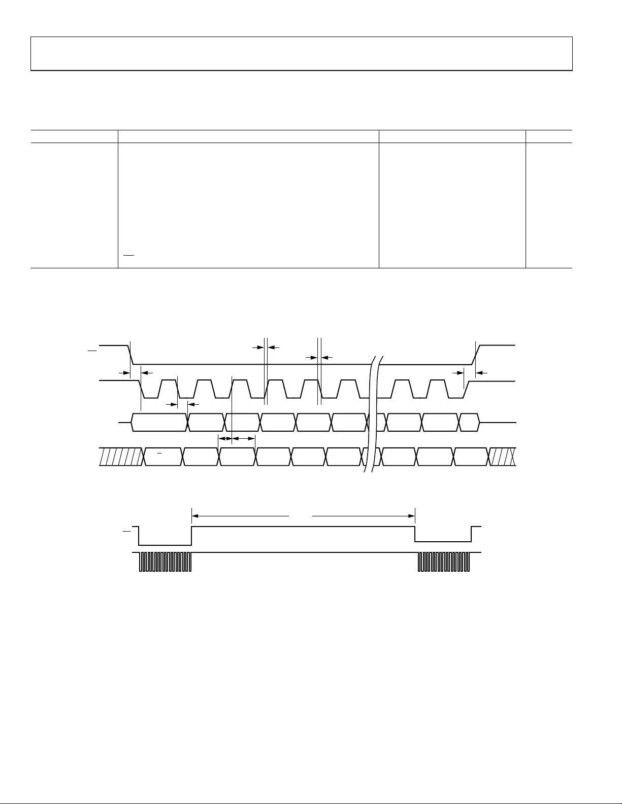
Figure 2. SPI Timing and Sequence
Figure 3. DIN Bit Sequence
Rev. B | Page 4 of 24

Data Sheet ADIS16227
Any Axis, Unpowered
2000 g
Operating Temperature Range
−40°C to +125°C
ABSOLUTE MAXIMUM RATINGS
Table 3.
Parameter Rating
Acceleration
Any Axis, Powered 2000 g
VDD to GND −0.3 V to +6.0 V
Digital Input Voltage to GND −0.3 V to +5.3 V
Digital Output Voltage to GND −0.3 V to +3.6 V
Analog Inputs to GND −0.3 V to +3.6 V
Table 4. Package Characteristics
Package Type θJA θJC Device Weight
14-Lead Module 31°C/W 11°C/W 6.5 grams
ESD CAUTION
Storage Temperature Range −65°C to +150°C
Stresses above those listed under Absolute Maximum Ratings
may cause permanent damage to the device. This is a stress
rating only; functional operation of the device at these or any
other conditions above those indicated in the operational
section of this specification is not implied. Exposure to absolute
maximum rating conditions for extended periods may affect
device reliability.
Rev. B | Page 5 of 24

ADIS16227 Data Sheet
14
13
12
11
10
9
8
7
6
5
4
3
2
1
PIN 13
PIN 1
PIN 2
a
X
a
Z
a
Y
TOP VIEW
LOOK THROUGH
PINS ARE NOT VISIBLE
FROM THIS VIEW
1. THE ARROWS ASSOCIATED WIT H a
X
, aY, AND a
Z
DEFINE THE DIRECTION OF
VELOCI TY CHANGE THAT P RODUCES A POSITIVE OUTPUT I N ACCE LERATIO N
OUTPUT REGISTERS.
2. MATING CONNECTOR E X AM P LE: SAMTE C P /N CLM-107-02-LM-D-A.
09425-004
PIN CONFIGURATION AND FUNCTION DESCRIPTIONS
Figure 4. Pin Configuration
Table 5. Pin Function Descriptions
Pin No. Mnemonic Type1 Description
1, 4, 9, 10 GND S Ground
2, 6 NC I No Connect
3 DIO2 I/O Digital Input/Output Line 2
5 DIO1 I/O Digital Input/Output Line 1
7
RST
I Reset, Active Low
8 VDD S Power Supply, 3.3 V
11 DIN I SPI, Data Input
12 DOUT O2 SPI, Data Output
13 SCLK I SPI, Serial Clock
14
1
S is supply, O is output, I is input, and I/O is input/output.
2
DOUT is an output when CS is low. When CS is high, DOUT is in a three-state, high impedance mode.
CS
I SPI, Chip Select
Rev. B | Page 6 of 24

Data Sheet ADIS16227
MOVABLE
FRAME
ACCELERATI ON
UNIT
FORCING
CELL
UNIT SENSING
CELL
MOVING
PLATE
FIXED
PLATES
PLATE
CAPACITORS
ANCHOR
ANCHOR
09425-005
TRIAXIAL
MEMS
SENSOR
CLOCK
CONTR
OLLER
CAPTURE
BUFFER
CO
NTROL
REGISTERS
SPI SIGNALS
SPI PORT
OUTPUT
REGISTERS
TEMP
SENSOR
ADC
09425-006
NONVOLATILE
FLASH MEMORY
(NO SPI ACCESS)
MANUAL
FLASH
BACKUP
START-UP
RESET
VOLATILE
SRAM
SPI ACCESS
09425-007
THEORY OF OPERATION
The ADIS16227 is a triaxial, wide bandwidth, vibration-sensing
system. It combines a triaxial MEMS accelerometer with a
sampling and advanced signal processing system. The SPIcompatible port and user register structure provide convenient
access to frequency domain vibration data and many user
controls.
SENSING ELEMENT
Digital vibration sensing in the ADIS16227 starts with a wide
bandwidth MEMS accelerometer core on each axis, which provides
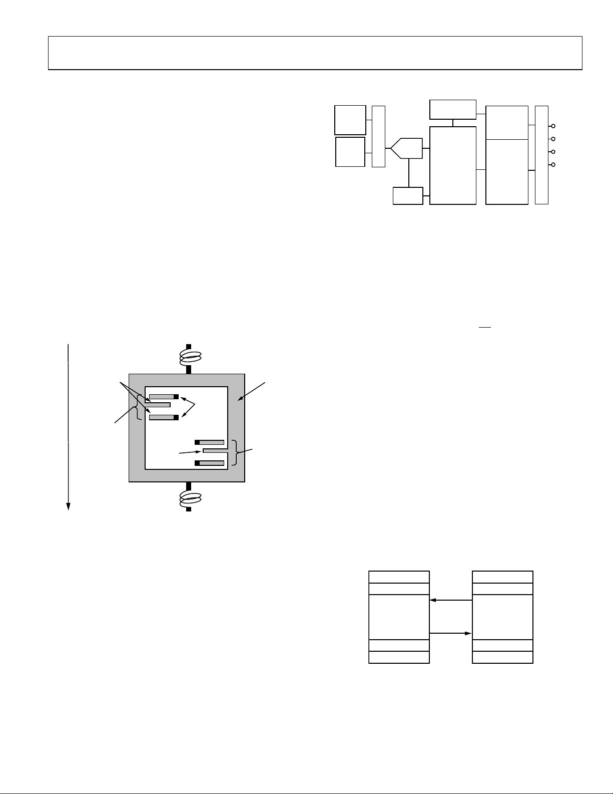
a linear motion-to-electrical transducer function. Figure 5 provides
a basic physical diagram of the sensing element and its response
to linear acceleration. It uses a fixed frame and a moving frame
to form a differential capacitance network that responds to linear
acceleration. Tiny springs tether the moving frame to the fixed
frame and govern the relationship between acceleration and
physical displacement. A modulation signal on the moving plate
feeds through each capacitive path into the fixed frame plates and
into a demodulation circuit, which produces the electrical signal
that is proportional to the acceleration acting on the device.
Figure 5. MEMS Sensor Diagram
SIGNAL PROCESSING
Figure 6 offers a simplified block diagram for the ADIS16227.
The signal processing stage includes time domain data capture,
digital decimation/filtering, windowing, FFT analysis, FFT
averaging, and record storage. See Figure 13 for more details on
the signal processing operation.
USER INTERFACE
SPI Interface
The user registers manage user access to both sensor data and
configuration inputs. Each 16-bit register has its own unique bit
assignment and two addresses: one for its upper byte and one for
its lower byte. Table 8 provides a memory map for each register,
along with its function and lower byte address. The data
collection and configuration command uses the SPI, which
consists of four wires. The chip select (
SPI interface, and the serial clock (SCLK) synchronizes the
serial data lines. Input commands clock into the DIN pin, one
bit at a time, on the SCLK rising edge. Output data clocks out of
the DOUT pin on the SCLK falling edge. When the SPI is used
as a slave device, the DOUT contents reflect the information
requested using a DIN command.
Dual Memory Structure
The user registers provide addressing for all input/output operations
in the SPI interface. The control registers use a dual memory
structure. The controller uses SRAM registers for normal
operation, including user-configuration commands. The flash
memory provides nonvolatile storage for control registers that
have flash backup (see Ta ble 8). Storing configuration data in
the flash memory requires a manual flash update command
(GLOB_CMD[6] = 1, DIN = 0xBE40). When the device powers
on or resets, the flash memory contents load into the SRAM, and
the device starts producing data according to the configuration
in the control registers.
Figure 6. Simplified Sensor Signal Processing Diagram
CS
) signal activates the
Figure 7. SRAM and Flash Memory Diagram
Rev. B | Page 7 of 24

ADIS16227 Data Sheet
V
V
K
BASIC OPERATION
The ADIS16227 uses a SPI for communication, which enables
a simple connection with a compatible, embedded processor
platform, as shown in Figure 8. The factory default configuration
for DIO1 provides a busy indicator signal that transitions low
when an event completes and data is available for user access.
Use the DIO_CTRL register (see Table 59) to reconfigure DIO1
and DIO2, if necessary.
DD
SYSTEM
PROCESSOR
SPI MASTER
SS
SCLK
MOSI
MISO
IRQ1 DIO1
IRQ2 DIO2
Figure 8. Electrical Hook-Up Diagram
14
13
11
12
5
3
+3.3
ADIS16227
CS
SCLK
DIN
DOUT
1 4 9 10
8
SPI SLAVE
09425-008
Table 6. Generic Master Processor Pin Names and Functions
Pin Name Function
SS
Slave select
IRQ1, IRQ2 Interrupt request inputs (optional)
MOSI Master output, slave input
MISO Master input, slave output
SCLK Serial clock
The ADIS16227 SPI interface supports full duplex serial
communication (simultaneous transmit and receive) and uses
the bit sequence shown in Figure 12. Table 7 provides a list of
the most common settings that require attention to initialize a
processor serial port for the ADIS16227 SPI interface.
Table 7. Generic Master Processor SPI Settings
Processor Setting Description
Master ADIS16227 operates as a slave.
SCLK Rate ≤ 2.25 MHz Bit rate setting.
SPI Mode 3 Clock polarity/phase
(CPOL = 1, CPHA = 1).
MSB-First Bit sequence.
16-Bit Shift register/data length.
Table 8 provides a list of user registers with their lower byte
addresses. Each register consists of two bytes that each have their
own, unique 7-bit addresses. Figure 9 relates each register’s bits
to their upper and lower addresses.
15 14 13 12 11 10 9 8 7 6 5 4 3 2 1 0
UPPER BYTE
LOWER BYTE
Figure 9. Generic Register Bit Definitions
SPI WRITE COMMANDS
User control registers govern many internal operations. The
DIN bit sequence in Figure 12 provides the ability to write to
these registers, one byte at a time. Some configuration changes
and functions require only one write cycle. For example, set
GLOB_CMD[11] = 1 (DIN = 0xBF08) to start a manual capture
sequence. The manual capture starts immediately after the last bit
clocks into DIN (16
th
SCLK rising edge). Other configurations may
require writing to both bytes.
CS
SCL
DIN
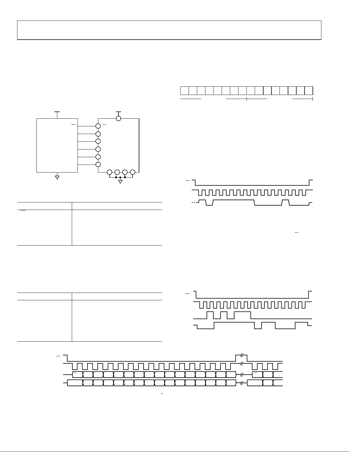
Figure 10. SPI Sequence for Manual Capture Start (DIN = 0xBF08)
SPI READ COMMANDS
A single register read requires two 16-bit SPI cycles that also use
R
the bit assignments in Figure 12. The first sequence sets
and communicates the target address (Bits[A6:A0]). Bits[D7:D0]
are don’t care bits for a read DIN sequence. DOUT clocks out the
requested register contents during the second sequence. The
second sequence can also use DIN to set up the next read. Figure 11
provides a signal diagram for all four SPI signals while reading
the PROD_ID register (see Table 63) pattern. In this diagram,
DIN = 0x5600 and DOUT reflect the decimal equivalent of 16,227.
CS
SCLK
DIN
DOUT
DOUT = 0011 1111 0110 0011 = 0x 3F63 = 16,227 = PROD_ID
Figure 11. Example SPI Read, PROD_ID, Second Sequence
/W = 0
09425-009
09425-010
09425-011
CS
SCLK
DIN
DOUT
NOTES
1. DOUT BITS ARE BASED ON THE PREVIOUS 16-BIT SEQUE NCE (R/W = 0).
R/W
A6 A5 A4 A3 A2 A1 A0 D7 D6 D5 D4 D3 D2 D1 D0
R/W
A6 A5
DB0DB1DB2DB3DB4DB5DB6DB7DB8DB9DB10DB11DB12DB13DB14DB15
DB15
DB13DB14
09425-012
Figure 12. Example SPI Read Sequence
Rev. B | Page 8 of 24
 Loading...