Digital Tri-Axial Vibration Sensor
FEATURES
Tri-axial vibration sensing: ±70 g range
Wide bandwidth: 14 kHz
Programmable digital filters, low-pass/band-pass options
Data capture function
3-channels, 1024 samples each, 72.9 kSPS sample rate
Capture modes for managing machine life
Manual: early baseline characterization/validation
Automatic: periodic check for midlife performance shifts
Event: end-of-life monitoring for critical conditions
Extended: triple the record length for a single axis
Digital temperature, power supply measurements
Programmable operation and control
Capture mode and sample rate
I/O: data ready, alarm, capture trigger, general-purpose
Four alarm settings with threshold limits
Digitally activated self-test
SPI-compatible serial interface
Serial number and device ID
Single-supply operation: 3.15 V to 3.6 V
Operating temperature range: −40°C to +125°C
15 mm × 15 mm × 15 mm package with flexible connector
APPLICATIONS
Vibration analysis
Shock detection and event capture
Condition monitoring
Machine health
Instrumentation, diagnostics
Safety, shutoff sensing
Security sensing, tamper detection
FUNCTIONAL BLOCK DIAGRAM
ADIS16223
GENERAL DESCRIPTION
The ADIS16223 iSensor® is a tri-axial, digital vibration sensor
system that combines industry-leading iMEMS® sensing technology
with signal processing, data capture, and a convenient serial
peripheral interface (SPI). The SPI and data buffer structure
provide convenient access to wide bandwidth sensor data. The
22 kHz sensor resonance and 72.9 kSPS sample rate provide a
frequency response that is suitable for machine-health applications.
The programmable digital filter offers low-pass and band-pass
configuration options.
An internal clock drives the data sampling system during a data
capture event, which eliminates the need for an external clock
source. The data capture function has four different modes that
offer several capture trigger options to meet the needs of many
different applications.
The ADIS16223 also offers a digital temperature sensor, digital
power supply measurements, and peak output capture.
The ADIS16223 is available in a 15 mm × 15 mm × 15 mm module
with a threaded hole for stud mounting with a 10-32 UNF screw.
The dual-row, 1 mm, 14-pin, flexible connector enables simple
user interface and installation. It has an extended operating
temperature range of −40°C to +125°C.
VDDRSTDIO1 DIO2
CLOCK
INPUT/
OUTPUT
CONTROLLERADC
FILTER
CAPTURE
BUFFER
SELF-TEST
TRIAXIAL
MEMS
SENSOR
TEMP
SENSOR
ADIS16223
Rev. 0
Information furnished by Analog Devices is believed to be accurate and reliable. However, no
responsibility is assumed by Analog Devices for its use, nor for any infringements of patents or other
rights of third parties that may result from its use. Specifications subject to change without notice. No
license is granted by implication or otherwise under any patent or patent rights of Analog Devices.
Trademarks and registered trademarks are the property of their respective owners.
ALARMS
Figure 1.
One Technology Way, P.O. Box 9106, Norwood, MA 02062-9106, U.S.A.
Tel: 781.329.4700 www.analog.com
Fax: 781.461.3113 ©2010 Analog Devices, Inc. All rights reserved.
MANAGEMENT
USER
CONTROL
REGISTERS
OUTPUT
DATA
REGISTERS
POWER
SPI
PORT
GND
CS
SCLK
DIN
DOUT
09098-001

ADIS16223
TABLE OF CONTENTS
Features .............................................................................................. 1
Applications ....................................................................................... 1
General Description ......................................................................... 1
Functional Block Diagram .............................................................. 1
Revision History ............................................................................... 2
Specifications ..................................................................................... 3
Timing Specifications .................................................................. 4
Absolute Maximum Ratings ............................................................ 5
ESD Caution .................................................................................. 5
Pin Configuration and Function Descriptions ............................. 6
Theory of Operation ........................................................................ 7
Sensing Element ........................................................................... 7
Data Sampling and Processing ................................................... 7
User Interface ................................................................................ 7
Basic Operation ................................................................................. 8
SPI Write Commands .................................................................. 8
SPI Read Commands ................................................................... 8
Data Collection ........................................................................... 10
Reading Data from the Capture Buffer ................................... 10
Output Data Registers ................................................................ 10
Capture/Alarm Configuration ...................................................... 11
Manual Mode .............................................................................. 11
Automatic Mode ......................................................................... 11
Event Mode ................................................................................. 12
Extended Mode ........................................................................... 12
Power-Down Control ................................................................ 12
Automatic Flash Back-Up Control .......................................... 12
Capture Times ............................................................................ 12
Alarms .............................................................................................. 13
System Tools .................................................................................... 14
Global Commands ..................................................................... 14
Input/Output Functions ............................................................ 14
Self-Test ....................................................................................... 15
Device Identification .................................................................. 15
Flash Memory Management ..................................................... 15
Digital Signal Processing ............................................................... 16
Low-Pass Filter ............................................................................ 16
Band-Pass Filter .......................................................................... 16
Offset Adjustment ...................................................................... 16
Applications Information .............................................................. 17
Getting Started ............................................................................ 17
Interface Board ........................................................................... 17
Outline Dimensions ....................................................................... 18
Ordering Guide .......................................................................... 18
REVISION HISTORY
6/10—Revision 0: Initial Version
Rev. 0 | Page 2 of 20

ADIS16223
SPECIFICATIONS
TA = −40°C to +125°C, VDD = 3.3 V, unless otherwise noted.
Table 1.
Parameter Test Conditions/Comments Min Typ Max Unit
ACCELEROMETERS
Measurement Range TA = 25°C −70 +70
Sensitivity TA = 25°C 4.768 mg/LSB
Sensitivity Error TA = 25°C ±5 %
Nonlinearity With respect to full scale ±0.2 ±2 %
Cross Axis Sensitivity 2.6 %
Alignment Error With respect to package 1.5 Degree
Offset Error TA = 25°C −19.1 +19.1
Offset Temperature Coefficient 5 mg/°C
Output Noise TA = 25°C, Register AVG_CNT = 0x0000 477 mg rms
Output Noise Density TA = 25°C, 10 Hz to 1 kHz 3.3 mg/√Hz
Bandwidth X/Y axes, ±5% flatness 7.75 kHz
X/Y axes, ±10% flatness 9.0 kHz
Z-axis, ±5% flatness 13 kHz
Z-axis, ±10% flatness 14.25 kHz
Sensor Resonant Frequency 22 kHz
Self-Test Response 3669 5243 6815 LSB
LOGIC INPUTS1
Input High Voltage, V
Input Low Voltage, V
Logic 1 Input Current, I
Logic 0 Input Current, I
All Except RST
RST
2.0 V
INH
0.8 V
INL
V
INH
V
INL
= 3.3 V ±0.2 ±1 μA
IH
= 0 V
IL
−40 −60 μA
−1 mA
Input Capacitance, CIN 10 pF
DIGITAL OUTPUTS1
Output High Voltage, VOH I
Output Low Voltage, VOL I
= 1.6 mA 2.4 V
SOURCE
= 1.6 mA 0.4 V
SINK
FLASH MEMORY
Endurance2 10,000 Cycles
Data Retention3 T
= 85°C 20 Years
J
START-UP TIME4
Initial Startup 179 ms
Reset Recovery5
pulse low or Register GLOB_CMD[7] = 1
RST
54 ms
Sleep Mode Recovery 2.5 ms
CONVERSION RATE Register AVG_CNT = 0x0000 72.9 kSPS
Clock Accuracy 3 %
POWER SUPPLY Operating voltage range, VDD 3.15 3.3 3.6 V
Power Supply Current Capture mode, TA = 25°C 43 52 mA
Sleep mode, TA = 25°C 230 μA
1
The digital I/O signals are 5 V tolerant.
2
Endurance is qualified as per JEDEC Standard 22, Method A117, and measured at −40°C, +25°C, +85°C, and +125°C.
3
Retention lifetime equivalent at junction temperature (TJ) = 85°C as per JEDEC Standard 22, Method A117. Retention lifetime decreases with junction temperature. See
Figure 15.
4
The start-up times presented do not include the data capture time, which is dependent on the AVG_CNT register settings.
5
RST
The
pin must be held low for at least 15 ns.
g
g
Rev. 0 | Page 3 of 20

ADIS16223
TIMING SPECIFICATIONS
TA = 25°C, VDD = 3.3 V, unless otherwise noted.
Table 2.
Parameter Description Min1 Typ Max Uni t
f
SCLK frequency 0.01 2.25 MHz
SCLK
t
Stall period between data, between 16th and 17th SCLK 15.4 μs
STALL
tCS Chip select to SCLK edge 48.8 ns
t
DOUT valid after SCLK edge 100 ns
DAV
t
DIN setup time before SCLK rising edge 24.4 ns
DSU
t
DIN hold time after SCLK rising edge 48.8 ns
DHD
tSR SCLK rise time 12.5 ns
tSF SCLK fall time 12.5 ns
tDF, tDR DOUT rise/fall times 5 12.5 ns
t
SFS
1
Guaranteed by design, not tested.
high after SCLK edge
CS
Timing Diagrams
CS
t
CS
SCLK
t
SR
123456 1516
t
DAV
t
SF
5 ns
t
SFS
DOUT
DIN
MSB DB14
t
R/W A5A6 A4 A3 A2
DB13 DB12 DB10DB11 DB2 LSBDB1
t
DSU
DHD
D2
D1 LSB
09098-002
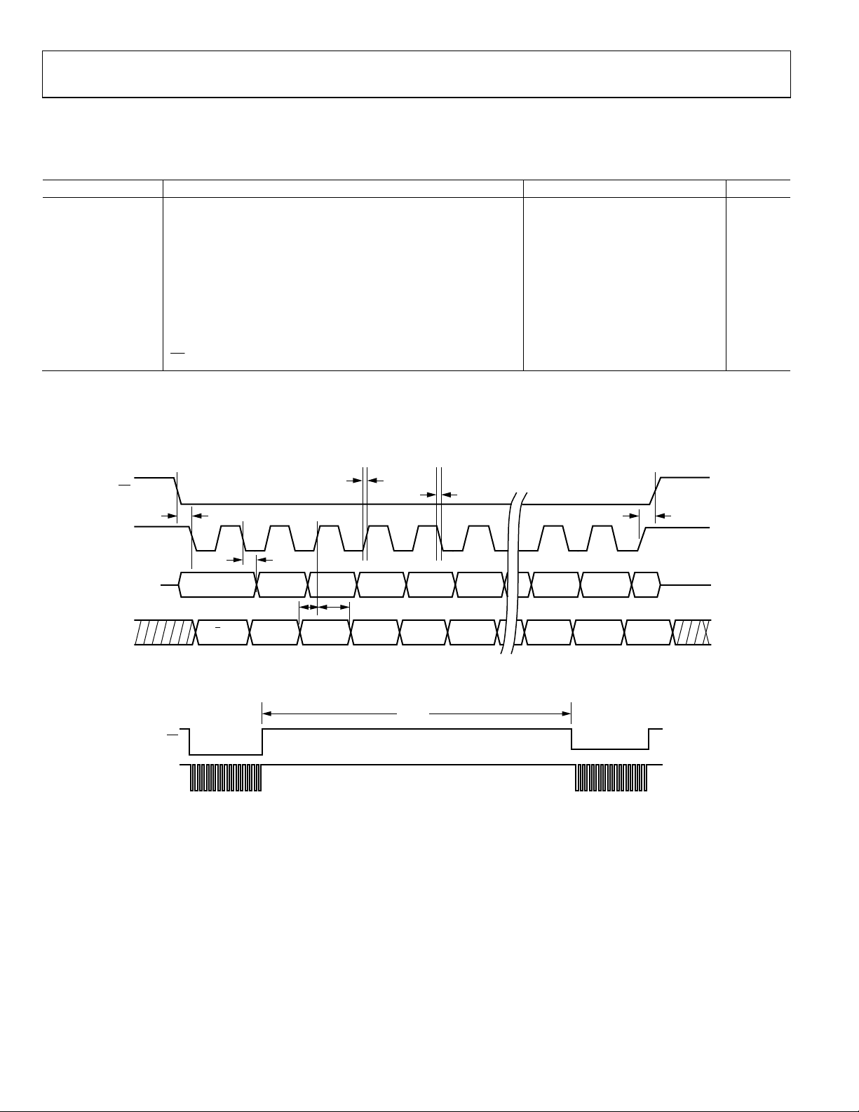
Figure 2. SPI Timing and Sequence
t
STALL
CS
SCLK
09098-003
Figure 3. DIN Bit Sequence
Rev. 0 | Page 4 of 20

ADIS16223
ABSOLUTE MAXIMUM RATINGS
Table 3.
Parameter Rating
Acceleration
Any Axis, Unpowered 2000 g
Any Axis, Powered 2000 g
VDD to GND −0.3 V to +6.0 V
Digital Input Voltage to GND −0.3 V to +5.3 V
Digital Output Voltage to GND −0.3 V to VDD + 0.3 V
Analog Inputs to GND −0.3 V to +3.6 V
Operating Temperature Range −40°C to +125°C
Storage Temperature Range −65°C to +150°C
Stresses above those listed under Absolute Maximum Ratings
may cause permanent damage to the device. This is a stress
rating only; functional operation of the device at these or any
other conditions above those indicated in the operational
section of this specification is not implied. Exposure to absolute
maximum rating conditions for extended periods may affect
device reliability.
Table 4. Package Characteristics
Package Type θJA θ
14-Lead Module 31°C/W 11°C/W 6.5 grams
Device Weight
JC
ESD CAUTION
Rev. 0 | Page 5 of 20

ADIS16223
PIN CONFIGURATION AND FUNCTION DESCRIPTIONS
a
Y
a
Z
a
X
PIN 2
PIN 13
1. THE ARROW S ASSOCIATED WITH a
VELOCITY CHANGE THAT P RODUCES A POSITIVE OUT PUT IN ACCELERAT ION
OUTPUT REGISTERS.
2. MATING CONNECTOR E XAMPLE: S AMTEC P/N CLM -107-02-LM-D-A.
PIN 1
, aY, AND aZ DEFINE THE DIRECTION OF
X
TOP VIEW
“LOOK THRO UG H”
PINS ARE NOT V ISIBLE
FROM THIS VIEW
141312111098765432
1
09098-004
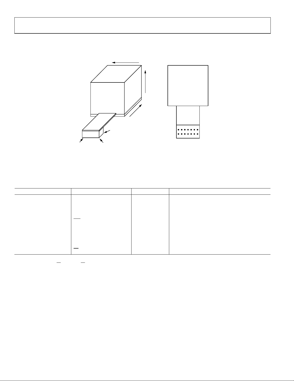
Figure 4. Pin Configuration
Table 5. Pin Function Descriptions
Pin No. Mnemonic Type1 Description
1, 4, 9, 10 GND S Ground
2, 6 NC I No Connect
3 DIO2 I/O Digital Input/Output Line 2
5 DIO1 I/O Digital Input/Output Line 1
7
RST
I Reset, Active Low
8 VDD S Power Supply, 3.3 V
11 DIN I SPI, Data Input
12 DOUT O2 SPI, Data Output
13 SCLK I SPI, Serial Clock
14
1
S is supply, O is output, I is input, and I/O is input/output.
2
DOUT is an output when CS is low. When CS is high, DOUT is in a three-state, high impedance mode.
CS
I SPI, Chip Select
Rev. 0 | Page 6 of 20
 Loading...