High-Accuracy, Dual-Axis
Digital Inclinometer and Accelerometer
FEATURES
Dual-mode inclinometer system
Dual-axis, horizontal operation, ±90°
Single-axis, vertical operation, ±180°
High accuracy, 0.1°
14-bit digital inclination data, 0.025° resolution
14-bit digital acceleration data, 0.244 mg resolution
±1.7 g accelerometer measurement range
12-bit digital temperature sensor output
Digitally controlled bias calibration
Digitally controlled sample rate
Digitally controlled frequency response
Dual alarm settings with rate/threshold limits
Auxiliary digital I/O
Digitally activated self-test
Digitally activated low power mode
SPI-compatible serial interface
Auxiliary 12-bit ADC input and DAC output
Single-supply operation: 3.0 V to 3.6 V
3500 g powered shock survivability
VDD
GND
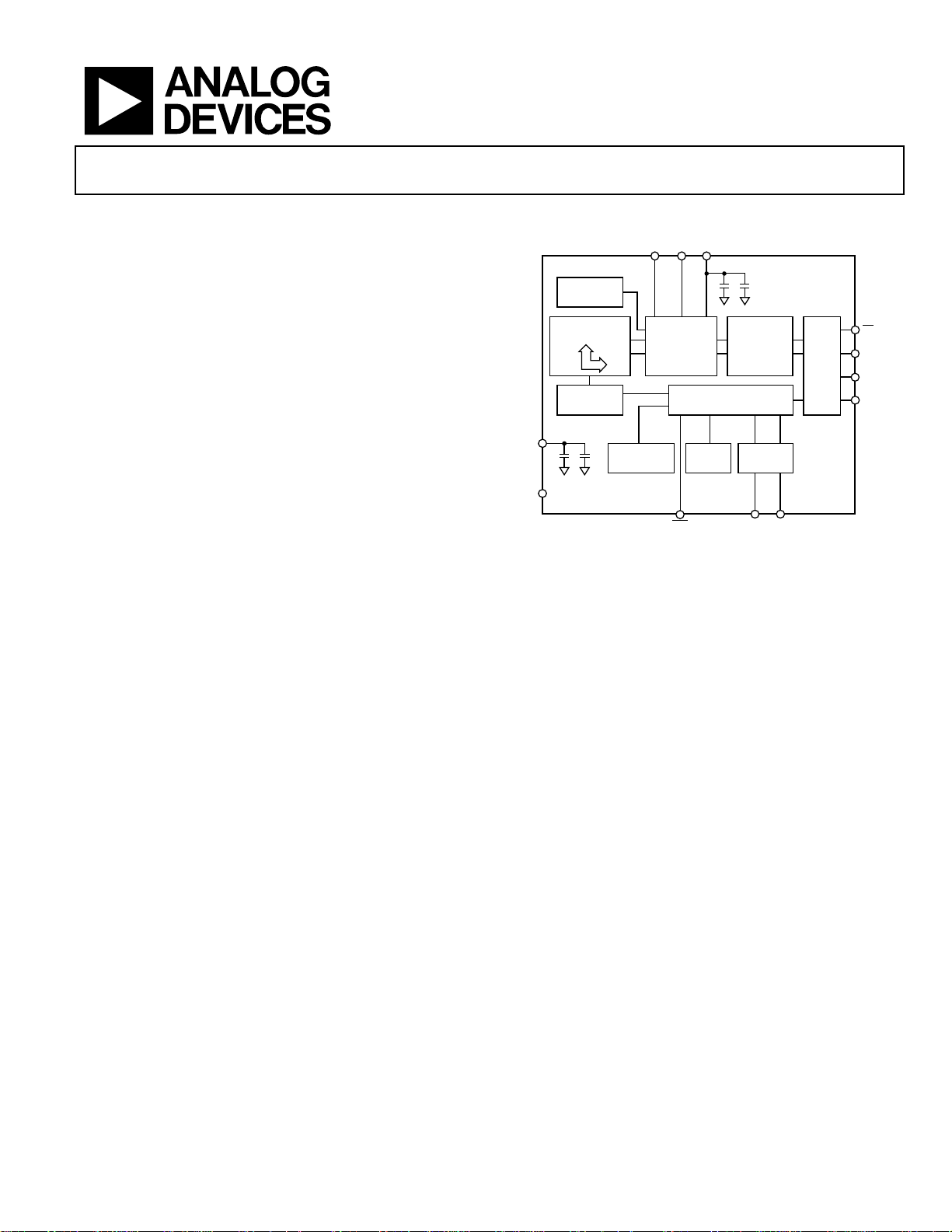
FUNCTIONAL BLOCK DIAGRAM
AUX
AUX
TEMPERATURE
SENSOR
DUAL-AXIS
ACCELEROMETER
SELF-TEST
MANAGEMENT
ADC
POWER
VREF
DAC
SIGNAL
CONDITIONI NG
AND
CONVERSION
RST DIO1 DIO2
Figure 1.
ALARMS
CALIBRATION
PROCESSING
DIGITAL
CONTROL
DIGIT AL
AUXILIARY
ADIS16209
ADIS16209
AND
SPI
PORT
I/O
CS
SCLK
DIN
DOUT
07096-001
APPLICATIONS
Platform control, stabilization, and alignment
Tilt sensing, inclinometers, leveling
Motion/position measurement
Monitor/alarm devices (security, medical, safety)
Navigation
GENERAL DESCRIPTION
The ADIS16209 is a high-accuracy, digital inclinometer that
accommodates both single axis (±180°) and dual-axis (±
peration. The standard supply voltage (3.3 V) and serial
o
peripheral interface (SPI) serial interface enable simple
integration into most industrial system designs. A simple
internal register structure handles all output data and
configuration features. This includes access to the following
output data: calibrated acceleration, accurate incline angles,
power supply, internal temperature, auxiliary analog and digital
input signals, diagnostic error flags, and programmable alarm
conditions.
90°)
Configurable operating parameters include sample rate,
power management, digital filtering, auxiliary analog and
digital output, offset/null adjustment, and self-test for sensor
mechanical structure.
The ADIS16209 is available in a 9.2 mm × 9.2 mm × 3.9 mm
LGA package that operates over a temperature range of −40°C
to +125°C. It can be attached using standard RoHS-compliant
solder reflow processes.
Rev. 0
Information furnished by Analog Devices is believed to be accurate and reliable. However, no
responsibility is assumed by Analog Devices for its use, nor for any infringements of patents or other
rights of third parties that may result from its use. Specifications subject to change without notice. No
license is granted by implication or otherwise under any patent or patent rights of Analog Devices.
Trademarks and registered trademarks are the property of their respective owners.
One Technology Way, P.O. Box 9106, Norwood, MA 02062-9106, U.S.A.
Tel: 781.329.4700 www.analog.com
Fax: 781.461.3113 ©2008 Analog Devices, Inc. All rights reserved.

ADIS16209
TABLE OF CONTENTS
Features .............................................................................................. 1
Applications ....................................................................................... 1
Functional Block Diagram .............................................................. 1
General Description ......................................................................... 1
Revision History ............................................................................... 2
Specifications ..................................................................................... 3
Timing Specifications .................................................................. 5
Timing Diagrams .......................................................................... 5
Absolute Maximum Ratings ............................................................ 6
Thermal Resistance ...................................................................... 6
ESD Caution .................................................................................. 6
REVISION HISTORY
3/08—Revison 0: Initial Version
Pin Configuration and Function Descriptions ..............................7
Recommended Pad Geometry ....................................................7
Typical Performance Characteristics ..............................................8
Theory of Operation ...................................................................... 10
Basic Operation .............................................................................. 11
Output Data Registers ............................................................... 12
Operation Control Registers ..................................................... 12
Calibration Registers .................................................................. 14
Alarm Registers .......................................................................... 14
Outline Dimensions ....................................................................... 16
Ordering Guide .......................................................................... 16
Rev. 0 | Page 2 of 16

ADIS16209
SPECIFICATIONS
TA = 25°C, VDD = 3.3 V, tilt = 0°, unless otherwise noted.
Table 1.
Parameter Conditions Min Typ Max Unit
HORIZONTAL INCLINE Each axis
Input Range ±90 Degrees
Relative Accuracy ±30° from horizon, AVG_CNT = 0x08 ±0.1 Degrees
Sensitivity ±30° from horizon 0.025 °/LSB
VERTICAL ROTATION Rotational plane within ±30 degrees of vertical
Input Range −180 +180 Degrees
Relative Accuracy 360° of rotation ±0.25 Degrees
Sensitivity −40°C to +85°C 0.025 °/LSB
ACCELEROMETER Each axis
Input Range
Nonlinearity
Alignment Error X sensor to Y sensor ±0.1 Degrees
Cross Axis Sensitivity ±2 %
Sensitivity −40°C to +85°C, VDD = 3.0 V to 3.6 V 0.243 0.244 0.245 mg/LSB
ACCELEROMETER NOISE PERFORMANCE
Output Noise AVG_CNT = 0x00 1.7 mg rms
Noise Density AVG_CNT = 0x00 0.19 mg/√Hz rms
ACCELEROMETER FREQUENCY RESPONSE
Sensor Bandwidth 50 Hz
Sensor Resonant Frequency 5.5 kHz
ACCELEROMETER SELF-TEST STATE
Output Change When Active At 25°C 706 1343 1973 LSB
TEMPERATURE SENSOR
Output at 25°C 1278 LSB
Scale Factor −0.47 °C/LSB
ADC INPUT
Resolution 12 Bits
Integral Nonlinearity (INL) ±2 LSB
Differential Nonlinearity (DNL) ±1 LSB
Offset Error ±4 LSB
Gain Error ±2 LSB
Input Range 0 2.5 V
Input Capacitance During acquisition 20 pF
ON-CHIP VOLTAGE REFERENCE 2.5 V
Accuracy At 25°C −10 +10 mV
Reference Temperature Coefficient ±40 ppm/oC
Output Impedance 70 Ω
DAC OUTPUT 5 kΩ/100 pF to GND
Resolution 12 Bits
Relative Accuracy For Code 101 to Code 4095 4 LSB
Differential Nonlinearity 1 LSB
Offset Error ±5 mV
Gain Error ±0.5 %
Output Range 0 to 2.5 V
Output Impedance 2 Ω
Output Settling Time 10 µs
1
1
2
25°C ±1.7
% of full scale ±0.1 ±0.2 %
g
Rev. 0 | Page 3 of 16

ADIS16209
Parameter Conditions Min Typ Max Unit
LOGIC INPUTS
Input High Voltage, V
Input Low Voltage, V
Logic 1 Input High Current, I
Logic 0 Input Low Current, I
All except
RST
RST
3
Input Capacitance, CIN 10 pF
DIGITAL OUTPUTS
Output High Voltage, VOH I
Output Low Voltage, VOL I
SLEEP TIMER
Timeout Period
START-UP TIME
5
Power-On Fast mode, SMPL_PRD ≤ 0x07 150 ms
Normal mode, SMPL_PRD ≥ 0x08 190 ms
Reset Recovery Fast mode, SMPL_PRD ≤ 0x07 30 ms
Normal mode, SMPL_PRD ≥ 0x08 70 ms
Sleep Mode Recovery 2.5 ms
FLASH MEMORY
Endurance
6
Data Retention
CONVERSION RATE SETTING 1.04 2731 SPS
POWER SUPPLY
Operating Voltage Range 3.0 3.3 3.6 V
Power Supply Current Normal mode, SMPL_PRD ≥ 0x08 11 14 mA
Fast mode, SMPL_PRD ≤ 0x07 36 42 mA
Sleep mode, −40°C to +85°C 140 350 µA
1
Guaranteed by iMEMS® packaged part testing, design, and/or characterization.
2
Self-test response changes as the square of VDD.
3
RST
The
pin has an internal pull-up.
4
Guaranteed by design.
5
The times presented in this section do not include the sensor’s transient response time, which is associated with a 50 Hz single-pole system. System accuracy goals
should be given consideration when determining the amount of time it takes to start acquiring accurate readings. These times do not include the time it takes to
arrive at thermal stability, which can also introduce transient errors.
6
Endurance is qualified as per JEDEC Standard 22 Method A117 and measured at −40°C, +25°C, +85°C, and +125°C.
7
Retention lifetime equivalent at junction temperature (TJ) 55°C as per JEDEC Standard 22 Method A117. Retention lifetime decreases with junction temperature.
2.0 V
INH
0.8 V
INL
CS
For
signal when used to wake up from sleep mode
VIH = 3.3 V ±0.2 ±10 µA
INH
V
INL
= 0 V
IL
−40 −60 A
0.55 V
−1 mA
= 1.6 mA 2.4 V
SOURCE
= 1.6 mA 0.4 V
SINK
4
0.5 128 Seconds
Time until data is available
20,000 Cycles
7
TJ = 85°C 20 Years
Rev. 0 | Page 4 of 16

ADIS16209
K
TIMING SPECIFICATIONS
TA = 25°C, VDD = 3.3 V, tilt = 0°, unless otherwise noted.
Table 2.
Parameter Description Min1 Typ Max Unit
f
Fast mode, SMPL_PRD ≤ 0x07 (fS ≥ 546 Hz)2 0.01 2.5 MHz
SCLK
Normal mode, SMPL_PRD ≥ 0x08 (fS ≤ 482 Hz)2 0.01 1.0 MHz
t
Chip select period, fast mode, SMPL_PRD ≤ 0x07 (fS ≥ 546 Hz)2 40 s
DATARATE
tCS Chip select to clock edge 48.8 ns
t
Data output valid after SCLK edge 100 ns
DAV
t
Data input setup time before SCLK rising edge 24.4 ns
DSU
t
Data input hold time after SCLK rising edge 48.8 ns
DHD
tDF Data output fall time 5 12.5 ns
tDR Data output rise time 5 12.5 ns
t
SFS
1
Guaranteed by design, not tested.
2
Note that fS means internal sample rate.
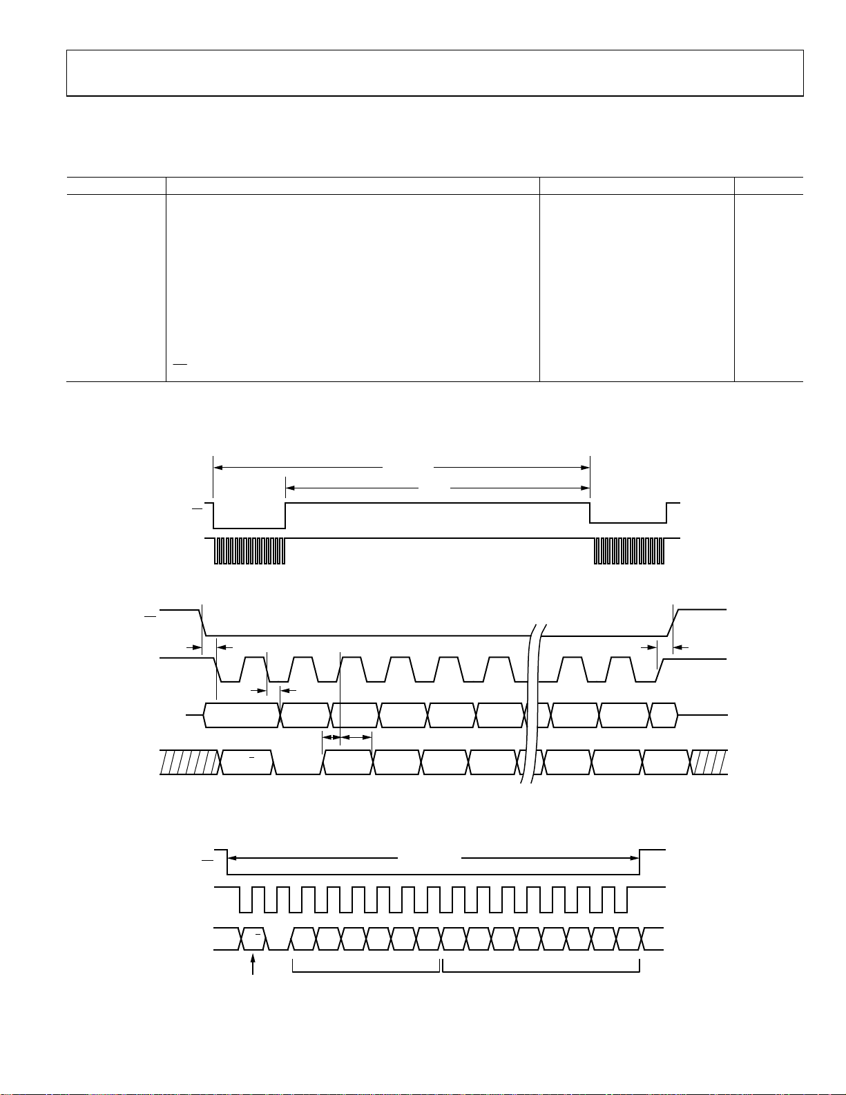
TIMING DIAGRAMS
Chip select period, normal mode, SMPL_PRD ≥ 0x08 (fS ≤ 482 Hz)2 100 s
high after SCLK edge
CS
t
DATARATE
t
STALL
5 ns
CS
SCLK
t
=
t
– 16/
STALL
DATARATE
f
SCLK
07096-002
Figure 2. SPI Chip Select Timing
CS
SCLK
DOUT
DIN
t
CS
1 2 3 4 5 6 15 16
t
DAV
MSB DB14
W/R A5 A4 A3 A2
DB13 DB12 DB10DB11 DB2 LSBDB1
t
DSU
t
DHD
D2
D1 L SB
t
SFS
07096-003
Figure 3. SPI Timing
(Utilizing SPI Settings Typically Identified as Phase = 1, Polarity = 1)
CS
SCL
DATA FRAME
DIN
W/R A5 A4 A3 A2 A1 A0 DC7 DC6 DC5 DC4 DC3 DC2 DC1 DC0
WRITE = 1
READ = 0
REGISTER ADDRESS DATA FOR WRITE COMMANDS
DON’T CARE FO R READ COMMANDS
07096-004
Figure 4. DIN Bit Sequence
Rev. 0 | Page 5 of 16
 Loading...