Digital Output, High Precision
www.BDTIC.com/ADI
FEATURES
Low noise density: 0.0125o/sec/√Hz
Industry-standard serial peripheral interface (SPI)
24-bit digital resolution
Dynamic range: ±250
Z-axis, yaw rate response
Bandwidth, adjustable: 300 Hz
Turn-on time: 35 ms
Digital self-test
High vibration rejection
High shock survivability
Embedded temperature sensor output
Precision voltage reference output
5 V single-supply operation
−40°C to +85°C
APPLICATIONS
Guidance and control
Instrumentation
Inertial measurement units (IMU)
Platform stabilization
Navigation
o
/sec
Angular Rate Sensor
ADIS16130
GENERAL DESCRIPTION
The ADIS16130 is a low noise, digital output angular rate sensor
(gyroscope) that provides an output response over the complete
dynamic range of ±250
Its industry-standard serial interface and register structure provide
ple interface that is supported by most MCU, DSP, and FPGA
a sim
platforms.
By implementing a unique design, the device provides superior
ability over variations in temperature, voltage, linear acceleration,
st
vibration, and next-level assembly. In addition, the surface-micromachining technology used to manufacture the device is the
same high volume BiMOS process used by Analog Devices, Inc.,
for its high reliability automotive sensor products.
Features include a temperature output that provides critical
info
rmation for system-level calibrations and a digital self-test
feature that exercises the mechanical structure of the sensor and
enables system-level diagnostics.
The package configuration is a 36 mm × 44 mm × 16 mm
mo
dule with a standard 24-lead connector interface.
o
/sec.
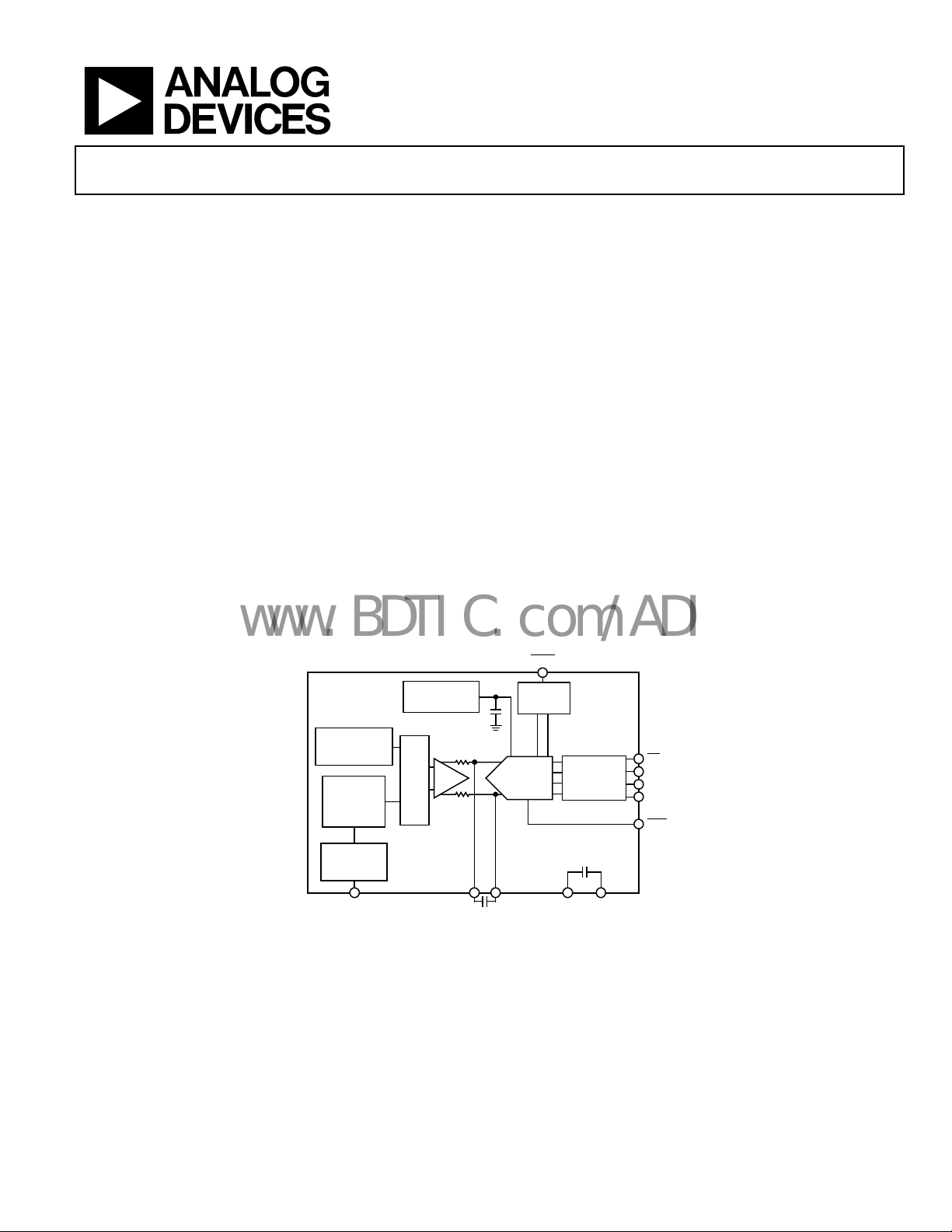
FUNCTIONAL BLOCK DIAGRAM
SYNC
ADIS16130
TEMPERATURE
SENSOR
MEMS
ANGULAR
RATE
SENSOR
SELF-TEST
ST ROA1 ROA2 VCC GND
REFERENCE
2:1
MUX
Figure 1.
SYNC
24-BIT
Σ-Δ ADC
SERIAL
INTERFACE
CS
SCLK
SDI
SDO
RDY
07238-001
Rev. A
Information furnished by Analog Devices is believed to be accurate and reliable. However, no
responsibility is assumed by Anal og Devices for its use, nor for any infringements of patents or ot her
rights of third parties that may result from its use. Specifications subject to change without notice. No
license is granted by implication or otherwise under any patent or patent rights of Analog Devices.
Trademarks and registered trademarks are the property of their respective owners.
One Technology Way, P.O. Box 9106, Norwood, MA 02062-9106, U.S.A.
Tel: 781.329.4700 www.analog.com
Fax: 781.461.3113 ©2008 Analog Devices, Inc. All rights reserved.

ADIS16130
www.BDTIC.com/ADI
TABLE OF CONTENTS
Features .............................................................................................. 1
Applications....................................................................................... 1
General Description ......................................................................... 1
Functional Block Diagram .............................................................. 1
Revision History ............................................................................... 2
Specifications..................................................................................... 3
Timing Specifications .................................................................. 4
Absolute Maximum Ratings............................................................ 6
Thermal Resistance ...................................................................... 6
ESD Caution.................................................................................. 6
Pin Configuration and Function Descriptions............................. 7
REVISION HISTORY
3/08—Rev. 0 to Rev. A
Changes to Figure 15...................................................................... 10
Changes to Ordering Guide.......................................................... 13
1/08—Revision 0: Initial Version
Typical Perf or m an c e Chara c t e risti c s ..............................................8
Basic Operation .................................................................................9
Quick Start .....................................................................................9
Configuration Options .............................................................. 10
Control Registers............................................................................ 11
Control Register Details ............................................................ 11
Applications Information.............................................................. 12
Achieving Optimal Noise Performance .................................. 12
Second-Level Assembly ............................................................. 12
Outline Dimensions ....................................................................... 13
Ordering Guide .......................................................................... 13
Rev. A | Page 2 of 16

ADIS16130
www.BDTIC.com/ADI
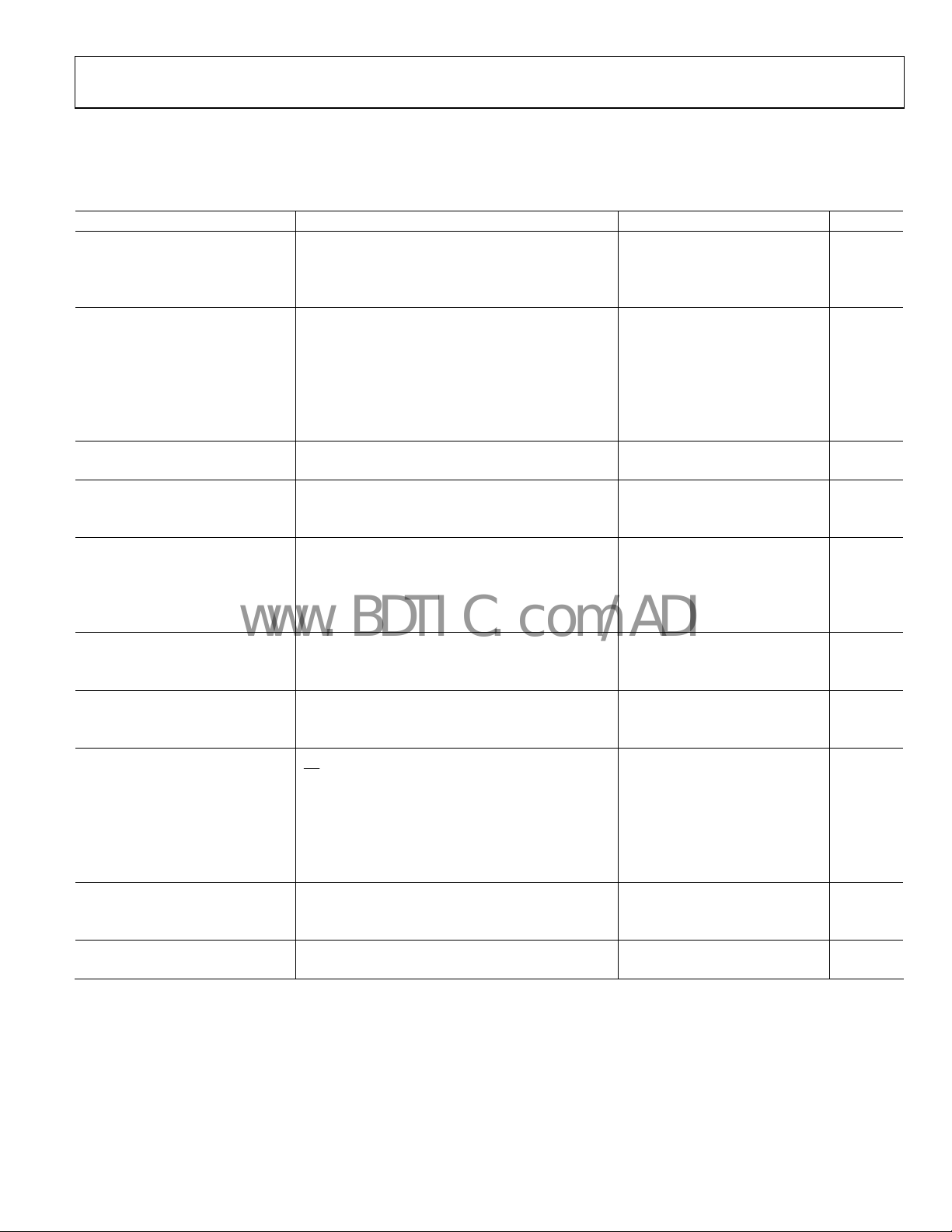
SPECIFICATIONS
TA = 25°C, VCC = 5 V, angular rate = 0°/sec, C
= 0 μF, ±1 g, unless otherwise noted.
OUT
Table 1.
Parameter Conditions Min
1
Typ Max
1
Unit
SENSITIVITY Clockwise rotation is positive output (see Figure 5)
Dynamic Range
2
Full-scale range over specified operating conditions ±250 °/sec
Initial 22,548 23,488 24,428 LSB/°/sec
Nonlinearity Best-fit straight line 0.04 % of FS
NULL
Initial Null ±1σ ±3 °/sec
In-Run Bias Stability 1σ 0.0016 °/sec
Angle Random Walk 1σ 0.56 °/√Hr
Turn-On Time Power on to ±0.5°/sec of final value, 80 Hz bandwidth 35 ms
Linear Acceleration Effect Any axis 0.05 °/sec/g
Voltage Sensitivity VCC = 4.75 V to 5.25 V 0.2 °/sec/V
NOISE PERFORMANCE
Rate Noise Density
3
0.0125 °/sec/√Hz
FREQUENCY RESPONSE
Bandwidth −3 dB frequency with no external capacitance 300 Hz
Sensor Resonant Frequency 14 kHz
SELF-TEST INPUTS
ST RATEOUT Response
4
ST pins from Logic 0 to Logic 1 65 75 85 °/sec
Logic 1 Input Voltage Standard high logic level definition 3.3 V
Logic 0 Input Voltage Standard low logic level definition 1.7 V
Input Impedance To GND 3.13 kΩ
TEMPERATURE SENSOR
Output at 298 K (25°C) 8,388,608 LSB
Scale Factor 14,093 LSB/°C
DIGITAL OUTPUTS
Output Low Voltage (VOL) 0.4 V
Output High Voltage (VOH) 4 V
DIGITAL INPUTS
Input Current
CS
10 μA
All others 1 μA
Input Capacitance 5 pF
VT+ 1.4 2 V
VT− 0.8 1.4 V
(VT+) – (VT−) 0.3 0.85 V
POWER SUPPLY
Operating Voltage Range 4.75 5.00 5.25 V
Quiescent Supply Current I
= 0 mA, 5 V 73 85 mA
OUT
TEMPERATURE RANGE
Operating Range –40 +85 °C
1
All minimum and maximum specifications are guaranteed. Typical specifications are not tested or guaranteed.
2
Dynamic range is the maximum full-scale measurement range possible, including output swing range, initial offset, sensitivity, offset drift, and sensitivity drift at 4.75 V
to 5.25 V supplies.
3
Resulting bias stability is <0.01°/sec.
4
Self-test response varies with temperature, see Figure 12.
Rev. A | Page 3 of 16

ADIS16130
www.BDTIC.com/ADI
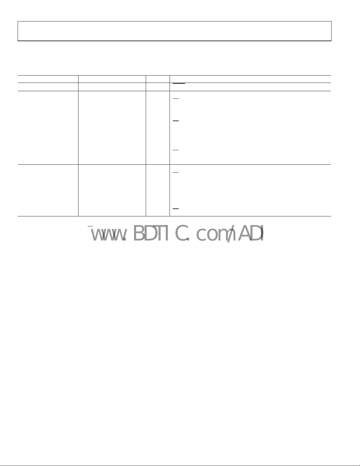
TIMING SPECIFICATIONS
All input signals are specified with 10% to 90% rise and fall times of less than 5 ns.
Table 2.
Parameter Min Typ Max Unit Test Conditions/Comments
t
1
Read Operation
t
4
1
t
SCLK falling edge to data valid delay
5
0 60 ns DVDD of 4.75 V to 5.25 V
1, 2
t
5A
0 60 ns DVDD of 4.75 V to 5.25 V
t
6
t
7
t
8
3
t
9
Write Operation
t
11
t
12
t
13
t
14
t
15
t
16
1
These numbers are measured with the load circuit shown in Figure 4 and defined as the time required for the output to cross the VOL or VOH limits.
2
This specification is relevant only if CS goes low while SCLK is low.
3
These numbers are derived from the measured time taken by the data output to change 0.5 V when loaded with the circuit shown in Figure 4. The measured number
is then extrapolated back to remove effects of charging or discharging the 50 pF capacitor. Therefore, the times quoted are the true bus relinquish times of the part
and as such are independent of external bus loading capacitances.
50 ns
0 ns
pulse width
SYNC
falling edge to SCLK falling edge setup time
CS
falling edge to data valid delay
CS
50 ns SCLK high pulse width
50 ns SCLK low pulse width
0 ns
rising edge after SCLK rising edge hold time
CS
10 80 ns Bus relinquish time after SCLK rising edge
0 ns
falling edge to SCLK falling edge setup
CS
30 ns Data valid to SCLK rising edge setup time
25 ns Data valid after SCLK rising edge hold time
50 ns SCLK high pulse width
50 ns SCLK low pulse width
0 ns
rising edge after SCLK rising edge hold time
CS
Rev. A | Page 4 of 16

ADIS16130
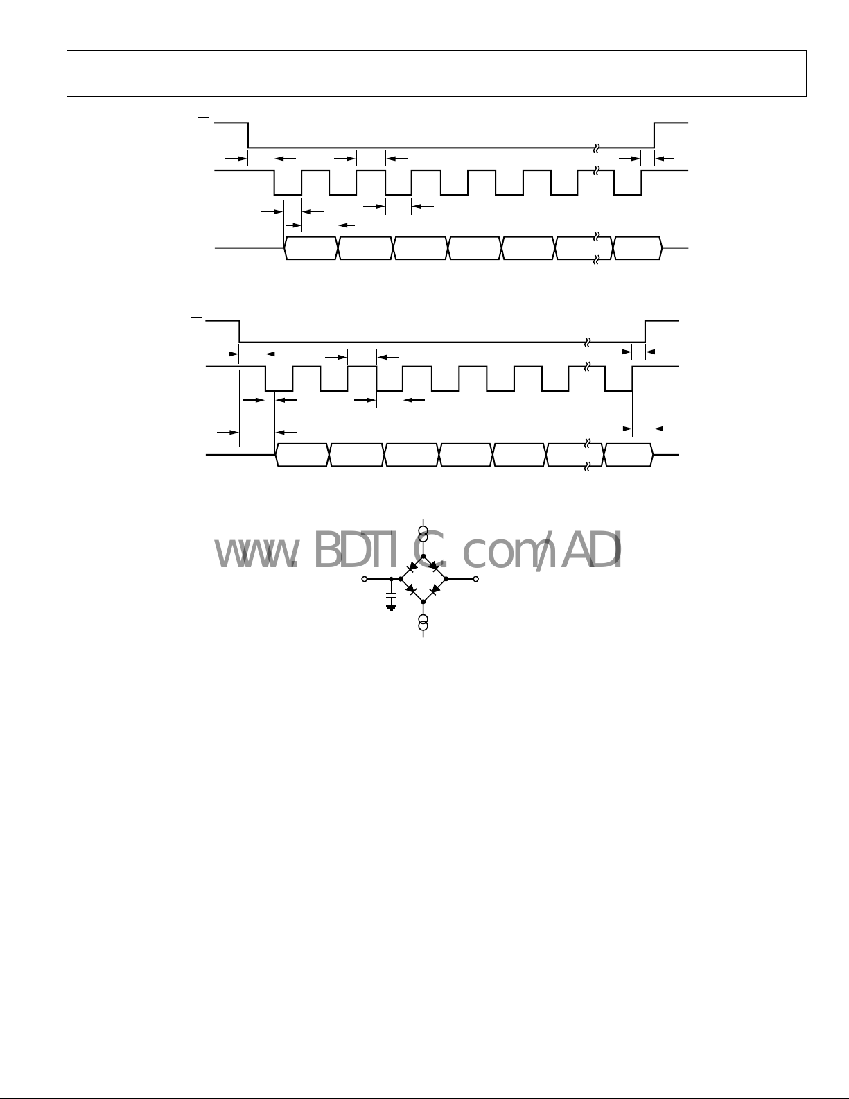
SCLK
www.BDTIC.com/ADI
CS
t
11
SCLK
t
12
t
13
SDI MSB LSB
t
14
t
15
t
16
07238-002
Figure 2. Input Timing for Write Operation
CS
t
8
t
9
07238-003
SDO
t
4
t
5
t
5A
MSB LSB
t
6
t
7
Figure 3. Output Timing for Read Operation
(800µA AT DVDD = 5V
I
SINK
100µA AT DV
DD
= 3V)
TO OUTPUT
PIN
50pF
I
SOURCE
1.6V
(200µA AT DVDD = 5V
100µA AT DV
DD
= 3V)
07328-024
Figure 4. Load Circuit for Access Time and Bus Relinquish Time
Rev. A | Page 5 of 16
 Loading...