

Dual-Axis ±5 g Accelerometer
www.BDTIC.com/ADI
FEATURES
Dual-axis accelerometer
SPI digital output interface
Internal temperature sensor
Highly integrated; minimal external components
Bandwidth externally selectable
1.9 mg resoluti
Externally controlled electrostatic self-test
3.0 V to 5.25 V single-supply operation
Low power: <2 mA
3500 g shock s
7.2 mm × 7.2 mm × 3.7 mm package
APPLICATIONS
Industrial vibration/motion sensing
Platform stabilization
Dual-axis tilt sensing
Tracking, recording, analysis devices
Alarms and security devices
on at 60 Hz
urvival
with SPI Interface
ADIS16006
GENERAL DESCRIPTION
The ADIS16006 is a low cost, low power, complete dual-axis
accelerometer with an integrated serial peripheral interface
(SPI). An integrated temperature sensor is also available on the
SPI interface. The ADIS16006 measures acceleration with a fullscale range of ±5 g (minimum). The ADIS16006 can measure both
dynamic acceleration (vibration) and static acceleration (gravity).
The typical noise floor is 200 μg/
1.9 mg (60 Hz bandwidth) to be resolved.
The bandwidth of the accelerometer is set with optional
ca
pacitors, C
and CY, at the XFILT pin and the YFILT pin.
X
Digital output data for both axes is available via the serial interface.
An externally driven self-test pin (ST) allows the user to verify
th
e accelerometer functionality.
The ADIS16006 is available in a 7.2 mm × 7.2 mm × 3.7 mm,
12-t
erminal LGA package.
√Hz, allowing signals below
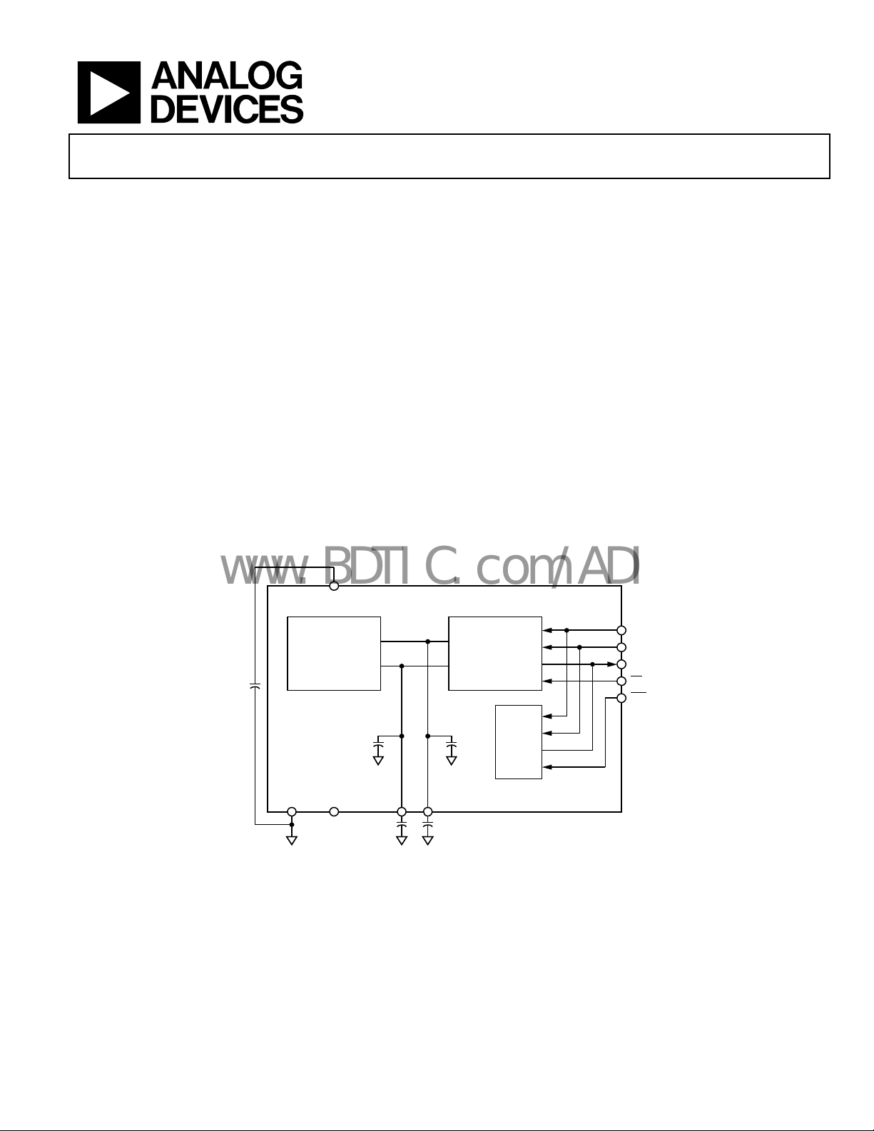
FUNCTIONAL BLOCK DIAGRAM
V
CC
ADIS16006
DUAL-AXIS
±5g
ACCELEROMETER
C
DC
COM ST
YFILT
C
XFILT
Y
Figure 1.
C
X
SERIAL
INTERFACE
TEMP
SENSOR
SCLK
DIN
DOUT
CS
TCS
05975-001
Rev. A
Information furnished by Analog Devices is believed to be accurate and reliable. However, no
responsibility is assumed by Anal og Devices for its use, nor for any infringements of patents or ot her
rights of third parties that may result from its use. Specifications subject to change without notice. No
license is granted by implication or otherwise under any patent or patent rights of Analog Devices.
Trademarks and registered trademarks are the property of their respective owners.
One Technology Way, P.O. Box 9106, Norwood, MA 02062-9106, U.S.A.
Tel: 781.329.4700 www.analog.com
Fax: 781.461.3113 ©2007 Analog Devices, Inc. All rights reserved.

ADIS16006
www.BDTIC.com/ADI
TABLE OF CONTENTS
Features .............................................................................................. 1
Applications....................................................................................... 1
General Description......................................................................... 1
Functional Block Diagram .............................................................. 1
Revision History ............................................................................... 2
Specifications..................................................................................... 3
Timing Specifications .................................................................. 4
Circuit and Timing Diagrams..................................................... 5
Absolute Maximum Ratings............................................................ 6
ESD Caution.................................................................................. 6
Pin Configuration and Function Descriptions............................. 7
Typical Performance Characteristics............................................. 8
Theory of Operation ...................................................................... 11
REVISION HISTORY
10/07—Rev. 0 to Rev. A
Changes to Features and General Description .............................1
Added Note 6 to Table 2 .................................................................. 4
Changes to Figure 5.......................................................................... 6
Changes to Accelerometer Control Register Section................. 11
Changes to Layout.......................................................................... 13
Changes to Layout.......................................................................... 14
Deleted Figure 24 and Table 11..................................................... 14
Edited Second-Level Assembly Section....................................... 15
Updated Outline Dimensions....................................................... 16
Changes to Ordering Guide.......................................................... 16
3/06—Revision 0: Initial Version
Self-Test .......................................................................................11
Serial Interface............................................................................ 11
Accelerometer Serial Interface.................................................. 11
Temperature Sensor Serial Interface........................................ 12
Power Supply Decoupling .........................................................12
Setting the Bandwidth ...............................................................13
Selecting Filter Characteristics:
The Noise/Bandwidth Trade-Off .............................................. 13
Applications..................................................................................... 15
Second Level Assembly ............................................................. 15
Outline Dimensions .......................................................................16
Ordering Guide .......................................................................... 16
Rev. A | Page 2 of 16
ADIS16006
www.BDTIC.com/ADI
SPECIFICATIONS
TA = −40°C to +125°C, VCC = 5 V, CX = CY = 0 μF, acceleration = 0 g, unless otherwise noted. All minimum and maximum specifications
are guaranteed. Typical specifications are not guaranteed.
Table 1.
Parameter Conditions Min Typ Max Unit
ACCELEROMETER SENSOR INPUT Each axis
Measurement Range
Nonlinearity % of full scale ±0.5 ±2.5 %
Package Alignment Error ±1.5 Degrees
Alignment Error X sensor to Y sensor ±0.1 Degrees
Cross-Axis Sensitivity ±1.5 ±3 %
ACCELEROMETER SENSITIVITY Each axis
Sensitivity at XFILT, YFILT 242 256 272 LSB/g
Sensitivity Change due to Temperature
ZERO g BIAS LEVEL Each axis
0 g Voltage at XFILT, YFILT 1905 2048 2190 LSB
0 g Offset vs. Temperature ±0.1 LSB/°C
ACCELEROMETER NOISE PERFORMANCE
Noise Density At 25°C 200 μg/√Hz rms
ACCELEROMETER FREQUENCY RESPONSE
CX, CY Range 0 10 μF
R
Tolerance 24 32 40 kΩ
FILT
Sensor Bandwidth CX = 0 μF, CY = 0 μF 2.26 kHz
Sensor Resonant Frequency 5.5 kHz
ACCELEROMETER SELF-TEST
Logic Input Low 0.2 × VCCV
Logic Input High 0.8 × V
ST Input Resistance to COM 30 50 kΩ
Output Change at X
TEMPERATURE SENSOR
Accuracy VCC = 3 V to 5.25 V ±2 °C
Resolution 10 Bits
Update Rate 400 μs
Temperature Conversion Time 25 μs
DIGITAL INPUT
Input High Voltage (V
V
Input Low Voltage (V
Input Current VIN = 0 V or V
Input Capacitance 10 pF
DIGITAL OUTPUT
Output High Voltage (VOH) I
Output Low Voltage (VOL) I
1
2
3, 4
5
, Y
T
OUT
OUT
) VCC = 4.75 V to 5.25 V 2.4 V
INH
) VCC = 3.0 V to 5.25 V 0.8 V
INL
±5
Delta from 25°C ±0.3 %
V
CC
Self-Test 0 to Self-Test 1 102 205 307 LSB
= 3.0 V to 3.6 V 2.1 V
CC
CC
= 200 μA, VCC = 3.0 V to 5.25 V VCC − 0.5 V
SOURCE
= 200 μA 0.4 V
SINK
−10 +1 +10 μA
Rev. A | Page 3 of 16
g

ADIS16006
www.BDTIC.com/ADI
Parameter Conditions Min Typ Max Unit
POWER SUPPLY
Operating Voltage Range 3.0 5.25 V
Quiescent Supply Current f
Power-Down Current 1.0 mA
Turn-On Time
1
Guaranteed by measurement of initial offset and sensitivity.
2
Defined as the output change from ambient-to-maximum temperature or ambient-to-minimum temperature.
3
Actual bandwidth response controlled by user-supplied external capacitor (CX, CY).
4
See the Setting the Bandwidth section for more information on how to reduce the bandwidth.
5
Self-test response changes as the square of VCC.
6
Larger values of CX and CY increase turn-on time. Turn-on time is approximately (160 × (0.0022 + CX or CY) + 4) in milliseconds, where CX and CY are in μF.
6
TIMING SPECIFICATIONS
TA = −40°C to +125°C, acceleration = 0 g, unless otherwise noted.
= 50 kSPS 1.5 1.9 mA
SCLK
CX, CY = 0.1 μF 20 ms
Table 2.
Parameter
f
SCLK
1, 2
3
VCC = 3.3 V VCC = 5 V Unit Description
10 10 kHz min
2 2 MHz max
t
CONVER T
t
ACQ
t
1
4
t
2
4
t
3
t
4
t
5
t
6
t
7
5
t
8
6
t
9
1
Guaranteed by design. All input signals are specified with tR and tF = 5 ns (10% to 90% of VCC) and timed from a voltage level of 1.6 V. The 3.3 V operating range spans
from 3.0 V to 3.6 V. The 5 V operating range spans from 4.75 V to 5.25 V.
2
See Figure 3 and Figure 4.
3
Mark/space ratio for the SCLK input is 40/60 to 60/40.
4
Measured with the load circuit in Figure 2 and defined as the time required for the output to cross 0.4 V or 2.0 V with VCC = 3.3 V and time for an output to cross 0.8 V or
2.4 V with V
5
t8 is derived from the measured time taken by the data outputs to change 0.5 V when loaded with the circuit in Figure 2. The measured number is then extrapolated
back to remove the effects of charging or discharging the 50 pF capacitor. This means that the time, t8, quoted in the Timing Specifications is the true bus relinquish
time of the part and is independent of the bus loading.
6
Shut-down recovery time denotes the time it takes to start producing samples and does not account for the recovery time of the sensor, which is dependent on the
overall bandwidth.
= 5.0 V.
CC
14.5 × t
SCLK
1.5 × t
SCLK
10 10 ns min
60 30 ns max
14.5 × t
1.5 × t
SCLK
SCLK
Throughput time = t
/CS to SCLK setup time
TCS
Delay from TCS
+ t
CONVER T
= 16 × t
ACQ
/CS until DOUT three-state disabled
100 75 ns max Data access time after SCLK falling edge
20 20 ns min Data setup time prior to SCLK rising edge
20 20 ns min Data hold time after SCLK rising edge
0.4 × t
SCLK
0.4 × t
SCLK
80 80 ns max
0.4 × t
0.4 × t
SCLK
SCLK
ns min SCLK high pulse width
ns min SCLK low pulse width
/CS rising edge to DOUT high impedance
TCS
5 5 μs typ Power-up time from shutdown
SCLK
Rev. A | Page 4 of 16
ADIS16006
www.BDTIC.com/ADI
CIRCUIT AND TIMING DIAGRAMS
200µA I
TO OUTPUT
PIN
C
L
50pF
200µA I
Figure 2. Load Circuit for Digital Out
OL
1.6V
OH
05975-002
put Timing Specifications
t
ACQ
CS
t
1
SCLK
THREE-STATE THREE-STATE
DOUT
DIN
1
t
2
t
4
t
5
DON’T
CARE
t
6
234
t
7
4 LEADING Z E ROS
ZERO ZERO ZERO ADD0 ONE ZERO PM0
56 15
Figure 3. Accelerometer Serial Interface Timing Diagram
t
3
DB11
t
CONVERT
DB10
16
DB9 DB0
t
8
5975-003
TCS
t
1
SCLK
THREESTATE THREE-STATE
DOUT
1
LEADING
ZERO
t
6
234
t
3
t
7
DB9 DB8
11 15
DB0
16
t
8
DIN
5975-004
Figure 4. Temperature Serial Interface Timing Diagram
Rev. A | Page 5 of 16

ADIS16006
www.BDTIC.com/ADI
ABSOLUTE MAXIMUM RATINGS
Table 3.
Parameter Rating
Acceleration (Any Axis, Unpowered) 3500 g
Acceleration (Any Axis, Powered) 3500 g
V
CC
−0.3 V to +7.0 V
All Other Pins (COM − 0.3 V) to (VCC + 0.3 V)
Output Short-Circuit Duration
Indefinite
(Any Pin to Common)
Operating Temperature Range −40°C to +125°C
Storage Temperature Range −65°C to +150°C
Stresses above those listed under Absolute Maximum Ratings
may cause permanent damage to the device. This is a stress
rating only; functional operation of the device at these or any
other conditions above those indicated in the operational
section of this specification is not implied. Exposure to absolute
maximum rating conditions for extended periods may affect
device reliability.
Table 4. Package Characteristics
Package Type θ
JA
θ
JC
Device Weight
12-Terminal LGA 200°C/W 25°C/W 0.3 grams
3.1865
1.797
8×
3.594
6.373
4×
2×
1.127
12×
7.2mm × 7.2mm S TACKED LGA. ALL DIMENSIONS IN mm.
Figure 5. Second-Level Assembly Pad Layout
8×
0.670
8×
0.500
12×
05975-005
ESD CAUTION
Rev. A | Page 6 of 16

ADIS16006
K
www.BDTIC.com/ADI
PIN CONFIGURATION AND FUNCTION DESCRIPTIONS
CC
V
ADIS16006
TOP VIEW
(Not to S cale)
NC
CS
1012 11
9
XFILT
82
YFILT
7
NC
65
ST
05975-006
1
TCS
DOUT
3
DIN
NC = NO CONNECT
SCL
4
COM
Figure 6. Pin Configuration
Table 5. Pin Function Descriptions
Pin No. Mnemonic Description
1
TCS
Temperature Chip Select. Active low logic input. This input frames the serial data transfer for the temperature
sensor output.
2 DOUT
Data Out, Logic Output. The conversion of the ADIS16006 is pr
ovided on this output as a serial data stream.
The bits are clocked out on the falling edge of the SCLK input.
3 DIN
Data In, Logic Input. Data to be written into the control r
egister of the ADIS16006 is provided on this input and
is clocked into the register on the rising edge of SCLK.
4 COM Common. Reference point for all circuitry on the ADIS16006.
5, 7 NC No Connect.
6 ST Self-Test Input. Active high logic input. Simulates a nominal 0.75 g test input for diagnostic purpose.
8 YFILT
Y-Channel Filter Node. Used in conjunction with an optiona
l external capacitor to band limit the noise
contribution from the accelerometer.
9 XFILT
X-Channel Filter Node. Used in conjunction with an optiona
l external capacitor to band limit the noise
contribution from the accelerometer.
10
CS
Chip Select. Active low logic input. This input provides the dual function of initiating the accelerometer
conversions on the ADIS16006 and framing the serial data transfer for the accelerometer output.
11 V
CC
12 SCLK
Power Supply Input. The VCC range for the ADIS16006 is 3.0 V to 5.25 V.
Serial Clock, Logic Input. SCLK provides the serial clock for ac
cessing data from the part and writing serial data to
the control register. This clock input is also used as the clock source for the conversion process of the ADIS16006.
Rev. A | Page 7 of 16

ADIS16006
www.BDTIC.com/ADI
TYPICAL PERFORMANCE CHARACTERISTICS
25
262
261
260
259
258
257
SENSITIVITY (LSB/g)
256
255
254
–50 –25 0 25 50 75 100 125 150
TEMPERATURE (° C)
Figure 7. Sensitivity vs. Temperature (±1 g Stimulus)
2048
2046
2044
AVG AT 3.60V
5.25V
AVG AT 5.25V
AVG AT 4.75V
B3-Y
B3-X
B1-Y
B5-X
B2-X
B1-X
B5-Y
B4-X
B2-Y
B4-Y
05975-007
AVERAGE = 2040. 6 6
STANDARD DEVIAT ION = 23.19
20
15
10
5
PERCENT OF POPULATION (%)
0
1995
2000
2005
2010
Figure 10. X-Axis 0 g B
40
AVERAGE = 2055. 8 75
STANDARD DEVIAT ION = 6.464
35
30
25
20
2015
2020
2025
2030
2035
2040
2045
OUTPUT (LSB)
ias at 25°C
2050
2055
2060
2065
2070
2075
2080
2085
2090
05975-010
2042
BIAS LEVEL (L SB)
2040
2038
–40 –20 0 20 40 60 80 100 120
TEMPERATURE (°C)
Figure 8. X-Axis 0 g
AVG AT 3.00V
Bias vs. Temperature
2048
2047
2046
2045
2044
2043
2042
BIAS LEVEL (L S B)
2041
2040
2039
2038
3.0 5.55.04.54.03.5
Figure 9. X-Axis 0 g
+125°C
+25°C
–40°C
VCC (V)
Bias vs. Supply Voltage
AVG AT 3. 30V
15
10
PERCENT OF POPULATION (%)
5
0
1995
2000
2005
2010
2015
2020
2025
2030
2035
2040
2045
2050
2055
2060
2065
2070
2075
2080
2085
05975-008
Figure 11. Y-Axis 0 g B
OUTPUT (LSB)
ias at 25°C
2090
05975-011
60
50
40
30
20
PERCENT OF POPULATION (%)
10
0
80 85 90 95 100 105 110 115 120 125 130 135 140
05975-009
Figure 12. Noise (X-Axis) at V
NOISE (µg/ Hz)
= 5 V, 25°C
CC
05975-012
Rev. A | Page 8 of 16

ADIS16006
www.BDTIC.com/ADI
45
40
35
30
25
20
15
10
PERCENT OF POPULATION (%)
5
0
80 85 90 95 100 105 110 115 120 125 130 135 140
Figure 13. Noise (Y-Axis) at V
NOISE (µg/ Hz)
= 5 V, 25°C
CC
40
AVERAGE = 202. 21 37
STANDARD DEVIATION = 12.09035
35
30
25
20
15
10
PERCENT OF POPULATION (%)
5
0
110 130 150 170 190 210 230 250 270 290
Figure 14. X-Axis Self-Test at V
OUTPUT (LSB)
= 5 V, 25°C
CC
40
AVERAGE = 82.8928 1
STANDARD DEVIATION = 4. 9080 12
35
30
25
20
15
10
PERCENT OF POPULATION (%)
5
0
OUTPUT (LSB)
Figure 15. X-Axis Self-Test at V
= 3.3 V, 25°C
CC
05975-013
05975-014
110105100959085807570656055504540
05975-015
250
200
150
100
SELF TEST (L SB)
50
0
AVG AT 5.25V
AVG AT 5.00V
AVG AT 4.75V
AVG AT 3.60V
AVG AT 3.30V
AVG AT 3.00V
TEMPERATURE (° C)
15050 1000–50
05975-016
Figure 16. Self-Test X-Axis vs. Temperature
250
230
210
190
170
150
130
SELF TEST (LSB)
110
90
70
50
4.0 4.5 5.03.53.0
VCC (V)
+125°C
–40°C
+25°C
5.5
05975-017
Figure 17. Self-Test X-Axis vs. Supply Voltage
1.8
1.7
1.6
1.5
1.4
1.3
SUPPLY CURRENT (mA)
1.2
1.1
1.0
VCC (V)
+125°C
+25°C
–40°C
5.54.0 4.5 5.03.53.0
05975-018
Figure 18. Supply Current vs. Supply Voltage
Rev. A | Page 9 of 16

ADIS16006
www.BDTIC.com/ADI
45
35
25
15
5
PERCENT OF POPULATION (%)
–5
VCC = 5.0V
VCC = 3.3V
CURRENT (mA)
1.591.15 1.19 1.23 1.27 1.31 1.35 1.39 1.43 1.47 1.51 1.55
05975-023
Figure 19. Supply Current at 25°C
60
50
40
VCC = 5.0V
VCC = 3.3V
1.3
1.2
1.1
+125°C
1.0
0.9
0.8
0.7
POWER-DO W N SUPPLY CURRENT ( mA)
0.6
+25°C
–40°C
VCC (V)
Figure 21. Power-Down Supply Current vs. Supply Voltage
0.6
0.4
0.2
0
5.55.04.54.03.53.0
05975-020
30
20
PERCENT OF POPULATION (%)
10
0
CURRENT (mA)
1.100.70 0.74 0.78 0.82 0.86 0.90 0.94 0.98 1.02 1.06
05975-019
Figure 20. Power-Down Supply Current
–0.2
–0.4
SAMPLING ERROR (dB)
–0.6
–0.8
–1.0
SAMPLE RATE (kSPS)
Figure 22. Sampling Error vs. Sampling Frequency
100110
05975-024
Rev. A | Page 10 of 16

ADIS16006
www.BDTIC.com/ADI
THEORY OF OPERATION
The ADIS16006 is a low cost, low power, complete dual-axis
accelerometer with an integrated serial peripheral interface
(SPI) and an integrated temperature sensor whose output is
also available on the SPI interface. The ADIS16006 is capable of
measuring acceleration with a full-scale range of ±5 g (minimum).
The ADIS16006 can measure both dynamic acceleration
(vibration) and static acceleration (gravity).
SELF-TEST
The ST pin controls the self-test feature. When this pin is set to
, an electrostatic force is exerted on the beam of the acceler-
V
CC
ometer. The resulting movement of the beam allows the user to
test if the accelerometer is functional. The typical change in
output is 801 mg (corresponding to 205 LSB) for V
This pin can be left open-circuit or connected to common in
normal use. The ST pin should never be exposed to voltage
greater than V
condition cannot be guaranteed (for example, multiple supply
voltages are present), a low V
V
is recommended.
CC
+ 0.3 V. If the system design is such that this
CC
clamping diode between ST and
F
= 5.0 V.
CC
SERIAL INTERFACE
The serial interface on the ADIS16006 consists of five wires: CS,
TCS
, SCLK, DIN, and DOUT. Both accelerometer axes and the
temperature sensor data are available on the serial interface.
TCS
CS
The
and
perature sensor outputs, respectively.
active at the same time.
The SCLK input accesses data from the internal data registers.
are used to select the accelerometer or tem-
CS
TCS
and
cannot be
ACCELEROMETER SERIAL INTERFACE
Figure 3 shows the detailed timing diagram for serial interfacing to
the accelerometer in the ADIS16006. The serial clock provides
the conversion clock.
data transfer and also frames the serial data transfer for the
accelerometer output. The accelerometer output is sampled on
the second rising edge of the SCLK input after the falling edge
CS
of
. The conversion requires 16 SCLK cycles to complete. The
rising edge of
low, the next digital conversion is initiated. The details for the
control register bit functions are shown in Tabl e 6.
CS
CS
initiates the conversion process and
puts the bus back into three-state. If CS remains
Accelerometer Control Register
MSB LSB
DONTC ZERO ZERO ZERO ADD0 ONE ZERO PM0
Table 6. Accelerometer Control Register Bit Functions
Bit Mnemonic Comments
7 DONTC Don’t care. Can be 1 or 0.
6, 5, 4 ZERO These bits should be held low.
3 ADD0
2 ONE This bit should be held high.
1 ZERO This bit should be held low.
0 PM0
This address bit selects the x-axis or y-axis
. A 0 selects the x-axis; a 1 selects
outputs
the y-axis.
This bit selects the operation mode for
celerometer; set to 0 for normal
the ac
operation and 1 for power-down mode.
Power-Down
By setting PM0 to 1 when updating the accelerometer
control register, the ADIS16006 goes into shutdown mode.
The information stored in the control register is maintained
during shutdown. The ADIS16006 changes modes as soon as the
control register is updated. If the part is in shutdown mode and
PM0 is changed to 0, the part powers up on the 16th SCLK
rising edge.
ADD0
By setting ADD0 to 0 when updating the accelerometer control
register, the x-axis output is selected. By setting ADD0 to 1, the
y-axis output is selected.
ZERO
ZERO is defined as the Logic low level.
ONE
ONE is defined as the Logic high level.
DONTC
DONTC is defined as don’t care and can be a low or high
logic level.
Accelerometer Conversion Details
Every time the accelerometer is sampled, the sampling function
discharges the internal C
of their initial values (assuming no additional external filtering
capacitors are added). The recovery time for the filter capacitor
to recharge is approximately 10 μs. Therefore, sampling the
accelerometer at a rate of 10 kSPS or less does not induce a
sampling error. However, as sampling frequencies increase
above 10 kSPS, one can expect sampling errors to attenuate
the actual acceleration levels.
or CY filtering capacitors by up to 2%
X
Rev. A | Page 11 of 16

ADIS16006
www.BDTIC.com/ADI
TEMPERATURE SENSOR SERIAL INTERFACE
Read Operation
Figure 4 shows the timing diagram for a serial read from the
TCS
temperature sensor. The
Ten bits of data and a leading zero are transferred during a read
operation. Read operations occur during streams of 16 clock
pulses. The serial data can be received into two bytes to
accommodate the entire 10-bit data stream. If only eight bits
of resolution are required, the data can be received into a single
byte. At the end of the read operation, the DOUT line remains
in the state of the last bit of data clocked out until
high, at which time the DOUT line from the temperature
sensor goes three-state.
Write Operation
Figure 4 also shows the timing diagram for the serial write
to the temperature sensor. The write operation takes place at
the same time as the read operation. Data is clocked into the
control register on the rising edge of SCLK. DIN should remain
low for the entire cycle.
Temperature Sensor Control Register
MSB LSB
ZERO ZERO ZERO ZERO ZERO ZERO ZERO ZERO
Table 7. Temperature Sensor Control Register Bit Functions
Bit Mnemonic Comments
7 to 0 ZERO All bits should be held low.
ZERO
ZERO is defined as the Logic low level.
Output Data Format
The output data format for the temperature sensor is twos
complement. Tabl e 8 shows the relationship between the
emperature and the digital output.
t
Table 8. Temperature Sensor Data Format
Temperature Digital Output (DB9 … DB0)
−40°C 11 0110 0000
−25°C 11 1001 1100
−0.25°C 11 1111 1111
0°C 00 0000 0000
+0.25°C 00 0000 0001
+10°C 00 0010 1000
+25°C 00 0110 0100
+50°C 00 1100 1000
+75°C 01 0010 1100
+100°C 01 1001 0000
+125°C 01 1111 0100
line enables the SCLK input.
TCS
goes
Temperature Sensor Conversion Details
The ADIS16006 features a 10-bit digital temperature sensor that
allows an accurate measurement of the ambient device temperature
to be made.
The conversion clock for the temperature sensor is internally
enerated; therefore, no external clock is required except when
g
reading from and writing to the serial port. In normal mode, an
internal clock oscillator runs the automatic conversion sequence. A
conversion is initiated approximately every 350 μs. At this time,
the temperature sensor wakes up and performs a temperature
conversion. This temperature conversion typically takes 25 μs,
at which time the temperature sensor automatically shuts down.
The result of the most recent temperature conversion is available in the serial output register at any time. Once the conversion is
finished, an internal oscillator starts counting and is designed to
time out every 350 μs. The temperature sensor then powers up
and does a conversion.
TCS
If the
temperature value is output onto the DOUT line every time
without changing. It is recommended that the
be brought low every 350 μs (±30%) or less. The ±30% covers
process variation. The
outside this range.
The device is designed to autoconvert every 350 μs. If the
t
emperature sensor is accessed during the conversion process,
an internal signal is generated to prevent any update of the
temperature value register during the conversion. This prevents
the user from reading back spurious data. The design of this
feature results in this internal lockout signal being reset only at
the start of the next autoconversion. Therefore, if the
goes active before the internal lockout signal is reset to its inactive
mode, the internal lockout signal is not reset. To ensure that no
lockout signal is set, bring
(±30%). As a result, the temperature sensor is not interrupted
during a conversion process.
In the automatic conversion mode, every time a read or write
o
peration takes place, the internal clock oscillator is restarted at
the end of the read or write operation. The result of the conversion
is typically available 25 μs later. Reading from the device before
conversion is complete provides the same set of data.
is brought low every 350 μs (±30%) or less, the same
TCS
line not
TCS
should become active (high to low)
TCS
line
TCS
low at a greater time than 350 μs
POWER SUPPLY DECOUPLING
The ADIS16006 integrates two decoupling capacitors that are
0.047 μF in value. For local operation of the ADIS16006, no
additional power supply decoupling capacitance is required.
However, if the system power supply presents a substantial
amount of noise, additional filtering can be required. If additional
capacitors are required, connect the ground terminal of each
of these capacitors directly to the underlying ground plane.
Finally, note that all analog and digital grounds should be
referenced to the same system ground reference point.
Rev. A | Page 12 of 16

ADIS16006
www.BDTIC.com/ADI
SETTING THE BANDWIDTH
The ADIS16006 has provisions for band limiting the accelerometer. Capacitors can be added at the XFILT pin and the
YFILT pin to implement further low-pass filtering for
antialiasing and noise reduction. The equation for the 3 dB
bandwidth is
= 1/(2π(32 kΩ) × (C
f
−3dB
(XFILT, YFILT)
or more simply,
f
= 5 μF/(C
−3dB
(XFILT, YFILT)
+ 2200 pF)
The tolerance of the internal resistor (R
much as ±25% of its nominal value (32 kΩ); thus, the bandwidth
varies accordingly.
A minimum capacitance of 0 pF for C
Table 9. Filter Capacitor Selection, C
Bandwidth (Hz) Capacitor (μF)
1 4.7
10 0.47
50 0.10
100 0.047
200 0.022
400 0.01
2250 0
+ 2200 pF))
) can vary typically as
FILT
XFILT
and C
XFILT
YFILT
and C
is allowable.
YFILT
SELECTING FILTER CHARACTERISTICS: THE NOISE/BANDWIDTH TRADE-OFF
The accelerometer bandwidth selected ultimately determines
the measurement resolution (smallest detectable acceleration).
Filtering can be used to lower the noise floor, which improves
the resolution of the accelerometer. Resolution is dependent on
the analog filter bandwidth at XFILT and YFILT.
The ADIS16006 has a typical bandwidth of 2.25 kHz with no
ext
ernal filtering. The analog bandwidth can be further
decreased to reduce noise and improve resolution.
The ADIS16006 noise has the characteristics of white Gaussian
oise, which contributes equally at all frequencies and is described
n
in terms of μg/√Hz (that is, the noise is proportional to the
square root of the bandwidth of the accelerometer). The user
should limit bandwidth to the lowest frequency needed by the
application to maximize the resolution and dynamic range of
the accelerometer.
With the single-pole, roll-off characteristic, the typical noise of
e ADIS16006 is determined by
th
rmsNoise = (200 μ
At 100 Hz, the noise is
rmsNoise = (200 μ
Often, the peak value of the noise is desired. Peak-to-peak noise
ca
n only be estimated by statistical methods.
fo
r estimating the probabilities of exceeding various peak
values, given the rms value.
g/√Hz) × (√(BW × 1.57))
g/√Hz) × (√(100 × 1.57)) = 2.5 mg
Table 1 0 is useful
Table 10. Estimation of Peak-to-Peak Noise
Percentage of Time Noise Exceeds
Peak-to-Peak Value
2 × rms 32
4 × rms 4.6
6 × rms 0.27
8 × rms 0.006
Nominal P
eak-to-Peak Value (%)
Rev. A | Page 13 of 16

ADIS16006
www.BDTIC.com/ADI
12
DIGITAL OUTPUT (IN LSBs)
X-AXIS: 1792
Y-AXIS: 2048
3 2 1
1011
8 97
89 7
1011
DIGITAL OUTPUT (IN LSBs)
X-AXIS: 2048
Y-AXIS: 2304
12
4
65
Top View
Not to Scale
4
321
6 5
DIGITAL OUTPUT (IN LSBs)
89 7
X-AXIS: 23 04
Y-AXIS: 20 48
10 11
Figure 23. Output Respons
65
4
65
4
321
12
e vs. Orientation
3 2 1
DIGITAL OUTPUT ( IN LSBs)
X-AXIS: 2048
Y-AXIS: 1792
8 97
DIGITAL OUTPUT (IN LSBs)
X-AXIS: 2 048
Y-AXIS: 2 048
12
11
10
05975-021
Rev. A | Page 14 of 16

ADIS16006
www.BDTIC.com/ADI
APPLICATIONS
SECOND LEVEL ASSEMBLY
The ADIS16006 can be attached to the second level assembly
board using SN63 (or equivalent) or lead-free solder. IPC/
JEDEC J-STD-020 and J-STD-033 provide standard handling
procedures for these types of packages.
Rev. A | Page 15 of 16

ADIS16006
www.BDTIC.com/ADI
OUTLINE DIMENSIONS
3.594
BSC
7.35
MAX
7.20
TYP
6 .373
BSC
(2×)
1.797
BSC
(8×)
9
(4×)
10 12
1
PIN 1
INDICATOR
1.00 BSC
(12×)
TOP VIEW
5.00
TYP
SIDE VIEW
3.70
MAX
0.200
MIN
(ALL SIDES)
7
BOTTOM VIEW
3
46
0.797 BSC
(8×)
0.373 BSC
(12×)
092407-C
Figure 24. 12-Terminal Land Grid Array [LGA]
(CC-12-1)
Dim
ensions shown in millimeters
ORDERING GUIDE
Model Temperature Range Package Description Package Option
ADIS16006CCCZ
ADIS16006/PCBZ
1
Z = RoHS Compliant Part.
1
1
−40°C to +125°C 12-Terminal Land Grid Array (LGA) CC-12-1
Evaluation Board
©2007 Analog Devices, Inc. All rights reserved. Trademarks and
registered trademarks are the property of their respective owners.
D05975-0-10/07(A)
Rev. A | Page 16 of 16
 Loading...