Dual-Axis ±1.7 g Accelerometer
T
C
Data Sheet
FEATURES
Dual-axis accelerometer
SPI digital output interface
Internal temperature sensor
Highly integrated; minimal external components
Bandwidth externally selectable
1 mg resolution at 60 Hz
Externally controlled electrostatic self-test
3.0 V to 5.25 V single-supply operation
Low power: <2 mA
3500 g shock survival
7.2 mm × 7.2 mm × 3.7 mm package
APPLICATIONS
Industrial vibration/motion sensing
Platform stabilization
Dual-axis tilt sensing
Tracking, recording, and analysis devices
Alarms and security devices
with SPI Interface
ADIS16003
GENERAL DESCRIPTION
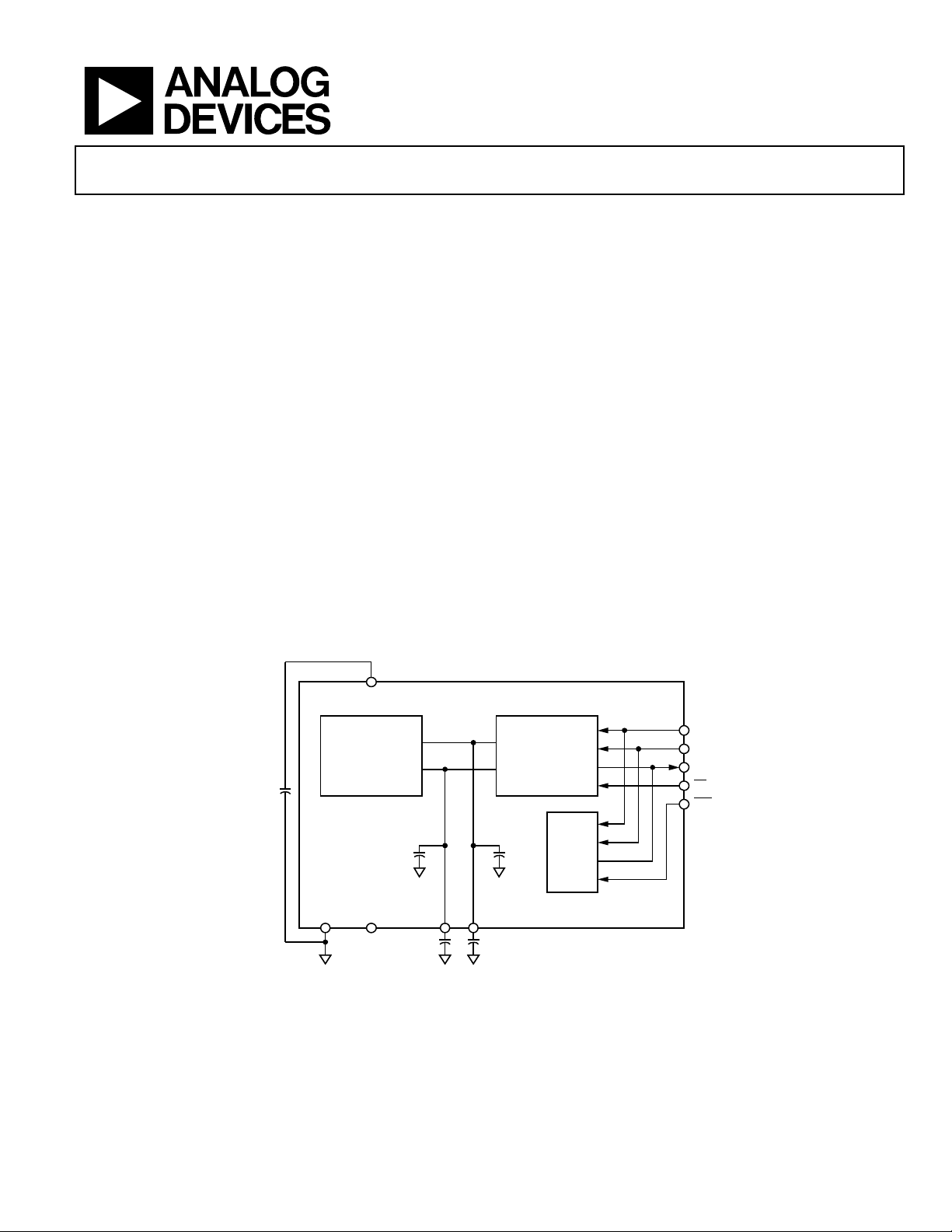
The ADIS16003 is a low cost, low power, complete dual-axis
accelerometer with an integrated serial peripheral interface
(SPI). An integrated temperature sensor is also available on the
SPI interface. The ADIS16003 measures acceleration with a fullscale range of ±1.7 g (minimum), and it can measure both dynamic
acceleration (vibration) and static acceleration (gravity).
The typical noise floor is 110 μg/√Hz, allowing signals below
1 mg (60 Hz bandwidth) to be resolved.
The bandwidth of the accelerometer is set with optional capacitors C
and CY at the XFILT and YFILT pins. Selection of the
X
two analog input channels is controlled via the serial interface.
An externally driven self-test pin (ST) allows the user to verify
the accelerometer functionality.
The ADIS16003 is available in a 7.2 mm × 7.2 mm × 3.7 mm,
12-terminal LGA package.
FUNCTIONAL BLOCK DIAGRAM
V
CC
DUAL-AXIS
±1.7g
ACCELEROMETER
DC
COM ST
YFILT
C
XFILT
Y
Figure 1.
C
X
SERIAL
INTERFACE
TEMP
SENSOR
SCLK
DIN
DOU
CS
TCS
056463-001
Rev. B
Information furnished by Analog Devices is believed to be accurate and reliable. However, no
responsibility is assumed by Anal og Devices for its use, nor for any infringements of patents or ot her
rights of third parties that may result from its use. Specifications subject to change without notice. No
license is granted by implication or otherwise under any patent or patent rights of Analog Devices.
Trademarks and registered trademarks are the property of their respective owners.
One Technology Way, P.O. Box 9106, Norwood, MA 02062-9106, U.S.A.
Tel: 781.329.4700 www.analog.com
Fax: 781.461.3113 ©2005-2012 Analog Devices, Inc. All rights reserved.

ADIS16003 Data Sheet
TABLE OF CONTENTS
Features.............................................................................................. 1
Applications....................................................................................... 1
General Description......................................................................... 1
Functional Block Diagram ..............................................................1
Revision History ...............................................................................2
Specifications..................................................................................... 3
Timing Specifications ..................................................................4
Circuit and Timing Diagrams..................................................... 5
Absolute Maximum Ratings............................................................ 6
ESD Caution.................................................................................. 6
Pin Configuration and Function Descriptions............................. 7
Typical Performance Characteristics............................................. 8
Theory of Operation ......................................................................11
Accelerometer Data Format...................................................... 11
REVISION HISTORY
3/12—Rev. A to Rev. B
Added Accelerometer Data Format Section and Table 6;
Renumbered Sequentially.............................................................. 11
10/07—Rev. 0 to Rev. A
Changes to Features and General Description .............................1
Added Note 6 to Table 2 .................................................................. 4
Changes to Figure 5.......................................................................... 6
Changes to Serial Interface Section and Layout......................... 11
Changes to Layout.......................................................................... 14
Deleted Figure 24 and Table 11..................................................... 14
Changes to Converting Acceleration to Tilt Section and
Second-Level Assembly Section ...................................................15
Updated Outline Dimensions....................................................... 16
Changes to Ordering Guide.......................................................... 16
10/05—Revision 0: Initial Version
Self-Test ....................................................................................... 11
Serial Interface............................................................................ 11
Accelerometer Serial Interface.................................................. 11
Temperature Sensor Serial Interface........................................ 12
Power Supply Decoupling......................................................... 12
Setting the Bandwidth ............................................................... 13
Selecting Filter Characteristics: The Noise/Bandwidth Trade-
Off................................................................................................. 13
Applications Information.............................................................. 15
Dual-Axis Tilt Sensor ................................................................15
Second Level Assembly ............................................................. 15
Outline Dimensions....................................................................... 16
Ordering Guide .......................................................................... 16
Rev. B | Page 2 of 16

Data Sheet ADIS16003
SPECIFICATIONS
TA = –40°C to +125°C, VCC = 5 V, CX, CY = 0 μF, acceleration = 0 g, unless otherwise noted. All minimum and maximum specifications are
guaranteed. Typical specifications are not guaranteed.
Table 1.
Parameter Conditions Min Typ Max Unit
ACCELEROMETER SENSOR INPUT Each axis
Measurement Range1 ±1.7
Nonlinearity % of full scale ±0.5 ±2.5 %
Package Alignment Error ±1.5 Degrees
Alignment Error X sensor to Y sensor ±0.1 Degrees
Cross-Axis Sensitivity ±2 ±5 %
ACCELEROMETER SENSITIVITY Each axis
Sensitivity at XFILT, YFILT 769 820 885 LSB/g
Sensitivity Change due to Temperature2 Delta from 25°C ±8 LSB
ZERO g BIAS LEVEL Each axis
0 g Voltage at XFILT, YFILT 1905 2048 2190 LSB
0 g Offset vs. Temperature ±0.14 LSB/°C
ACCELEROMETER NOISE PERFORMANCE
Noise Density At 25°C 110 μg/√Hz rms
ACCELEROMETER FREQUENCY RESPONSE3
CX, CY Range4 0 10 μF
R
Tolerance 24 32 40 kΩ
FILT
Sensor Resonant Frequency 5.5 kHz
ACCELEROMETER SELF-TEST
Logic Input Low 0.2 × VCC V
Logic Input High 0.8 × VCC V
ST Input Resistance to COM 30 50 kΩ
Output Change at X
OUT
5
, Y
Self-Test 0 to Self-Test 1 323 614 904 LSB
OUT
TEMPERATURE SENSOR
Accuracy VCC = 3 V to 5.25 V ±2 °C
Resolution 10 Bits
Update Rate 400 μs
Temperature Conversion Time 25 μs
DIGITAL INPUT
Input High Voltage (V
V
Input Low Voltage (V
) VCC = 4.75 V to 5.25 V 2.4 V
INH
= 3.0 V to 3.6 V 2.1 V
CC
) VCC = 3.0 V to 5.25 V 0.8 V
INL
Input Current VIN = 0 V or VCC −10 +1 +10 μA
Input Capacitance 10 pF
DIGITAL OUTPUT
Output High Voltage (VOH) I
Output Low Voltage (VOL) I
= 200 μA, VCC = 3.0 V to 5.25 V VCC − 0.5 V
SOURCE
= 200 μA 0.4 V
SINK
POWER SUPPLY
Operating Voltage Range 3.0 5.25 V
Quiescent Supply Current f
= 50 kSPS 1.5 2.0 mA
SCLK
Power-Down Current 1.0 mA
Turn-On Time6 C
1
Guaranteed by measurement of initial offset and sensitivity.
2
Defined as the output change from ambient-to-maximum temperature or ambient-to-minimum temperature.
3
Actual bandwidth response controlled by user-supplied external capacitor (CX, CY).
4
Bandwidth = 1/(2π × 32 kΩ × (2200 pF + C)). For CX, CY = 0 μF, bandwidth = 2260 Hz. For CX, CY = 10 μF, bandwidth = 0.5 Hz. Minimum/maximum values not tested.
5
Self-test response changes as the square of VCC.
6
Larger values of CX, CY increase turn-on time. Turn-on time is approximately 160 × (0.0022 μF + Cx + Cy) + 4 ms, where CX, CY are in μF.
, CY = 0.1 μF 20 ms
X
Rev. B | Page 3 of 16
g

ADIS16003 Data Sheet
TIMING SPECIFICATIONS
TA = −40°C to +125°C, acceleration = 0 g, unless otherwise noted.
Table 2.
Parameter
f
SCLK
1, 2
3
V
10 10 kHz min
= 3.3 V VCC = 5 V Unit Description
CC
2 2 MHz max
t
14.5 × t
CONVER T
t
1.5 × t
ACQ
t1 10 10 ns min
4
t
60 30 ns max
2
4
t
100 75 ns max Data access time after SCLK falling edge
3
14.5 × t
SCLK
1.5 × t
SCLK
SCLK
Throughput time = t
SCLK
/CS to SCLK setup time
TCS
Delay from TCS
+ t
CONVER T
ACQ
= 16 t
SCLK
/CS until DOUT three-state disabled
t4 20 20 ns min Data setup time prior to SCLK rising edge
t5 20 20 ns min Data hold time after SCLK rising edge
t6 0.4 × t
t7 0.4 × t
5
t
80 80 ns max
8
6
t
5 5 μs typ Power-up time from shutdown
9
1
Guaranteed by design. All input signals are specified with tr and tf = 5 ns (10% to 90% of VCC) and timed from a voltage level of 1.6 V. The 3.3 V operating range spans
from 3.0 V to 3.6 V. The 5 V operating range spans from 4.75 V to 5.25 V.
2
See Figure 3 and Figure 4.
3
Mark/space ratio for the SCLK input is 40/60 to 60/40.
4
Measured with the load circuit in Figure 2 and defined as the time required for the output to cross 0.4 V or 2.0 V with V
2.4 V with V
5
t8 is derived from the measured time taken by the data outputs to change 0.5 V when loaded with the circuit in Figure 2. The measured number is then extrapolated
back to remove the effects of charging or discharging the 50 pF capacitor. This means that the time, t8, quoted in the timing characteristics is the true bus relinquish
time of the part and is independent of the bus loading.
6
Shut-down recovery time denotes the time it takes to start producing samples and does not account for the recovery time of the sensor, which is dependent on the
overall bandwidth.
= 5.0 V.
CC
0.4 × t
SCLK
0.4 × t
SCLK
ns min SCLK high pulse width
SCLK
ns min SCLK low pulse width
SCLK
/CS rising edge to DOUT high impedance
TCS
= 3.3 V and time for an output to cross 0.8 V or
CC
Rev. B | Page 4 of 16

Data Sheet ADIS16003
T
CIRCUIT AND TIMING DIAGRAMS
O OUTPUT
PIN
50pF
C
200µA I
L
200µA I
OL
1.6V
OH
05463-002
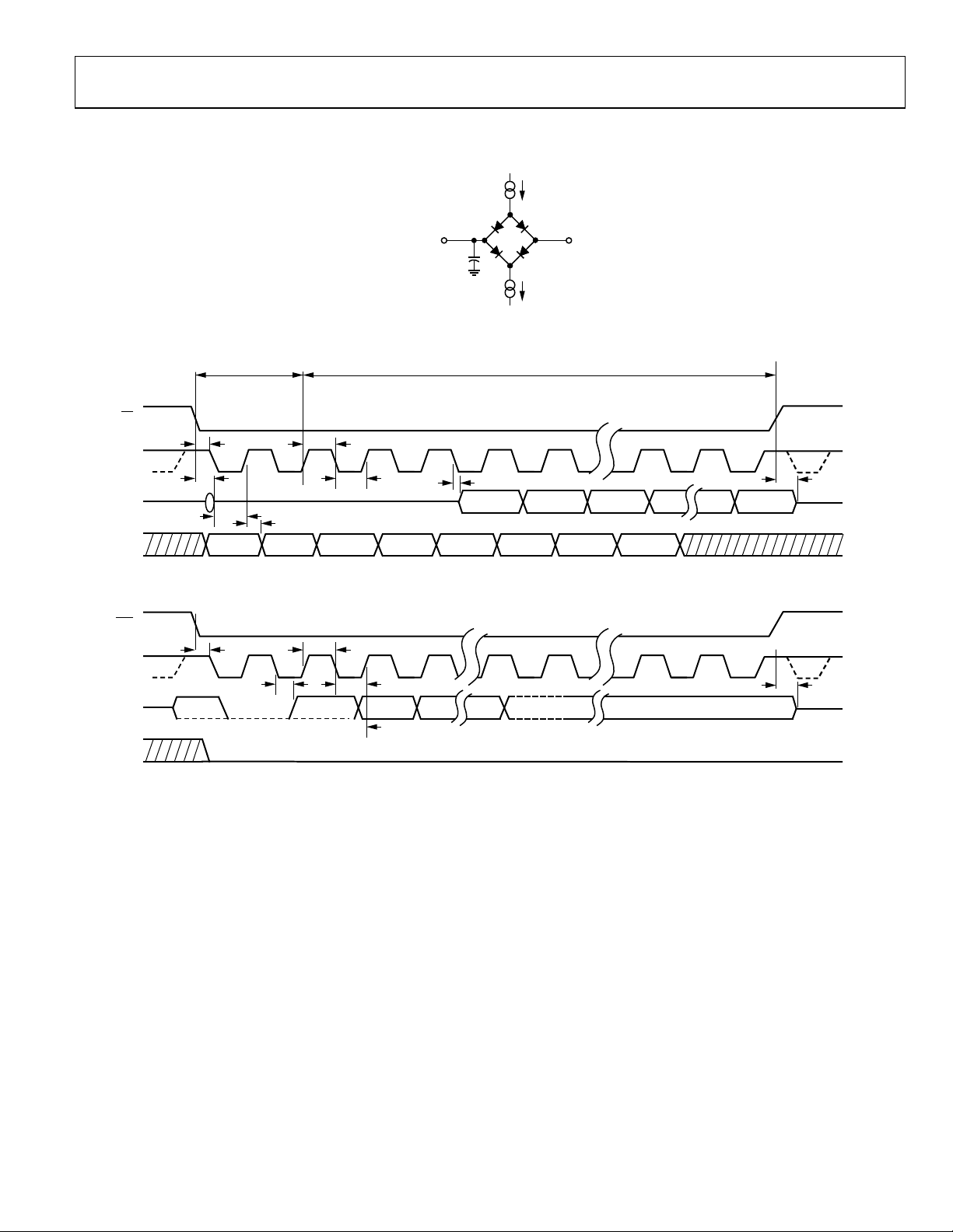
Figure 2. Load Circuit for Digital Output Timing Specifications
t
ACQ
CS
t
1
SCLK
THREE-STATE THREE-STATE
DOUT
DIN
t
2
1
t
4
DONTC
t
5
t
6
234
t
7
4 LEADING ZEROS
ZERO ZERO ZERO ADD0 ONE ZERO PM0
56 15
Figure 3. Accelerometer Serial Interface Timing Diagram
t
3
DB11
t
CONVERT
DB10
16
DB9 DB0
t
8
05463-003
TCS
t
1
SCLK
THREESTATE THREE-STATE
DOUT
1
LEADING
ZERO
t
6
234
t
3
t
7
DB9 DB8
11 15
DB0
16
t
8
DIN
05463-004
Figure 4. Temperature Serial Interface Timing Diagram
Rev. B | Page 5 of 16
 Loading...