

PRELIMINARY TECHNICAL DA T A
a
FEATURES
Low On Resistance < 0.5
ΩΩ
0.1
Ω On Resistance Flatness
ΩΩ
+1.8 V to +5.5 V Single Supply
100pA Leakage Currents
14ns Switching Times
Extended Temperature Range -40
High Current Carrying Capability
Tiny 6 lead SOT23 and 8 Lead
Low Power Consumption
TTL/CMOS Compatible Inputs
Pin Compatible with ADG701/ADG702
APPLICATIONS
Power Routing
Audio and Video Signal Routing
Cellular Phones
Modems
PCMCIA Cards
Hard Drives
Data Acquisition Systems
Communication Systems
Relay replacement
Audio and Video Switching
Battery Powered Systems
ΩΩ
Ω max at 5 V supply
ΩΩ
o
C to +125oC
µµ
µSOIC Packages
µµ
<0.5
ΩΩ
Ω
ΩΩ
CMOS, Low Voltage, SPST Switches
ADG801/ADG802
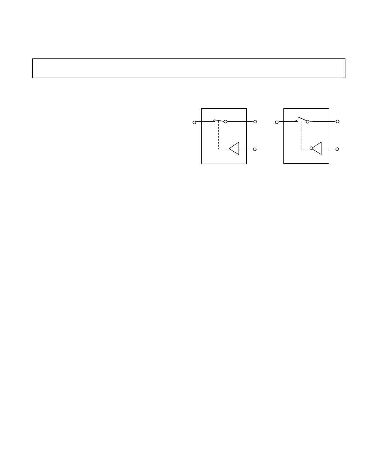
FUNCTIONAL BLOCK DIAGRAMS
ADG801
S
SWITCHES SHOWN FOR A LOGIC "1" INPUT
D
IN
ADG802
S
D
IN
GENERAL DESCRIPTION
The ADG801/ADG802 are monolithic CMOS SPST (Single
Pole, Single Throw) switches with On Resistance of less than
0.5Ω. These switches are designed on an advanced submicron
process that provides extremely low on resistance, high switching speed and low leakage currents.
The low On Resistance of <0.5Ω means these parts are ideal
for applications where low on resistance switching is critical.
The ADG801 is a normally open (NO) switch, while the
ADG802 is normally closed (NC). Each switch conducts
equally well in both directions when ON.
The ADG801 and ADG802 are available in 6-lead SOT-23
and 8 Lead µSOIC packages.
REV. PrE Jan ‘02
Information furnished by Analog Devices is believed to be accurate and
reliable. However, no responsibility is assumed by Analog Devices for its
use, nor for any infringements of patents or other rights of third parties
which may result from its use. No license is granted by implication or
otherwise under any patent or patent rights of Analog Devices.
PRODUCT HIGHLIGHTS
1. Low On Resistance (0.25 Ω typical).
2. +1.8V to +5.5V Single Supply Operation.
3. Tiny 6 Lead SOT23 and 8 Lead µSOIC Packages.
4. Pin Compatible with ADG701 (ADG801)
Pin Compatible with ADG702 (ADG802).
One Technology Way, P.O.Box 9106, Norwood, MA 02062-9106, U.S.A.
Tel: 781/329-4700 www.analog.com
Fax: 781/326-8703 © Analog Devices, Inc., 2002

PRELIMINARY TECHNICAL DA T A
ADG801/ADG802–SPECIFICA TIONS
1
(VDD = 5 V ±10%, VSS = GND = 0 V. All specifications –40°C to +125°C unless otherwise noted.)
–40oC to –40oC to
Parameter +25oC +85oC +125oC Units Test Conditions/Comments
ANALOG SWITCH
Analog Signal Range 0 V to VDDV
On Resistance (R
On-Resistance Flatness (R
LEAKAGE CURRENTS V
Source OFF Leakage I
Drain OFF Leakage ID (OFF) ±0.01 nA typ VS = 4.5 V/1 V, VD = 1 V/4.5 V;
Channel ON Leakage I
DIGITAL INPUTS
Input High Voltage, V
Input Low Voltage, V
Input Current
I
or I
INL
INH
CIN, Digital Input Capacitance 5 pF typ
DYNAMIC CHARACTERISTICS
t
ON
) 0.25 Ω typ VS = 0 V to VDD, IS = –10 mA;
ON
0.4 0.5 0.75 Ω max Test Circuit 1
FLAT(ON)
) 0.05 Ω typ VS = 0 V to VDD, IS = –10 mA
0.1 0.2 Ω max
= +5.5 V
(OFF) ±0.01 nA typ VS = 4.5 V/1 V, VD = 1 V/4.5 V;
S
DD
±0.5 ±1 tbd nA max Test Circuit 2
±0.5 ±1 tbd nA max Test Circuit 2
, IS (ON) ±0.01 nA typ VS = VD = 1 V, or 4.5 V;
D
±0.5 ±1 tbd nA max Test Circuit 3
INH
INL
0.005 µA typ VIN = V
2.4 V min
0.8 V max
INL
or V
INH
±0.1 µA max
2
30 ns typ RL = 50 Ω, CL = 35 pF
TBD TBD ns max V
= 3 V; Test Circuit 4
S
t
OFF
Charge Injection ±20 pC typ V
20 ns typ RL = 50 Ω, CL = 35 pF
TBD TBD ns max V
= 3 V; Test Circuit 4
S
= 0 V, RS = 0 Ω, CL = 1 nF, Test
S
Circuit 5
Off Isolation –65 dB typ R
= 50 Ω, CL = 5 pF, f = 1 MHz,
L
Test Circuit 6
Bandwidth –3 dB 30 MHz typ R
C
(OFF) 55 pF typ f = 1 MHz
S
C
(OFF) 55 pF typ f = 1 MHz
D
= 50 Ω, CL = 5 pF, Test Circuit 7
L
CD, CS (ON) 110 pF typ f = 1 MHz
POWER REQUIREMENTS V
I
DD
0.001 µA typ Digital Inputs = 0 V or 5.5 V
DD
1.0 µA max
NOTES
1
Temperature ranges are as follows: Extended Temperature Range: –40°C to +125°C.
2
Guaranteed by design, not subject to production test.
Specifications subject to change without notice.
= +5.5 V
–2–
REV. PrE

PRELIMINAR Y TECHNICAL DA T A
ADG801/ADG802
1
SPECIFICA TIONS
Parameter +25oC +85oC +125oC Units Test Conditions/Comments
ANALOG SWITCH
Analog Signal Range 0 V to VDDV
On Resistance (R
On-Resistance Flatness(R
LEAKAGE CURRENTS V
Source OFF Leakage I
Drain OFF Leakage I
Channel ON Leakage I
DIGITAL INPUTS
Input High Voltage, V
Input Low Voltage, V
Input Current
I
or I
INL
INH
CIN, Digital Input Capacitance 5 pF typ
DYNAMIC CHARACTERISTICS
t
ON
t
OFF
Charge Injection ±20 pC typ V
Off Isolation –65 dB typ R
Bandwidth –3 dB 30 MHz typ R
C
(OFF) 55 pF typ f = 1 MHz
S
C
(OFF) 55 pF typ f = 1 MHz
D
CD, CS (ON) 110 pF typ f = 1 MHz
POWER REQUIREMENTS V
I
DD
NOTES
1
Temperature ranges are as follows: Extended Temperature Range: –40°C to +125°C.
2
Guaranteed by design, not subject to production test.
Specifications subject to change without notice.
) 0.3 1 Ω typ VS = 0 V to VDD, IS = –10 mA;
ON
D
INH
INL
(VDD = 2.7 V to 3.6 V, VSS = GND = 0 V. All specifications –40°C to +125°C unless otherwise noted.)
–40oC to –40oC to
0.7 0.8 Ω max Test Circuit 1
FLAT(ON)
(OFF) ±0.01 nA typ VS = 3 V/1 V, VD = 1 V/3 V;
S
) 0.1 0.3 Ω typ VS = 0 V to VDD, IS = –10 mA
= +3.3 V
DD
±0.5 ±0.1 tbd nA max Test Circuit 2
(OFF) ±0.01 nA typ VS = 3 V/1 V, VD = 1 V/3 V;
±0.5 ±0.1 tbd nA max Test Circuit 2
, IS (ON) ±0.01 nA typ VS = VD = 1 V, or 3 V;
D
±0.5 ±0.1 tbd nA max Test Circuit 3
2.0 V min
0.4 V max
0.005 µA typ VIN = V
INL
or V
INH
±0.1 µA max
2
50 ns typ RL = 50 Ω, CL = 35 pF
TBD TBD ns max V
= 1.5 V, Test Circuit 4
S
40 ns typ RL = 50 Ω, CL = 35 pF
TBD TBD ns max V
= 0 V, RS = 0 Ω, CL = 1 nF, Test
S
= 1.5 V, Test Circuit 4
S
Circuit 5
= 50 Ω, CL = 5 pF, f = 1 MHz,
L
Test Circuit 6
= 50 Ω, CL = 5 pF, Test Circuit 7
L
= +3.3 V
DD
0.001 µA typ Digital Inputs = 0 V or 3.3 V
1.0 µA max
REV. PrE
–3–
PRELIMINARY TECHNICAL DA T A
WARNING!
ESD SENSITIVE DEVICE
TOP VIEW
(Not to Scale)
8
7
6
5
1
2
3
4
NC = NO CONNECT
D
NC
NC
S
GND
IN
NCV
DD
ADG801/
ADG802
ADG801/ADG802
ABSOLUTE MAXIMUM RATINGS
(TA = +25°C unless otherwise noted)
VDD to GND . . . . . . . . . . . . . . . . . . . . . . . . . . .–0.3 V to +7 V
Analog Inputs
2
. . . . . . . . . . . . . . . . . . . . . . . . . . . . .
. . . . . . . . . . . . . . . . . . . . or 30 mA, Whichever Occurs First
Continuous Current, S or D . . . . . . . . . . . . . . . . . . . . 400 mA
Peak Current, S or D . . . . . . . . . . . . . . . . . . . . . . . . . 800 mA
(Pulsed at 1 ms, 10% Duty Cycle Max)
Operating Temperature Range
Extended . . . . . . . . . . . . . . . . . . . . . . . –40°C to +125°C
Storage Temperature Range . . . . . . . . . –65°C to +150°C
Junction Temperature . . . . . . . . . . . . . . . . . . . . . . . .+150°C
µSOIC Package, Power Dissipation . . . . . . . . . . . 315 mW
θ
Thermal Impedance . . . . . . . . . . . . . . . . . . 206°C/W
JA
θ
Thermal Impedance . . . . . . . . . . . . . . . . . . . 44°C/W
JC
SOT-23 Package, Power Dissipation . . . . . . . . . . 282 mW
θ
Thermal Impedance . . . . . . . . . . . . . . . . .229.6°C/W
JA
θ
Thermal Impedance . . . . . . . . . . . . . . . . .91.99°C/W
JC
Lead Temperature, Soldering (10seconds) . . . . . . . 300°C
IR Reflow, Peak Temperature . . . . . . . . . . . . . . . . .+220°C
ESD.....................................................................2kV
1
- 0.3 V to VDD +0.3 V
NOTES
1
Stresses above those listed under Absolute Maximum Ratings may
cause permanent damage to the device. This is a stress rating only;
functional operation of the device at these or any other conditions above
those listed in the operational sections of this specification is not implied.
Exposure to absolute maximum rating conditions for extended periods
may affect device reliability. Only one absolute maximum rating may
be applied at any one time.
2
Overvoltages at IN, S or D will be clamped by internal diodes. Current should be
limited to the maximum ratings given.
Table I. Truth Table
ADG801 In ADG802 In Switch Condition
0 1 OFF
10ON
PIN CONFIGURATIONS
6-Lead Plastic Surface Mount (SOT-23)
(RT-6)
1
D
ADG801/
2
S
ADG802
TOP VIEW
GND
3
(Not to Scale)
NC = NO CONNECT
6
V
DD
NC
5
IN
4
8-Lead Small Outline
(RM-8)
µµ
µSOIC
µµ
ORDERING GUIDE
Model Temperature Range Supply Option1Brand1Package Descriptions Package Options
ADG801BRT –40°C to +125°C 3 V, 5 V S LB SOT-23 (Plastic Surface Mount) RT-6
ADG801BRM –40°C to +125°C 3 V, 5 V SL B µSOIC (Small Outline) RM-8
ADG802BRT –40°C to +125°C 3 V, 5 V S MB SOT-23 (Plastic Surface Mount) RT-6
ADG802BRM –40°C to +125°C 3 V, 5 V SM B µSOIC (Small Outline) RM-8
1
Branding on SOT-23 and µSOIC packages is limited to 3 characters due to space constraints.
CAUTION
ESD (electrostatic discharge) sensitive device. Electrostatic charges as high as 4000 V readily
accumulate on the human body and test equipment and can discharge without detection. Although
the ADG801/ADG802 features proprietary ESD protection circuitry, permanent damage may
occur on devices subjected to high energy electrostatic discharges. Therefore, proper ESD
precautions are recommended to avoid performance degradation or loss of functionality.
–4–
REV. PrE

PRELIMINARY TECHNICAL DA T A
ADG801/ADG802
TERMINOLOGY
V
DD
I
DD
GND Ground (0 V) reference.
S Source terminal. May be an input or output.
D Drain terminal. May be an input or output.
IN Logic control input.
V
) Analog voltage on terminals D, S
D (VS
R
ON
R
FLAT(ON)
I
(OFF) Source leakage current with the switch “OFF.”
S
(OFF) Drain leakage current with the switch “OFF.”
I
D
I
, IS (ON) Channel leakage current with the switch “ON.”
D
V
INL
V
INH
I
INL(IINH
C
(OFF) “OFF” switch source capacitance. Measured with reference to ground.
S
(OFF) “OFF” switch drain capacitance. Measured with reference to ground.
C
D
C
(ON) “ON” switch capacitance. Measured with reference to ground.
D,CS
C
IN
t
ON
t
OFF
Charge A measure of the glitch impulse transferred from the digital input to the analog output during switching.
Injection
Off Isolation A measure of unwanted signal coupling through an “OFF” switch.
Crosstalk A measure of unwanted signal which is coupled through from one channel to another as a result of parasitic
Bandwidth The frequency at which the output is attenuated by 3dBs.
On Response The Frequency response of the “ON” switch.
Insertion The loss due to the ON resistance of the switch.
Loss
Most positive power supply potential.
Positive supply current.
Ohmic resistance between D and S.
Flatness is defined as the difference between the maximum and minimum value of on-resistance as measured
over the specified analog signal range.
Maximum input voltage for logic “0”.
Minimum input voltage for logic “1”.
) Input current of the digital input.
Digital input capacitance.
Delay between applying the digital control input and the output switching on. See Test Circuit 4.
Delay between applying the digital control input and the output switching off.
capacitance.
REV. PrE
–5–

PRELIMINARY TECHNICAL DA T A
ADG801/ADG802
TYPICAL PERFORMANCE CHARACTERISTICS
TBD
Figure 1. On Resistance as a Function
D(VS
)
of V
TBD
Figure 2. On Resistance as a Function
of VD(VS) for Different Temperatures
TBD
Figure 4. Leakage Currents as a func-
tion of V
D(VS
)
TBD
Figure 5. Leakage Currents as a func-
tion of VD(VS)
TBD
Figure 7. Leakage Currents as a
Function of Temperature
TBD
Figure 8. Supply Currents vs. Input
Switching Frequency
TBD
Figure 3. On Resistance as a Function
of V
) for Different Temperatures
D(VS
TBD
Figure 6. Leakage Currents as a func-
tion of Temperature
–6–
TBD
Figure 9. Charge Injection vs. Source
Voltage
REV. PrE

PRELIMINARY TECHNICAL DA T A
ADG801/ADG802
TBD
Figure 10. TON/T
Times vs. Tem-
OFF
perature
TBD
Figure 11. Off Isolation vs. Frequency
TBD
Figure 13. On Response vs. Fre-
quency
TBD
Figure 12. Crosstalk vs. Frequency
REV. PrE
–7–

ADG801/ADG802
I
DS
V1
SD
V
S
RON = V1/I
DS
SD
A
V
D
I
D (ON)
NC
NC=No Connect
Test Circuits
PRELIMINARY TECHNICAL DA T A
IS (OFF) ID (OFF)
SD
A A
Test Circuit 1. On Resistance
0.1µF
V
S
V
S
IN
R
S
V
S
V
DD
V
DD
SD
GND
Test Circuit 4. Switching Times
V
DD
V
DD
SD
IN
GND
V
D
Test Circuit 2. Off Leakage
ADG801
V
IN
V
R
L
300⍀
C
1nF
OUT
C
L
35pF
V
OUT
L
V
IN
ADG802
V
OUT
V
ADG801
IN
V
ADG802
IN
V
OUT
50% 50%
50% 50%
90% 90%
t
ON
ON
Q
= CL ⴛ ⌬V
INJ
OUT
Test Circuit 3. On Leakage
t
OFF
OFF
⌬V
OUT
0.1µF
IN
V
IN
V
DD
V
DD
S
D
GND
50
Ω
OFF ISOLATION = 20 LOG
Test Circuit 6. Off Isolation
Test Circuit 5. Charge Injection
NETWORK
ANALYZER
50
Ω
V
S
V
OUT
R
L
50
Ω
V
OUT
V
S
–8–
V
0.1µF
IN
V
IN
DD
V
DD
S
D
GND
INSERTION LOSS = 20 LOG
NETWORK
ANALYZER
50
Ω
V
OUT
R
L
50
Ω
V
WITH SWITCH
OUT
V
WITHOUT SWITCH
OUT
V
S
Test Circuit 7. Bandwidth
REV. PrE
PRELIMINARY TECHNICAL DA T A
0.122 (3.10)
0.106 (2.70)
PIN 1
0.118 (3.00)
0.098 (2.50)
0.075 (1.90)
BSC
0.037 (0.95) BSC
1
3
4 5 6
2
0.071 (1.80)
0.059 (1.50)
0.009 (0.23)
0.003 (0.08)
0.022 (0.55)
0.014 (0.35)
10ⴗ
0ⴗ
0.020 (0.50)
0.010 (0.25)
0.006 (0.15)
0.000 (0.00)
0.051 (1.30)
0.035 (0.90)
SEATING
PLANE
0.057 (1.45)
0.035 (0.90)
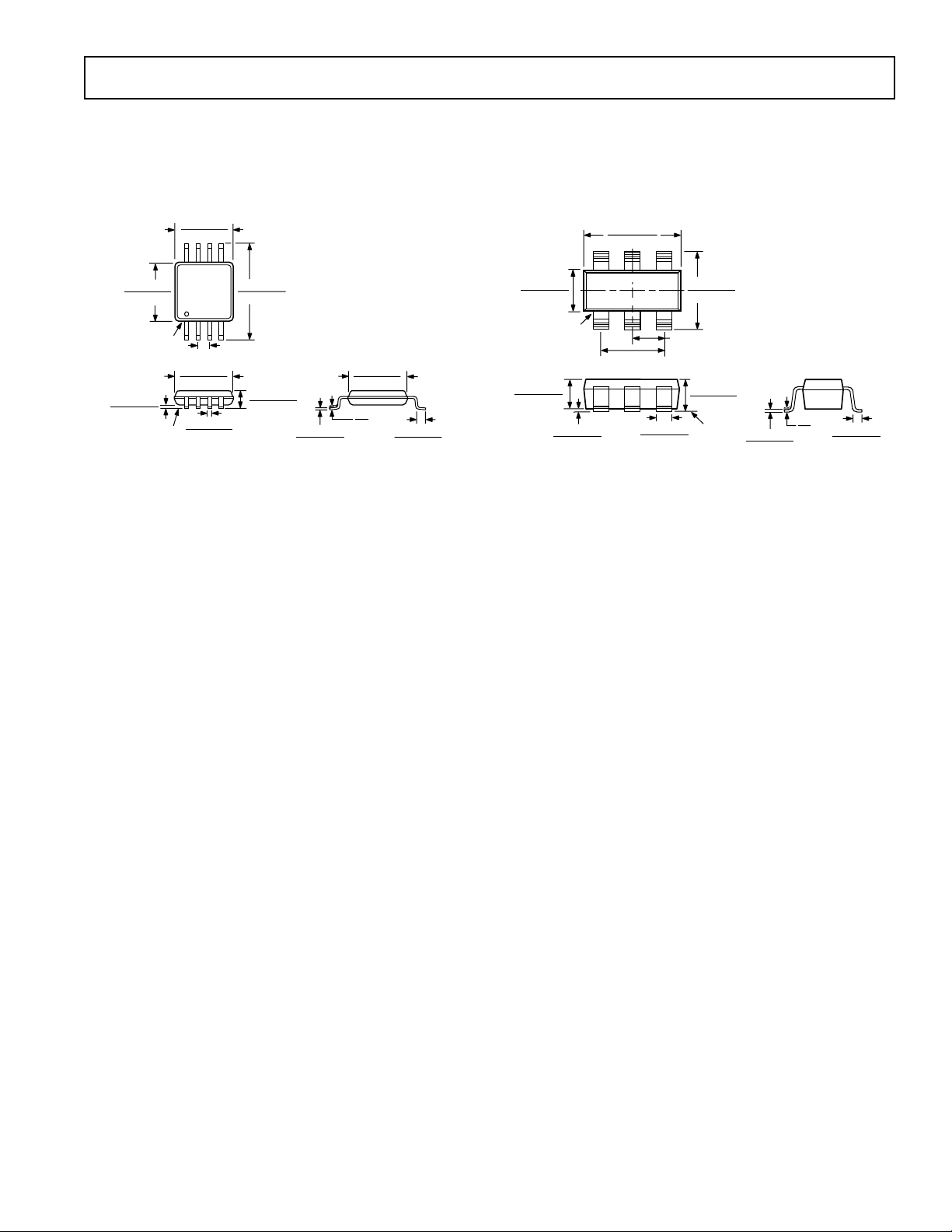
OUTLINE DIMENSIONS
Dimensions shown in inches and (mm).
ADG801/ADG802
0.122 (3.10)
0.114 (2.90)
0.006 (0.15)
0.002 (0.05)
SEATING
PLANE
0.122 (3.10)
0.114 (2.90)
85
1
PIN 1
0.0256 (0.65) BSC
0.120 (3.05)
0.112 (2.84)
0.018 (0.46)
0.008 (0.20)
8-Lead
0.199 (5.05)
0.187 (4.75)
4
µµ
µSOIC
µµ
(RM-8)
0.043 (1.09)
0.037 (0.94)
0.011 (0.28)
0.003 (0.08)
0.120 (3.05)
0.112 (2.84)
33°
27°
6-Lead SOT-23
(RT-6)
0.028 (0.71)
0.016 (0.41)
REV. PrE
–9–
 Loading...