<0.4 Ω CMOS 1.8 V to 5.5 V
www.BDTIC.com/ADI
FEATURES
0.4 Ω maximum on resistance @ 125°C
0.08 Ω maximum on resistance flatness @ 125°C
1.8 V to 5.5 V single supply
Automotive temperature range from −40°C to +125°C
400 mA current-carrying capability
Tiny 6-lead SOT-23, 8-lead MSOP, and 6-ball WLCSP packages
35 ns switching times
Low power consumption
TTL-/CMOS-compatible inputs
Pin compatible with ADG701/ADG702
APPLICATIONS
Power routing
Cellular phones
Modems
PCMCIA cards
Hard drives
Data acquisition systems
Communications systems
Relay replacement
Battery-powered systems
SPST Switches
ADG801/ADG802
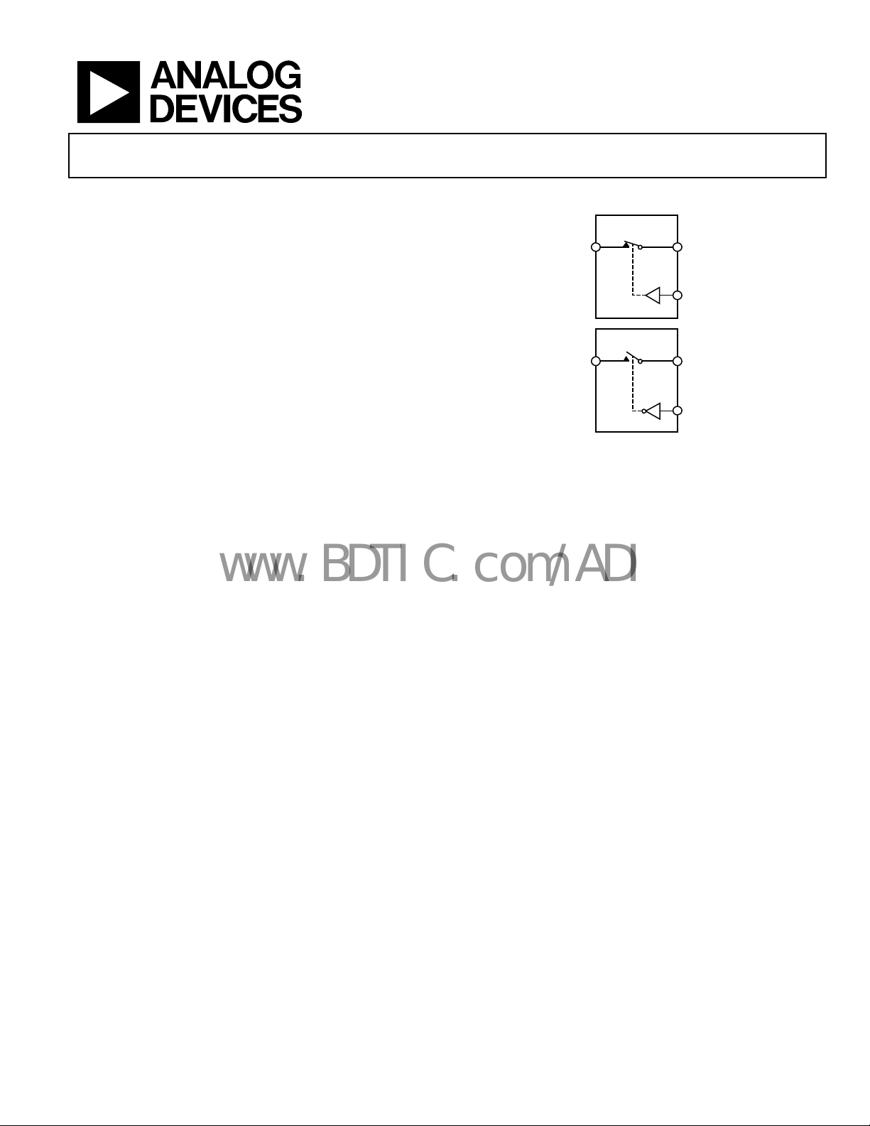
FUNCTIONAL BLOCK DIAGRAM
ADG801
S
ADG802
S
SWITCHES SHOWN FOR
A LOGIC 1 INPUT
Figure 1.
D
IN
D
IN
02800-001
GENERAL DESCRIPTION
The ADG801 and ADG802 are monolithic CMOS, single-pole,
single throw (SPST) switches with on resistance of less than
0.4 Ω. These switches are designed using an advanced
submicron process that provides extremely low on resistance,
high switching speed, and low leakage currents.
The low on resistance of <0.4 Ω makes these parts ideal for
a
pplications where low on resistance switching is critical.
The ADG801 switch is normally open (NO), while the ADG802
is n
ormally closed (NC). Each switch conducts equally well in
both directions when on.
PRODUCT HIGHLIGHTS
1. Low on resistance (0.25 Ω typical).
2. 1.8 V t
3. T
4. 400 mA c
5. A
6. P
o 5.5 V single-supply operation.
iny 6-lead SOT-23, 8-lead MSOP, and 6-ball WLCSP
packages.
urrent-carrying capability.
utomotive temperature range from −40°C to +125°C.
in compatible with ADG701 (ADG801) and ADG702
(ADG802).
Rev. A
Information furnished by Analog Devices is believed to be accurate and reliable. However, no
responsibility is assumed by Anal og Devices for its use, nor for any infringements of patents or ot her
rights of third parties that may result from its use. Specifications subject to change without notice. No
license is granted by implication or otherwise under any patent or patent rights of Analog Devices.
Trademarks and registered trademarks are the property of their respective owners.
One Technology Way, P.O. Box 9106, Norwood, MA 02062-9106, U.S.A.
Tel: 781.329.4700 www.analog.com
Fax: 781.461.3113 ©2002–2007 Analog Devices, Inc. All rights reserved.

ADG801/ADG802
www.BDTIC.com/ADI
TABLE OF CONTENTS
Features.............................................................................................. 1
Applications....................................................................................... 1
Functional Block Diagram .............................................................. 1
General Description ......................................................................... 1
Product Highlights ........................................................................... 1
Revision History ............................................................................... 2
Specifications..................................................................................... 3
Absolute Maximum Ratings............................................................ 5
REVISION HISTORY
3/07—Rev. 0 to Rev. A
Updated Format..................................................................Universal
Added 6-Ball WLCSP Package (Text and Figures) ........Universal
Replaced Typical Performance Characteristics Section .............. 8
Updated Outline Dimensions....................................................... 12
Changes to Ordering Guide.......................................................... 14
5/02—Revision 0: Initial Version
ESD Caution...................................................................................5
Pin Configuration and Function Descriptions..............................6
Terminology.......................................................................................7
Typical Performance Characteristics..............................................8
Test Circuits..................................................................................... 10
Outline Dimensions....................................................................... 12
Ordering Guide .......................................................................... 14
Rev. A | Page 2 of 16

ADG801/ADG802
www.BDTIC.com/ADI
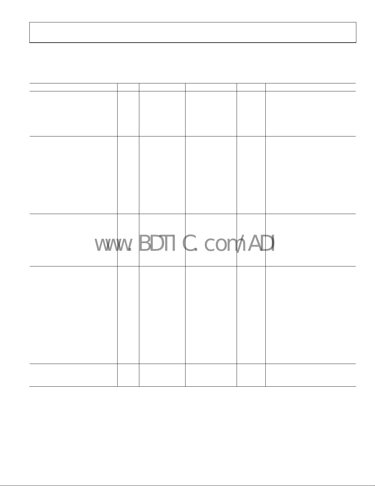
SPECIFICATIONS
VDD = 5 V ± 10%, GND = 0 V, unless otherwise noted. The automotive temperature range is −40°C to +125°C.
Table 1.
Parameter 25°C −40°C to +85°C −40°C to +125°C1Unit Test Conditions/Comments
ANALOG SWITCH
Analog Signal Range 0 V to VDD V
On Resistance (RON) 0.25 Ω typ VS = 0 V to VDD, IS = 100 mA; Test Circuit 1
0.3 0.35 0.4 Ω max VS = 0 V to VDD, IS = 100 mA; Test Circuit 1
On Resistance Flatness (R
0.07 0.08 Ω max
LEAKAGE CURRENTS VDD = 5.5 V
Source Off Leakage, IS (Off) ±0.01 nA typ
±0.25 ±3 ±30 nA max
Drain Off Leakage, ID (Off) ±0.01 nA typ
±0.25 ±3 ±30 nA max
Channel On Leakage, ID, IS (On) ±0.01 nA typ VS = VD = 1 V, or 4.5 V; Test Circuit 3
±0.25 ±3 ±30 nA max VS = VD = 1 V, or 4.5 V; Test Circuit 3
DIGITAL INPUTS
Input High Voltage, V
Input Low Voltage, V
INH
0.8 V max
INL
Input Current
I
or I
0.005 μA typ VIN = V
INL
INH
±0.1 μA max
CIN, Digital Input Capacitance 5 pF typ
DYNAMIC CHARACTERISTICS2
tON 35 ns typ RL = 50 Ω, CL = 35 pF
45 50 55 ns max VS = 3 V; Test Circuit 4
t
9 ns typ RL = 50 Ω, CL = 35 pF
OFF
15 18 21 ns max VS = 3 V; Test Circuit 4
Charge Injection 50 pC typ VS = 2.5 V, RS = 0 Ω; CL = 1 nF;
Test Circuit 5
Off Isolation −61 dB typ RL = 50 Ω, CL = 5 pF; f = 100 kHz;
Test Circuit 6
Bandwidth −3 dB 12 MHz typ RL = 50 Ω, CL = 5 pF; Test Circuit 7
CS (Off) 180 pF typ f = 1 MHz
CD (Off) 180 pF typ f = 1 MHz
CD, CS (On) 420 pF typ f = 1 MHz
POWER REQUIREMENTS VDD = 5.5 V
IDD 0.001 μA typ Digital inputs = 0 V or 5.5 V
1.0 2.0 μA max
1
On resistance parameters tested with IS = 10 mA.
2
Guaranteed by design, not subject to production test.
) 0.05 Ω typ VS = 0 V to VDD, IS = 100 mA
FLAT(ON)
= 4.5 V/1 V, VD = 1 V/4.5 V; Test
V
S
Circuit 2
= 4.5 V/1 V, VD = 1 V/4.5 V; Test
V
S
Circuit 2
= 4.5 V/1 V, VD = 1 V/4.5 V; Test
V
S
Circuit 2
= 4.5 V/1 V, VD = 1 V/4.5 V; Test
V
S
Circuit 2
2.0 V min
or V
INL
INH
Rev. A | Page 3 of 16

ADG801/ADG802
www.BDTIC.com/ADI
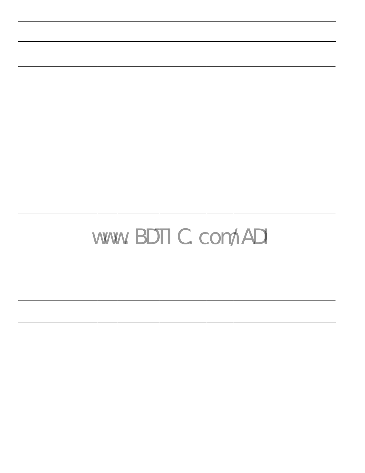
VDD = 2.7 V to 3.6 V, GND = 0 V, unless otherwise noted. The automotive temperature range is −40°C to +125°C.
Table 2.
Parameter 25°C −40°C to +85°C −40°C to +125°C1 Unit Test Conditions/Comments
ANALOG SWITCH
Analog Signal Range 0 V to VDD V
On Resistance (RON) 0.4 Ω typ VS = 0 V to VDD, IS = 100 mA; Test Circuit 1
0.6 0.65 0.7 Ω max VS = 0 V to VDD, IS = 100 mA; Test Circuit 1
On Resistance Flatness (R
LEAKAGE CURRENTS VDD = 3.6 V
Source Off Leakage, IS (Off) ±0.01 nA typ VS = 3.3 V/1 V, VD = 1 V/3.3 V; Test Circuit 2
±0.25 ±3 ±30 nA max VS = 3.3 V/1 V, VD = 1 V/3.3 V; Test Circuit 2
Drain Off Leakage, ID (Off) ±0.01 nA typ VS = 3.3 V/1 V, VD = 1 V/3.3 V; Test Circuit 2
±0.25 ±3 ±30 nA max VS = 3.3 V/1 V, VD = 1 V/3.3 V; Test Circuit 2
Channel On Leakage, ID, IS (On) ±0.01 nA typ VS = VD = 1 V, or 3.3 V; Test Circuit 3
±0.25 ±3 ±30 nA max VS = VD = 1 V, or 3.3 V; Test Circuit 3
DIGITAL INPUTS
Input High Voltage, V
Input Low Voltage, V
INL
Input Current
I
or I
0.005 μA typ VIN = V
INL
INH
±0.1 μA max
CIN, Digital Input Capacitance 5 pF typ
DYNAMIC CHARACTERISTICS2
tON 40 ns typ RL = 50 Ω, CL = 35 pF
55 60 65 ns max VS = 1.5 V; Test Circuit 4
t
9 ns typ RL = 50 Ω, CL = 35 pF
OFF
15 18 21 ns max VS = 1.5 V; Test Circuit 4
Charge Injection 10 pC typ VS = 1.5 V, RS = 0 Ω, CL = 1 nF; Test Circuit 5
Off Isolation −61 dB typ RL = 50 Ω, CL = 5 pF, f = 100 kHz;
Test Circuit 6
Bandwidth −3 dB 12 MHz typ RL = 50 Ω, CL = 5 pF; Test Circuit 7
CS (Off) 180 pF typ f = 1 MHz
CD (Off) 180 pF typ f = 1 MHz
CD, CS (On) 420 pF typ f = 1 MHz
POWER REQUIREMENTS VDD = 3.6 V
IDD 0.001 μA typ Digital inputs = 0 V or 3.6 V
1.0 2.0 μA max
1
On resistance parameters tested with IS = 10 mA.
2
Guaranteed by design, not subject to production test.
) 0.1 0.1 0.1 Ω typ VS = 0 V to VDD, IS = 100 mA
FLAT(ON)
2.0 V min
INH
0.8 V max
or V
INL
INH
Rev. A | Page 4 of 16

ADG801/ADG802
www.BDTIC.com/ADI
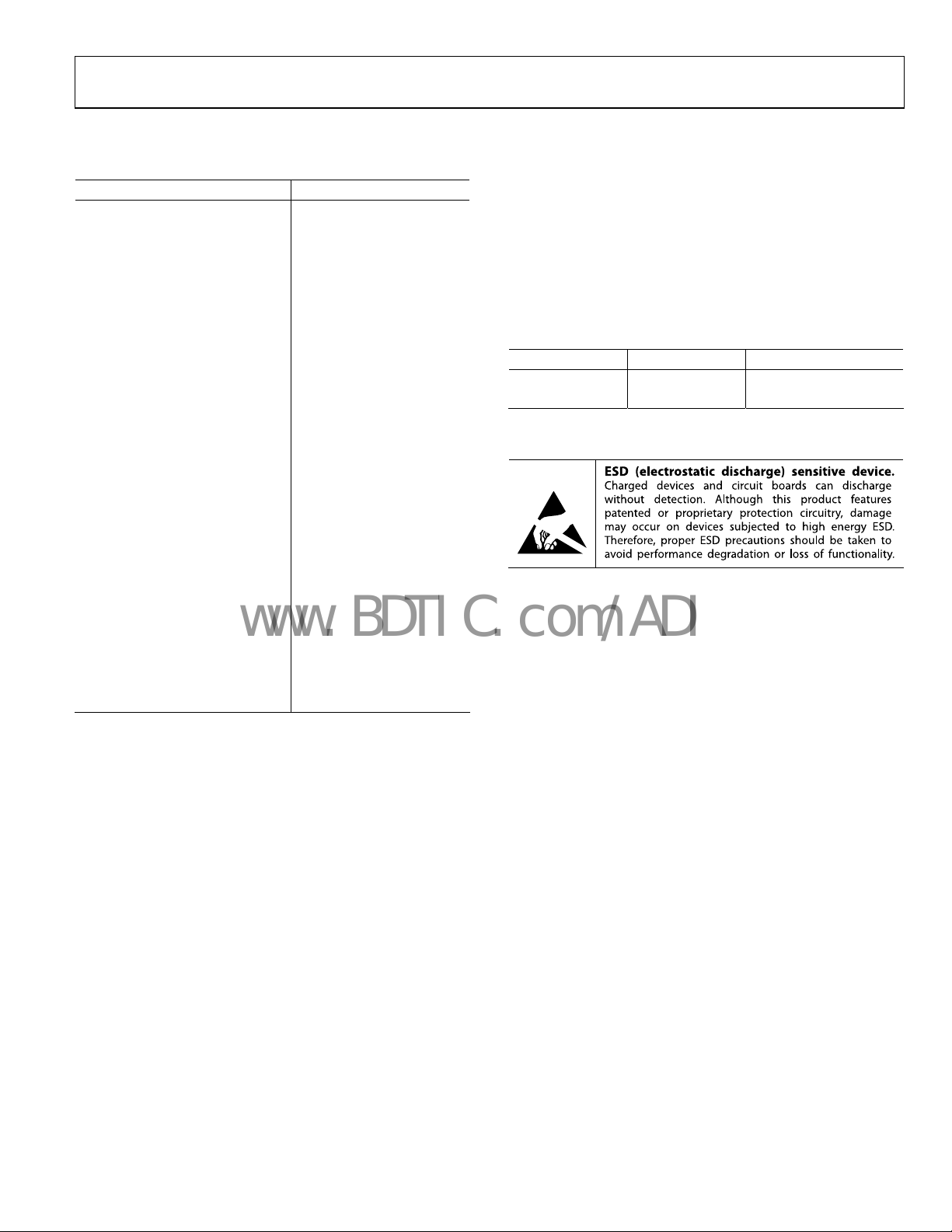
ABSOLUTE MAXIMUM RATINGS
TA = 25°C, unless otherwise noted.
Parameter Rating
VDD to GND −0.3 V to +7 V
Analog Inputs1
Digital Inputs1
Continuous Current, Pin S or Pin D 400 mA
Peak Current, Pin S or Pin D
Operating Temperature Range
tomotive
Au
Storage Temperature Range −65°C to +150°C
Junction Temperature (T
Package Power Dissipation ( T
MSOP
θJA Thermal Impedance 206°C/W
θJC Thermal Impedance 44°C/W
SOT-23 (4-Layer Board)
θJA Thermal Impedance 119°C/W
θJC Thermal Impedance 91.99°C/W
WLCSP (4-Layer Board)
θJA Thermal Impedance 120°C/W
Lead Temperature, Soldering
(10 sec)
IR Reflow, Peak Temperature
(<20 sec)
Reflow Soldering (Pb-Free)
Peak Temperature 260(+0/−5)°C
Time at Peak Temperature 10 sec to 40 sec
1
Overvoltages at Pin IN, Pin S, or Pin D are clamped by internal diodes.
Current should be limited to the maximum ratings provided.
) 150°C
JMAX
−0.3 V to VDD + 0.3 V or
mA, whichever occurs first
30
−0.3 V to VDD + 0.3 V or
mA, whichever occurs first
30
800 mA, pulsed at 1 ms,
10% duty c
−40°C to +125°C
JMAX
300°C
235°C
ycle max
– TA)/θJA
Stresses above those listed under Absolute Maximum Ratings
may cause permanent damage to the device. This is a stress
rating only; functional operation of the device at these or any
other conditions above those indicated in the operational
section of this specification is not implied. Exposure to absolute
maximum rating conditions for extended periods may affect
device reliability.
Table 3. Truth Table
ADG801 (Pin IN) ADG802 (Pin IN) Switch Condition
0 1 Off
1 0 On
ESD CAUTION
Rev. A | Page 5 of 16
 Loading...