ANALOG DEVICES ADG791A Service Manual

I2C-Compatible, Wide Bandwidth,
www.BDTIC.com/ADI
FEATURES
Bandwidth: 325 MHz
Low insertion loss and on resistance: 2.6 Ω typical
On resistance flatness: 0.3 Ω typical
Single 3 V/5 V supply operation
3.3 V analog signal range (5 V supply, 75 Ω load)
Low quiescent supply current:
Fast switching times: t
2
C®-compatible interface
I
ON
Compact 24-lead LFCSP
ESD protection
4 kV human body model (HBM)
200 V machine model (MM)
1 kV field-induced charged device model (FICDM)
APPLICATIONS
S-video RGB/YPbPr video switches
HDTVs
Projection TVs
DVD-R/RW
AV receivers
GENERAL DESCRIPTION
1 nA typical
= 186 ns, t
= 177 ns
OFF
S1A
S1B
S2A
S2B
S3A
S3B
S4A
S4B
Quad, 2:1 Multiplexer
ADG791A/ADG791G
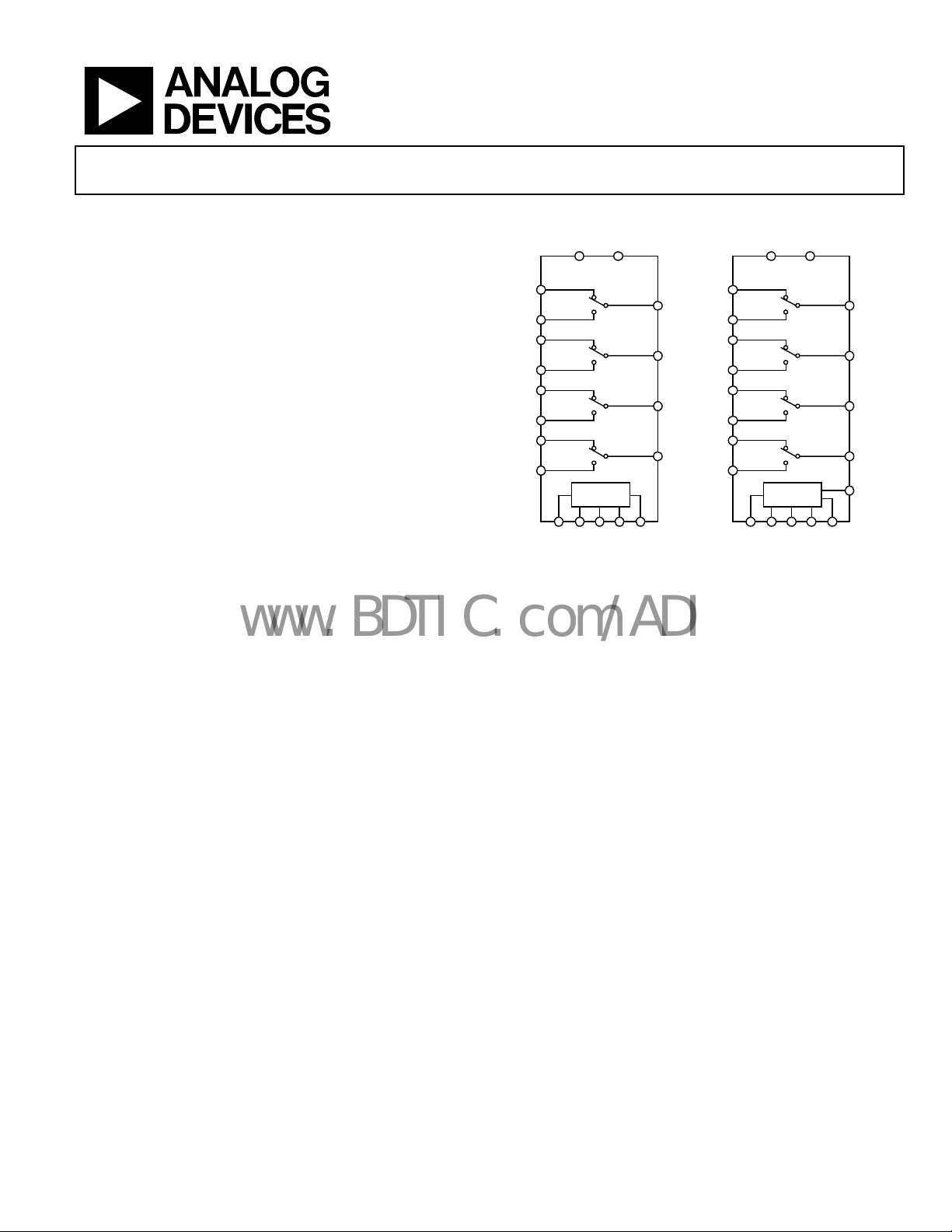
FUNCTIONAL BLOCK DIAGRAM
V
DD
GND
ADG791A
I2C SERIAL
INTERFACE
S1A
D1
S1B
S2A
D2
S2B
S3A
D3
S3B
S4A
D4
S4B
SCLSDAA2A1A0
Figure 1.
V
DD
ADG791G
I2C SERIAL
INTERFACE
GND
D1
D2
D3
D4
GPO1
SCLSDAA2A1A0
06033-001
The ADG791A/ADG791G are monolithic CMOS devices
comprising four 2:1 multiplexers/demultiplexers controllable
via a standard I
2
C serial interface. The CMOS process provides
ultralow power dissipation yet gives high switching speed and
low on resistance.
The on-resistance profile is very flat over the full analog input
r
ange and wide bandwidth ensures excellent linearity and low
distortion. These features, combined with a wide input signal
range make the ADG791A/ADG791G the ideal switching
solution for a wide range of TV applications including S-video,
RGB, and YPbPr video switches.
The switches conduct equally well in both
directions when on.
In the off condition, signal levels up to the supplies are blocked.
The ADG791A/ADG791G switches exhibit break-before-make
switching action. The ADG791G has one general-purpose logic
output pin controlled by the I
to control other non-I
The integrated I
2
2
C interface provides a large degree of flexibility
in the system design. It has three configurable I
2
C interface that can also be used
C-compatible devices such as video filters.
2
C address pins
Rev. 0
Information furnished by Analog Devices is believed to be accurate and reliable. However, no
responsibility is assumed by Anal og Devices for its use, nor for any infringements of patents or ot her
rights of third parties that may result from its use. Specifications subject to change without notice. No
license is granted by implication or otherwise under any patent or patent rights of Analog Devices.
Trademarks and registered trademarks are the property of their respective owners.
that allow up to eight devices on the same bus. This allows the
er to expand the capability of the device by increasing the size
us
of the switching array.
The ADG791A/ADG791G operate from a single 3 V or 5 V
upply voltage and is available in a compact 4 mm × 4 mm
s
body, 24-lead LFCSP.
PRODUCT HIGHLIGHTS
1. Wide bandwidth: 325 MHz.
2. Ultralow power dissipation.
3. Extended input signal range.
4. Integrated I
5. Compact 4 mm × 4 mm, 24-lead, Pb-free LFCSP.
6. ESD protection tested as per ESD association standards:
4 kV HBM (ANS
200 V MM (ANSI/ESD STM5.2-1999)
1 kV FICDM (ANSI/ESDSTM5.3.1-1999)
One Technology Way, P.O. Box 9106, Norwood, MA 02062-9106, U.S.A.
Tel: 781.329.4700 www.analog.com
Fax: 781.461.3113 ©2006 Analog Devices, Inc. All rights reserved.
2
C serial interface.
I/ESD STM5.1-2001)

ADG791A/ADG791G
www.BDTIC.com/ADI
TABLE OF CONTENTS
Features .............................................................................................. 1
Te r mi n ol o g y .................................................................................... 16
Applications....................................................................................... 1
Functional Block Diagram .............................................................. 1
General Description......................................................................... 1
Product Highlights ........................................................................... 1
Revision History ............................................................................... 2
Specifications..................................................................................... 3
2
I
C Timing Specifications............................................................ 7
Timing Diagram ........................................................................... 8
Absolute Maximum Ratings............................................................ 9
ESD Caution.................................................................................. 9
Pin Configurations and Function Descriptions .........................10
Typical Performance Characteristics ........................................... 11
Test Cir c ui t s .....................................................................................14
REVISION HISTORY
Theory of Operation ...................................................................... 17
2
I
C Serial Interface ..................................................................... 17
2
I
C Address.................................................................................. 17
Write Operation.......................................................................... 17
LDSW Bit..................................................................................... 19
Power On/Software Reset.......................................................... 19
Read Operation........................................................................... 19
Evaluation Board ............................................................................ 20
Using the ADG791G Evaluation Board .................................. 20
Outline Dimensions ....................................................................... 23
Ordering Guide .......................................................................... 23
7/06—Revision 0: Initial Version
Rev. 0 | Page 2 of 24

ADG791A/ADG791G
www.BDTIC.com/ADI
SPECIFICATIONS
VDD = 5 V ± 10%, GND = 0 V, TA = −40°C to +85°C, unless otherwise noted.
Table 1.
Parameter Conditions Min Typ1 Max Unit
ANALOG SWITCH
Analog Signal Range
V
On Resistance, R
V
On-Resistance Matching Between
Channels, ∆R
V
On-Resistance Flatness, R
LEAKAGE CURRENTS
Source OFF Leakage (IS
Drain OFF Leakage (ID
Channel ON Leakage (ID
DYNAMIC CHARACTERISTICS3
tON, t
t
OFF
CL = 35 pF, RL = 50 Ω, VS = 2 V, see Figure 28 186 250 ns
ENABLE
, t
CL = 35 pF, RL = 50 Ω, VS = 2 V, see Figure 28 177 240 ns
DISABLE
Break-Before-Make Time Delay, t
I2C to GPO Propagation Delay, tH, tL (ADG791G only) 130 ns
Off Isolation f = 10 MHz, RL = 50 Ω, see Figure 26 −60 dB
Channel-to-Channel Crosstalk f = 10 MHz, RL = 50 Ω, see Figure 27
Same Multiplexer
Different Multiplexer
−3 dB Bandwidth RL = 50 Ω, see Figure 25 325 MHz
THD + N RL = 100 Ω 0.14 %
Charge Injection CL = 1 nF, VS = 0 V, see Figure 30 5 pC
CS
(OFF)
CD
(OFF)
CD
, CS
(ON)
(ON)
Power Supply Rejection Ratio, PSRR f = 20 kHz 70 dB
Differential Gain Error CCIR330 test signal 0.32 %
Differential Phase Error CCIR330 test signal 0.44 Degrees
LOGIC INPUTS3
A0, A1, A2
Input High Voltage, V
Input Low Voltage, V
Input Current, I
Input Capacitance, CIN 3 pF
SCL, SDA
Input High Voltage, V
Input Low Voltage, V
Input Leakage Current, IIN VIN = 0 V to VDD 0.005 ±1 μA
Input Hysteresis 0.05 × VDD V
Input Capacitance, CIN 3 pF
2
ON
ON
VD = 0 V to 1 V, IDS = −10 mA 0.3 0.55 Ω
FLAT (ON)
) VD = 4 V/1 V, VS = 1 V/4 V, see Figure 23 ±0.25 nA
(OFF)
) VD = 4 V/1 V, VS = 1 V/4 V, see Figure 23 ±0.25 nA
(OFF)
, IS
(ON)
) VD = VS = 4 V/1 V, see Figure 24 ±0.25 nA
(ON)
D
VS = VDD, RL = 1 MΩ 0 4 V
= VDD, RL = 75 Ω 0 3.3 V
S
VD = 0 V, IDS = −10 mA, see Figure 22 2.6 3.5 Ω
= 0 V to 1 V, IDS = −10 mA, see Figure 22 4 Ω
D
V
= 0 V, IDS = −10 mA
D
= 1 V, IDS = −10 mA 0.6 Ω
D
0.15
0.5
Ω
CL = 35 pF, RL = 50 Ω, VS1 = VS2 = 2 V, see Figure 29 1 3 ns
−55 dB
−70 dB
10 pF
13 pF
27 pF
2.0 V
INH
0.8 V
INL
or I
VIN = 0 V to VDD 0.005 ±1 μA
INL
INH
0.7 × V
INH
−0.3 +0.3 × V
INL
V
DD
+ 0.3 V
DD
DD
V
Rev. 0 | Page 3 of 24

ADG791A/ADG791G
www.BDTIC.com/ADI
Parameter Conditions Min Typ1 Max Unit
LOGIC OUTPUTS
SDA Pin
Output Low Voltage, V
I
Floating-State Leakage Current ±1 μA
Floating-State Output Capacitance 10 pF
GPO1 Pin and GPO2 Pin
Output Low Voltage, V
Output High Voltage, V
POWER REQUIREMENTS
IDD Digital inputs = 0 V or VDD, I2C interface inactive 0.001 1 μA
I
I
1
All typical values are at TA = 25°C, unless otherwise stated.
2
Guaranteed by initial characterization, not subject to production test.
3
Guaranteed by design, not subject to production test.
3
OL
OL
OH
I
= 3 mA 0.4 V
SINK
= 6 mA 0.6 V
SINK
I
= +2 mA 0.4 V
LOAD
I
= −2 mA 2.0 V
LOAD
2
C interface active, f
2
C interface active, f
= 400 kHz 0.2 mA
SCL
= 3.4 MHz 0.7 mA
SCL
Rev. 0 | Page 4 of 24

ADG791A/ADG791G
www.BDTIC.com/ADI
VDD = 3 V ± 10%, GND = 0 V, TA = −40°C to +85°C, unless otherwise noted.
Table 2.
Parameter Conditions Min Typ1 Max Unit
ANALOG SWITCH
Analog Signal Range
V
On Resistance, R
V
On-Resistance Matching Between
Channels, ∆R
ON
V
On-Resistance Flatness, R
LEAKAGE CURRENTS
Source Off Leakage (IS
Drain Off Leakage (ID
Channel On Leakage (ID
DYNAMIC CHARACTERISTICS3
tON, t
t
OFF
CL = 35 pF, RL = 50 Ω, VS = 2 V, see Figure 28 198 270 ns
ENABLE
, t
CL = 35 pF, RL = 50 Ω, VS = 2 V, see Figure 28 195 260 ns
DISABLE
Break-Before-Make Time Delay, t
I2C to GPO Propagation Delay, tH, tL
(ADG791G only)
Off Isolation f = 10 MHz, RL = 50 Ω, see Figure 26 −60 dB
Channel-to-Channel Crosstalk f = 10 MHz, RL = 50 Ω, see Figure 27
Same Multiplexer
Different Multiplexer
−3 dB Bandwidth RL = 50 Ω, see Figure 25 310 MHz
THD + N RL = 100 Ω 0.14 %
Charge Injection CL = 1 nF, VS = 0 V, see Figure 30 2.5 pC
CS
(OFF)
CD
(OFF)
CD
, CS
(ON)
(ON)
Power Supply Rejection Ratio, PSRR f = 20 kHz 70 dB
Differential Gain Error CCIR330 test signal 0.28 %
Differential Phase Error CCIR330 test signal 0.28 Degrees
LOGIC INPUTS
3
A0, A1, A2
Input High Voltage, V
Input Low Voltage, V
Input Current, I
Input Capacitance, CIN 3 pF
SCL, SDA
Input High Voltage, V
Input Low Voltage, V
Input Leakage Current, IIN VIN = 0 V to VDD 0.005 ±1 μA
Input Hysteresis 0.05 × VDD V
Input Capacitance, CIN 3 pF
2
ON
VD = 0 V to 1 V, IDS = −10 mA 0.8 2.8 Ω
FLAT (ON)
) VD = 2 V/1 V, VS = 1 V/2 V, see Figure 23 ±0.25 nA
(OFF)
) VD = 2 V/1 V, VS = 1 V/2 V, see Figure 23 ±0.25 nA
(OFF)
, IS
(ON)
) VD = VS = 2 V/1 V, see Figure 24 ±0.25 nA
(ON)
D
VS = VDD, RL = 1 MΩ 0 2.2 V
= VDD, RL = 75 Ω 0 1.7 V
S
VD = 0 V, IDS = −10 mA, see Figure 22 3 4 Ω
= 0 V to 1 V, IDS = −10 mA, see Figure 22 6 Ω
D
V
= 0 V, IDS = −10 mA
D
= 1 V, IDS = −10 mA 1.1 Ω
D
0.15
CL = 35 pF, RL = 50 Ω, VS1 = VS2 = 2 V, see Figure 29 1 3 ns
121 ns
−55 dB
−70 dB
10 pF
13 pF
27 pF
2.0 V
INH
0.8 V
INL
or I
VIN = 0 V to VDD 0.005 ±1 μA
INL
INH
0.7 × VDD V
INH
−0.3 +0.3 × V
INL
0.6
+ 0.3 V
DD
Ω
V
DD
Rev. 0 | Page 5 of 24

ADG791A/ADG791G
www.BDTIC.com/ADI
Parameter Conditions Min Typ1 Max Unit
LOGIC OUTPUTS
SDA Pin
Output Low Voltage, V
Floating-State Leakage Current ±1 μA
Floating-State Output Capacitance 3 pF
GPO1 Pin and GPO2 Pin
Output Low Voltage, V
Output High Voltage, V
POWER REQUIREMENTS
IDD Digital inputs = 0 V or VDD, I2C interface inactive 0.001 1 μA
I
I
1
All typical values are at TA = 25°C, unless otherwise stated.
2
Guaranteed by initial characterization, not subject to production test.
3
Guaranteed by design, not subject to production test.
3
OL
OL
OH
I
= 3 mA 0.4 V
SINK
I
= 6 mA 0.6 V
SINK
I
= +2 mA 0.4 V
LOAD
I
= −2 mA 2.0 V
LOAD
2
C interface active, f
2
C interface active, f
= 400 kHz 0.1 mA
SCL
= 3.4 MHz 0.2 mA
SCL
Rev. 0 | Page 6 of 24

ADG791A/ADG791G
www.BDTIC.com/ADI
I2C TIMING SPECIFICATIONS
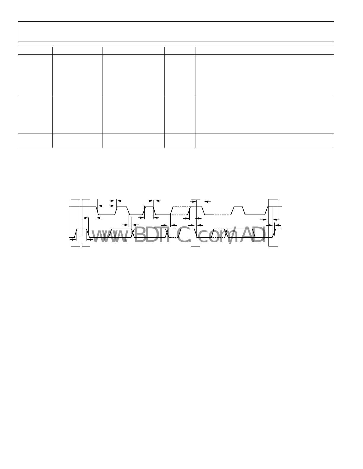
VDD = 2.7 V to 5.5 V; GND = 0 V; TA = −40°C to +85°C, unless otherwise noted. See Figure 2 for timing diagram.
Table 3.
Parameter1Conditions Min Max Unit Description
f
Standard mode 100 kHz Serial clock frequency
SCL
Fast mode 400 kHz
High speed mode
C
C
t1 Standard mode 4 μs t
Fast mode 0.6 μs
High speed mode
C
C
t2 Standard mode 4.7 μs t
Fast mode 1.3 μs
High speed mode
C
C
t
3
Fast mode 100 ns
High speed mode 10 ns
2
t
4
Fast mode 0 0.9 μs
High speed mode
C
C
t5 Standard mode 4.7 μs t
Fast mode 0.6 μs
High speed mode 160 ns
t6 Standard mode 4 μs t
Fast mode 0.6 μs
High speed mode 160 ns
t7 Standard mode 4.7 μs t
Fast mode 1.3 μs
t8 Standard mode 4 μs t
Fast mode 0.6 μs
High speed mode 160 ns
t9 Standard mode 1000 ns t
Fast mode 20 + 0.1 C
High speed mode
C
C
t10 Standard mode 300 ns t
Fast mode 20 + 0.1 C
High speed mode
C
C
t11 Standard mode 1000 ns t
Fast mode 20 + 0.1 C
High speed mode
C
C
= 100 pF max 3.4 MHz
B
= 400 pF max 1.7 MHz
B
= 100 pF max 60 ns
B
= 400 pF max 120 ns
B
= 100 pF max 160 ns
B
= 400 pF max 320 ns
B
Standard mode 250 ns t
Standard mode 0 3.45 μs t
= 100 pF max 0 703 ns
B
= 400 pF max 0 150 ns
B
B 300 ns
B
= 100 pF max 10 80 ns
B
= 400 pF max 20 160 ns
B
B 300 ns
B
= 100 pF max 10 80 ns
B
= 400 pF max 20 160 ns
B
B 300 ns
B
= 100 pF max 10 40 ns
B
= 400 pF max 20 80 ns
B
Rev. 0 | Page 7 of 24
, SCL high time
HIGH
, SCL low time
LOW
, data setup time
SU;DAT
, data hold time
HD;DAT
, setup time for a repeated start condition
SU;STA
, hold time (repeated) start condition
HD;STA
, bus free time between a stop and a start condition
BUF
, setup time for stop condition
SU;STO
, rise time of SDA signal
RDA
, fall time of SDA signal
FDA
, rise time of SCL signal
RCL

ADG791A/ADG791G
S
www.BDTIC.com/ADI
Parameter1Conditions Min Max Unit Description
t
11A
Fast mode 20 + 0.1 C
High speed mode
C
C
t12 Standard mode 300 ns t
Fast mode 20 + 0.1 C
High speed mode
C
C
tSP Fast mode 0 50 ns Pulse width of suppressed spike
High speed mode 0 10 ns
1
Guaranteed by initial characterization. CB refers to capacitive load on the bus line, tr and tf measured between 0.3 VDD and 0.7 VDD.
2
A device must provide a data hold time for SDA to bridge the undefined region of the SCL falling edge.
TIMING DIAGRAM
Standard mode 1000 ns
B 300 ns
B
= 100 pF max 10 80 ns
B
= 400 pF max 20 160 ns
B
B 300 ns
B
= 100 pF max 10 40 ns
B
= 400 pF max 20 80 ns
B
t
t
SCL
DA
t
7
PS S P
2
t
6
11
t
4
Figure 2. Timing Diagram for 2-Wire Serial Interface
t
12
t
1
t
3
, rise time of SCL signal after a repeated start condition
t
RCL1
and after an acknowledge bit.
, fall time of SCL signal
FCL
t
6
t
5
t
10
t
8
t
9
6033-002
Rev. 0 | Page 8 of 24
 Loading...