

Page 1
www.DataSheet4U.com
S1A
S
S2A
S
S3A
S
Low Voltage, CMOS Multimedia Switch
FEATURES
Single-chip audio/video/data switching solution
Wide bandwidth section
Rail-to-rail signal switching capability
Compliant with full speed USB 2.0 signaling (3.6 V p-p)
Compliant with high speed USB 2.0 signaling (400 mV p-p)
Supports USB data rates up to 480 Mbps
550 MHz, 3 dB bandwidth
Low R
Excellent matching between channels
Low distortion section
Low R
230 MHz, 3 dB bandwidth (SPDT)
160 MHz, 3 dB bandwidth (4:1 multiplexers)
Single-supply operation: 1.65 V to 3.6 V
Typical power consumption: <0.1 μW
Pb-free packaging: 30-ball WLCSP (3 mm × 2.5 mm)
APPLICATIONS
Cellular phones
PMPs
MP3 players
Audio/video/data/USB switching
: 5.9 Ω typical
ON
: 3.9 Ω typical
ON
ADG790
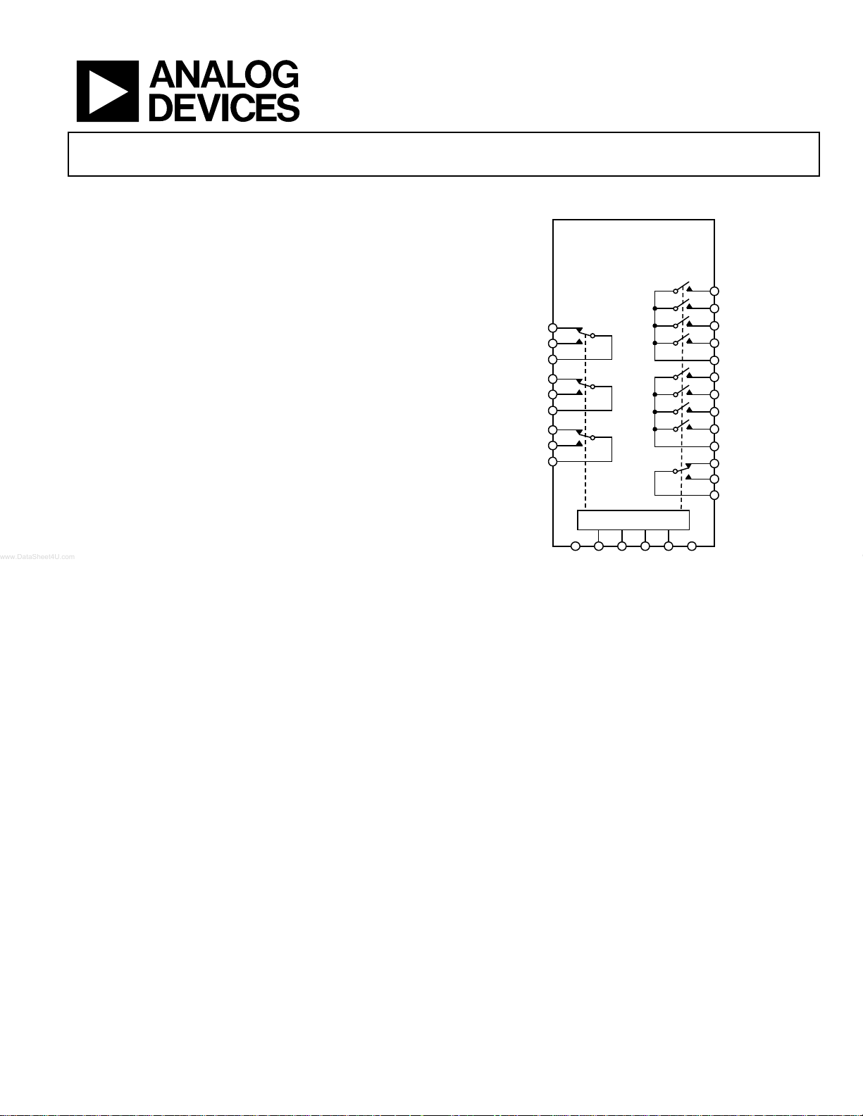
FUNCTIONAL BLOCK DIAGRAM
ADG790
1B
D1
2B
D2
3B
D3
WIDE
BANDWIDTH
SECTION
DD
DECODER
Figure 1.
LOW
DISTORT ION
SECTION
IN3IN2IN1
S/D
S5A
S5B
S5C
S5D
D5
S6A
S6B
S6C
S6D
D6
S4A
S4B
D4
GNDV
6357-001
GENERAL DESCRIPTION
The ADG790 is a single-chip, CMOS switching solution that
comprises four SPDT switches and two 4:1 multiplexers. The
internal architecture of the device provides two switching
sections, a wide bandwidth section and a low distortion section.
The wide bandwidth section contains three SPDT switches that
exhibit low on resistance with excellent flatness and channel
matching. This, combined with wide bandwidth, makes the
three-SPDT-switch configuration ideal for high frequency
signals, such as full speed (12 Mbps) and high speed (480 Mbps)
USB signals and high resolution video signals.
The low distortion section contains a single SPDT switch and
two 4:1 multiplexers that exhibit very low on resistance and
excellent flatness, making these switches ideal for a wide range
of applications, including low distortion audio applications and
low resolution video (CVBS and S-Video) applications.
Rev. 0
Information furnished by Analog Devices is believed to be accurate and reliable. However, no
responsibility is assumed by Anal og Devices for its use, nor for any infringements of patents or ot her
rights of third parties that may result from its use. Specifications subject to change without notice. No
license is granted by implication or otherwise under any patent or patent rights of Analog Devices.
Trademarks and registered trademarks are the property of their respective owners.
All switches conduct equally well in both directions when on
and block signals up to the supply rails when off. A 4-wire
parallel interface controls the operation of the device and
allows the user to control switches from both sections simultaneously. This simplifies the design and provides a cost-effective,
single-chip switching solution for portable devices where
multiple signals share a single port connector. The shutdown
(S/D) pin allows the user to disable all four SPDT switches and
force the 4:1 multiplexers into the S5B and S6B positions,
respectively.
The ADG790 is packaged in a compact, 30-ball WLCSP (6 × 5
2
ball array) with a total area of 7.5 mm
(3 mm × 2.5 mm). This
tiny package size and its low power consumption make the
ADG790 an ideal solution for portable devices.
One Technology Way, P.O. Box 9106, Norwood, MA 02062-9106, U.S.A.
Tel: 781.329.4700 www.analog.com
Fax: 781.461.3113 ©2007 Analog Devices, Inc. All rights reserved.
Page 2

ADG790
TABLE OF CONTENTS
Features.............................................................................................. 1
Test Circuits..................................................................................... 11
Applications....................................................................................... 1
Functional Block Diagram .............................................................. 1
General Description ......................................................................... 1
Revision History ............................................................................... 2
Specifications..................................................................................... 3
Absolute Maximum Ratings............................................................ 5
ESD Caution.................................................................................. 5
Pin Configuration and Function Descriptions............................. 6
Terminology ...................................................................................... 7
Typical Performance Characteristics ............................................. 8
REVISION HISTORY
1/07—Revision 0: Initial Version
Theory of Operation ...................................................................... 13
Wide Bandwidth Section........................................................... 13
Low Distortion Section.............................................................. 13
Control Interface ........................................................................ 13
Evaluation Board............................................................................ 14
Using the ADG790 Evaluation Board ..................................... 14
Outline Dimensions....................................................................... 17
Ordering Guide .......................................................................... 17
Rev. 0 | Page 2 of 20
Page 3

ADG790
SPECIFICATIONS
VDD = 2.7 V to 3.6 V, GND = 0 V, TA = –40°C to +85°C, all switch sections unless otherwise noted.
Table 1.
Parameter Symbol Test Conditions/Comments Min Typ
1
Max Unit
ANALOG SWITCH
Analog Signal Range 0 VDD V
On Resistance RON V
Wide bandwidth section
Low distortion section
On Resistance Flatness R
FLAT(ON)
Wide bandwidth section
Low distortion section
On Resistance Matching
Between Channels
4
∆RON V
Wide bandwidth section
= 2.7 V, VS = 0 V to VDD, IDS = 10 mA (see Figure 18)
DD
2
3
5.9 8.8 Ω
3.9 5.5 Ω
VDD = 2.7 V, VS = 0 V to VDD, IDS = 10 mA (see Figure 18)
2
3
= 2.7 V, VS = 0 V to VDD, IDS = 10 mA
DD
2
2.0 3.6 Ω
0.74 1.6 Ω
0.52 Ω
Low distortion section3 (SPDT) 0.1 Ω
Low distortion section3 (4:1 multiplexers) 0.3 Ω
LEAKAGE CURRENTS
Source Off Leakage IS (OFF)
= 3.6 V, VS = 0 V or 3.6 V, VD = 3.6 V or 0 V
V
DD
(see
Figure 19)
±10 nA
Channel On Leakage ID, IS (ON) VDD = 3.6 V, VS = VD = 0 V or 3.6 V (see Figure 20) ±10 nA
DIGITAL INPUTS (IN1, IN2, IN3, S/D)
Input High Voltage V
Input Low Voltage V
Input High/Input Low Current I
2.0 V
INH
0.8 V
INL
, I
INL
INH
VIN = V
INL
or V
±0.005 ±0.1 μA
INH
Digital Input Capacitance CIN 6 pF
DYNAMIC CHARACTERISTICS
tON t
t
t
OFF
Propagation Delay tD R
Wide bandwidth section
5
R
ON
R
OFF
= 50 Ω, CL = 35 pF, VS = VDD/2 or 0 V (see Figure 24) 20 32 ns
L
= 50 Ω, CL = 35 pF, VS = VDD/2 or 0 V (see Figure 24) 9 15 ns
L
= 50 Ω, CL = 35 pF
L
2
0.3 0.46 ns
Low distortion section3 (SPDT) 0.65 0.95 ns
Low distortion section3 (4:1 multiplexers) 0.4 0.65 ns
Propagation Delay Skew t
Wide bandwidth section
R
SKEW
= 50 Ω, CL = 35 pF
L
2
20 ps
Low distortion section3 (4:1 multiplexers) 40 ps
Break-Before-Make Time Delay t
Charge Injection Q
Wide bandwidth section
Low distortion section
R
BBM
V
INJ
= 50 Ω, CL = 35 pF, VS1 = VS2 = VDD/2 (see Figure 25) 5 11 ns
L
= 0 V, RS = 0 Ω, CL = 1 nF (see Figure 26)
S
2
3
–0.57 pC
6.2 pC
Off Isolation RL = 50 Ω, CL = 5 pF, f = 1 MHz (see Figure 21) –74 dB
Channel-to-Channel Crosstalk RL = 50 Ω, CL = 5 pF, f = 1 MHz (see Figure 22) –77 dB
Total Harmonic Distortion THD + N RL = 32 Ω, f = 20 Hz to 20 kHz, VS = 2 V p-p
Wide bandwidth section
Low distortion section
2
3
1.2 %
0.65 %
–3 dB Bandwidth RL = 50 Ω, CL = 5 pF (see Figure 23)
Wide bandwidth section
2
550 MHz
Low distortion section3 (SPDT) 230 MHz
Low distortion section3 (4:1 multiplexers) 160 MHz
Differential Gain Error CCIR330 test signal
Wide bandwidth section
2
0.07 %
Low distortion section3 (SPDT) 0.08 %
Low distortion section3 (4:1 multiplexers) 0.18 %
Rev. 0 | Page 3 of 20
Page 4
ADG790
Parameter Symbol Test Conditions/Comments Min Typ
1
Max Unit
Differential Phase Error CCIR330 test signal
Wide bandwidth section
2
0.13 Degrees
Low distortion section3 (SPDT) 0.08 Degrees
Low distortion section3 (4:1 multiplexers) 0.19 Degrees
Power Supply Rejection Ratio PSRR f= 10 kHz, no decoupling capacitors –90 dB
Source Off Capacitance CS (OFF) Wide bandwidth section
Low distortion section
Drain Off Capacitance CD (OFF) Wide bandwidth section
2
3
2
3.5 pF
11 pF
5.5 pF
Low distortion section3 (SPDT) 14 pF
Source/Drain On Capacitance CD, CS (ON) Wide bandwidth section
2
8.5 pF
Low distortion section3 (SPDT) 19 pF
Low distortion section3 (4:1 multiplexers) 32 pF
POWER REQUIREMENTS
Supply Voltage VDD 1.65 3.6 V
Supply Current IDD V
1
All typical values are at TA = 25°C, VDD = 3.3 V.
2
Refers to all switches connected to Pin D1, Pin D2, and Pin D3.
3
Refers to all switches connected to Pin D4 (SPDT), Pin D5, and Pin D6 (4:1 multiplexers).
4
Refers to the on resistance matching between the same channels (SxA and SxB, for example) from different multiplexers for the wide bandwidth section and the 4:1
multiplexers from the low distortion section. For the SPDT switch from the low distortion section, it refers to the matching between the S4A and S4B channels.
5
Guaranteed by design; not subject to production test.
= 3.6 V, digital inputs tied to 0 V or 3.6 V 0.1 1 μA
DD
Rev. 0 | Page 4 of 20
Page 5
ADG790
ABSOLUTE MAXIMUM RATINGS
TA = 25°C, unless otherwise noted.
Table 2.
Parameter Rating
VDD to GND –0.3 V to +4.6 V
Analog and Digital Pins1
Peak Current, S or D
Continuous Current, S or D 30 mA
Operating Temperature Range –40°C to +85°C
Storage Temperature Range –65°C to +125°C
Junction Temperature 150°C
Thermal Impedance (θJA)2 80°C/W
Reflow Soldering (Pb Free)
Peak Temperature 260°C (+0°C/–5°C)
Time at Peak Temperature As per JEDEC J-STD-20
1
Overvoltages at IN, S, or D are clamped by internal diodes. Limit current to
the maximum ratings given.
2
Measured with the device soldered on a 4-layer board.
–0.3 V to V
whichever occurs first
100 mA (pulsed at 1 ms, 10%
duty cycle maximum)
+ 0.3 V or 10 mA,
DD
Stresses above those listed under Absolute Maximum Ratings
may cause permanent damage to the device. This is a stress
rating only; functional operation of the device at these or any
other conditions above those indicated in the operational
section of this specification is not implied. Exposure to absolute
maximum rating conditions for extended periods may affect
device reliability.
Only one absolute maximum rating can be applied at any one time.
ESD CAUTION
Rev. 0 | Page 5 of 20
Page 6
ADG790
PIN CONFIGURATION AND FUNCTION DESCRIPTIONS
BALL A1
CORNER
1
234
A
S1A S5A D5 S5C S4A
B
D1 S5B IN1 S5D D4
5
C
S1B GND IN2 V
D
S2B GND IN3 GND S3B
E
D2 S6B S/D S6D D3
F
S2A S6A D6 S6C S3A
TOP VIEW
(BALL SI DE DOWN)
Not to Scale
Figure 2. 30-Ball WLCSP (CB-30-1)
S4B
DD
06357-002
Table 3. Pin Function Descriptions
Ball Name Mnemonic Description
A1 S1A Source Terminal for Mux 1 (Wide Bandwidth Section). Can be an input or an output.
A2 S5A Source Terminal for Mux 5 (Low Distortion Section). Can be an input or an output.
A3 D5 Drain Terminal for Mux 5 (Low Distortion Section). Can be an input or an output.
A4 S5C Source Terminal for Mux 5 (Low Distortion Section). Can be an input or an output.
A5 S4A Source Terminal for Mux 4 (Low Distortion Section). Can be an input or an output.
B1 D1 Drain Terminal for Mux 1 (Wide Bandwidth Section). Can be an input or an output.
B2 S5B Source Terminal for Mux 5 (Low Distortion Section). Can be an input or an output.
B3 IN1 Logic Control Input.
B4 S5D Source Terminal for Mux 5 (Low Distortion Section). Can be an input or an output.
B5 D4 Drain Terminal for Mux 4 (Low Distortion Section). Can be an input or an output.
C1 S1B Source Terminal for Mux 1 (Wide Bandwidth Section). Can be an input or an output.
C2 GND Ground (0 V) Reference.
C3 IN2 Logic Control Input.
C4 VDD Most Positive Power Supply Terminal.
C5 S4B Source Terminal for Mux 4 (Low Distortion Section). Can be an input or an output.
D1 S2B Source Terminal for Mux 2 (Wide Bandwidth Section). Can be an input or an output.
D2 GND Ground (0 V) Reference.
D3 IN3 Logic Control Input.
D4 GND Ground (0 V) Reference.
D5 S3B Source Terminal for Mux 3 (Wide Bandwidth Section). Can be an input or an output.
E1 D2 Drain Terminal for Mux 2 (Wide Bandwidth Section). Can be an input or an output.
E2 S6B Source Terminal for Mux 6 (Low Distortion Section). Can be an input or an output.
E3 S/D Shutdown Logic Control Input.
E4 S6D Source Terminal for Mux 6 (Low Distortion Section). Can be an input or an output.
E5 D3 Drain Terminal for Mux 3 (Wide Bandwidth Section). Can be an input or an output.
F1 S2A Source Terminal for Mux 2 (Wide Bandwidth Section). Can be an input or an output.
F2 S6A Source Terminal for Mux 6 (Low Distortion Section). Can be an input or an output.
F3 D6 Drain Terminal for Mux 6 (Low Distortion Section). Can be an input or an output.
F4 S6C Source Terminal for Mux 6 (Low Distortion Section). Can be an input or an output.
F5 S3A Source Terminal for Mux 3 (Wide Bandwidth Section). Can be an input or an output.
Rev. 0 | Page 6 of 20
Page 7

ADG790
TERMINOLOGY
IDD
Positive supply current.
V
(VS)
D
Analog voltage on Terminal D and Terminal S.
R
ON
Ohmic resistance between Terminal D and Terminal S.
R
FLAT (ON)
Flatness is defined as the difference between the maximum and
minimum value of on resistance as measured.
ΔR
ON
On resistance match between any two channels.
I
(OFF)
S
Source leakage current with the switch off.
I
, IS (ON)
D
Channel leakage current with the switch on.
V
INL
Maximum input voltage for Logic 0.
V
INH
Minimum input voltage for Logic 1.
I
(I
)
INL
INH
Input current of the digital input.
C
(OFF)
S
Off switch source capacitance. Measured with reference
to ground.
, CS (ON)
C
D
On switch capacitance. Measured with reference to ground.
C
IN
Digital input capacitance.
t
ON
Delay time between the 50% and the 90% points of the digital
input and switch on condition.
t
OFF
Delay time between the 50% and the 10% points of the digital
input and switch off condition.
t
BBM
On or off time measured between the 80% points of both
switches when switching from one to the other.
t
D
Signal propagation delay through the switch measured
between the 50% points of the input signal and its corresponding output signal.
t
SKEW
Difference in propagation delay between the selected inputs on
the 4:1 multiplexers or any two SPDT switches from the wide
bandwidth section.
Charge Injection
A measure of the glitch impulse transferred from the digital
input to the analog output during on-off switching.
Off Isolation
A measure of unwanted signal coupling through an off switch.
Crosstalk
A measure of unwanted signal that is coupled through from one
channel to another as a result of parasitic capacitance.
−3 dB Bandwidth
The frequency at which the output is attenuated by 3 dB.
Insertion Loss
The loss due to the on resistance of the switch.
THD + N
The ratio of the harmonic amplitudes plus signal noise to the
fundamental.
Differential Gain Error
The measure of how much color saturation shift occurs when
the luminance level changes. Both attenuation and amplification
can occur; therefore, the largest amplitude change between any
two levels is specified and expressed in percent.
Differential Phase Error
The measure of how much hue shift occurs when the luminance
level changes. It can be a negative or a positive value and is
expressed in degrees of subcarrier phase.
Rev. 0 | Page 7 of 20
Page 8

ADG790
TYPICAL PERFORMANCE CHARACTERISTICS
7.5
TA = 25°C
I
= 10mA
DS
7.0
6.5
6.0
()
ON
R
5.5
5.0
4.5
4.0
VDD = 2.7V
VDD = 3.3V
VDD = 3.6V
VS (V)
Figure 3. On Resistance vs. Source Voltage,
Wide Bandwidth Section
6.5
VDD = 3.3V
I
= 10mA
DS
6.0
5.5
()
ON
R
5.0
4.5
4.0
0 0.5 1.0 1.5 2.0 2.5 3.0
TA = +25°C
TA = +85°C
TA = –40°C
VS (V)
Figure 4. On Resistance vs. Temperature,
Wide Bandwidth Section
06357-039
3.53.02.52.01.51.00.50
06357-040
4.5
4.3
4.1
3.9
3.7
()
3.5
ON
R
3.3
3.1
2.9
2.7
2.5
0 0.5 1.0 1.5 2.0 2.5 3.0
TA = –40°C
TA = +85°C
TA = +25°C
VS (V)
Figure 6. On Resistance vs. Temperature,
Low Distortion Section
20
18
16
14
(ns)
OFF
12
t
/
ON
t
10
8
6
4
–40 –20 0 20 40 60 80
Figure 7. t
t
OFF
t
ON
TEMPERATURE (°C)
Times vs. Temperature
ON/tOFF
VDD = 3.3V
T
R
C
VDD = 3.3V
I
= 10mA
DS
= 25°C
A
= 50
L
= 35pF
L
06357-042
06357-028
TA = 25°C
I
4.5
4.0
()
ON
3.5
R
3.0
2.5
VDD = 2.7V
VDD = 3.3V
VS (V)
= 10mA
DS
VDD = 3.6V
06357-041
3.53.02.52.01.51.00.50
Figure 5. On Resistance vs. Source Voltage,
Low Distortion Section
–1
VDD = 3.3V
–3
T
= 25°C
A
–5
–7
–9
ATTENUATI ON (dB)
–11
–13
–15
0.01 1000
0.1 1 10 100
WIDE BANDWI DTH SECTIO N
LOW DISTORTION SECTION
FREQUENCY (M Hz)
Figure 8. On Response vs. Frequency,
Low Distortion Section (SPDT)
06357-029
Rev. 0 | Page 8 of 20
Page 9

ADG790
–
–
0
–2
VDD = 3.3V
–4
= 25°C
T
A
–6
–8
–10
–12
ATTENUATION (dB)
–14
–16
–18
–20
0.01 1000
0.1 1 10 100
FREQUENCY (M Hz)
Figure 9. On Response vs. Frequency,
06357-030
10
VDD = 3.3V
= 25°C
T
A
–20
WIDE BANDWI DTH AND LOW
DISTORT ION SECT IONS
–30
–40
–50
–60
–70
ATTENUATION (dB)
–80
–90
–100
–110
0.001 0.01 0.1 1 10 100
0.0001 1000
FREQUENCY (MHz)
Figure 12. Off Isolation vs. Frequency
06357-033
Low Distortion Section (4:1 Multiplexers)
20
VDD = 3.3V
= 25°C
T
A
–30
WIDE BANDWIDT H AND
LOW DISTORTION SECTIONS
–40
INPUT SIG NAL = 0dBm
DC BIAS = 0.5V
–50
–60
–70
–80
ATTENUATION (dB)
–90
–100
–110
06357-034
X = 20ns/DIV Y = 835mV/DIV
Figure 10. USB 1.1 Eye Diagram
06357-021
–120
0.001 0.01 0.1 1 10 100
0.0001 1000
FREQUENCY (MHz)
Figure 13. Crosstalk vs. Frequency
X = 250ps/DIV Y = 100mV/DIV
Figure 11. USB 2.0 Eye Diagram
06357-022
Rev. 0 | Page 9 of 20
1.3
1.2
1.1
1.0
0.9
THD + N (%)
0.8
0.7
0.6
0.5
10 100000
WIDE BANDWI DTH SECTI ON
VDD = 3.3V
R
L
V
S
T
A
DC BIAS = 1.65V
LOW DISTORTION SECTION
100 1000 10000
FREQUENCY (Hz)
= 32
= 2V p-p
= 25°C
Figure 14. THD + N vs. Frequency
06357-035
Page 10

ADG790
500
450
400
350
300
250
(µA)
DD
I
200
150
100
50
0
0 0.5 1.0 1.5 2.0 2.5 3.0
VIN (V)
Figure 15. Supply Current vs. Input Logic Level
8
7
6
5
4
(pC)
INJ
3
Q
VDD = 3.3V
C
= 1nF
2
L
T
= 25°C
A
1
0
–1
0 0.5 1.0 1.5 2.0 2.5 3.0
LOW DISTORTION
WIDE BANDWI DTH
VS (V)
SECTION
SECTION
Figure 16. Charge Injection vs. Source Voltage
VDD = 3.3V
= 25°C
T
A
06357-036
06357-037
0
VDD = 3.3V
T
= 25°C
A
WIDE BANDWI DTH AND LOW
–20
DISTORTION SECTIONS.
0dBm SIGNAL SUPERIMPO SED
ON SUPPLY VOLTAGE.
–40
NO DECOUPLI NG CAPACITO RS
USED.
–60
PSRR (dB)
–80
–100
–120
0.0001 1000
0.001 0.01 0.1 1 10 100
FREQUENCY (M Hz)
Figure 17. Power Supply Rejection Ratio vs. Frequency
06357-038
Rev. 0 | Page 10 of 20
Page 11

ADG790
V
V
V
V
TEST CIRCUITS
I
DS
V1
SD
V
S
RON = V1/I
DS
Figure 18. On Resistance
IS (OFF) ID (OFF)
SD
A A
S
Figure 19. Off Leakage
NC
SD
NC = NO CONNECT
Figure 20. On Leakage
ID (ON)
A
V
DD
0.1µF
NETWO RK
ANALYZER
V
OUT
06357-003
CHANNEL-TO- CHANNEL CROSST ALK = 20 lo g
R
50
50
V
L
S
SxA
SxB
GND
V
V
OUT
V
DD
Dx
R
L
50
S
6357-010
Figure 22. Channel-to-Channel Crosstalk
SxB
0.1µF
DD
V
DD
GND
SxA
Dx
V
WITH SWITCH
OUT
WITHOUT SWITCH
V
OUT
NETWORK
ANALYZER
50
V
V
OUT
R
L
50
S
06357-011
V
D
06357-004
D
6357-005
INSERTION LOSS = 20 log
Figure 23. –3 dB Bandwidth
NC
OFF I SOLATI ON = 20 log
NC = NO CONNECT
SxB
0.1µF
DD
V
DD
SxA
Dx
GND
V
OUT
V
50
S
Figure 21. Off Isolation
NETWORK
ANALYZER
50
V
S
V
OUT
R
L
50
6357-009
Rev. 0 | Page 11 of 20
Page 12

ADG790
V
VDDV
V
DD
0.1µF
V
V
DD
SxA
V
S
SxB
INx
GND
Dx
R
L
50
V
C
L
35pF
OUT
Figure 24. Switching Times (t
0.1µF
V
DD
SxA
S
SxB
INx
GND
Dx
R
L
50
V
C
L
35pF
OUT
Figure 25. Break-Before-Make Time Delay (t
DD
0.1µF
IN
V
OUT
, t
ON
V
IN
0V
V
S
V
OUT
t
BBM
50% 50%
t
ON
)
OFF
50% 50%
)
BBM
90%
10%
80% 80%
t
t
OFF
BBM
6357-006
6357-007
Dx
V
S
INx
NC = NO CONNECT
V
DD
GND
SxA
SxB
C
1nF
NC
V
OUT
L
SxB TO Dx ON
V
IN
V
OUTVOUT
SxB TO Dx OFF
Q
= CL× V
INJ
OUT
06357-008
Figure 26. Charge Injection
Rev. 0 | Page 12 of 20
Page 13

ADG790
THEORY OF OPERATION
The ADG790 is a single-chip, CMOS switching solution that
comprises four SPDT switches and two 4:1 multiplexers. The
internal architecture used by the device groups the switches into
two sections, each optimized to provide the best performance in
terms of bandwidth and distortion. The on-chip parallel
interface controls the operation of all switches, allowing the
user to control switches from both sections simultaneously.
WIDE BANDWIDTH SECTION
The wide bandwidth section contains three SPDT switches
S1A/S1B-D1, S2A/S2B-D2, and S3A/S3B-D3. These switches
use a CMOS topology that ensures, besides low on resistance
and excellent flatness, the ability to switch signals up to the
supply rails. This, combined with the low switch capacitance,
provides the wide bandwidth required when switching high
frequency signals. The three SPDT switches are also optimized
to provide low propagation delay and excellent matching
between the channels, making the ADG790 ideal for applications that use multiple signals, such as universal USB switches
(full and high speed), or RGB video signals, such as VGA.
LOW DISTORTION SECTION
The low distortion section contains a single SPDT switch
(S4A/S4B-D4) and two 4:1 multiplexers (S5A/S5B/S5C/S5D-D5
and S6A/S6B/S6C/S6D-D6, respectively). The switches from
this section also use a CMOS topology that exhibits very low on
resistance and flatness while maintaining a wide bandwidth that
makes them suitable for a wide range of applications, including
low distortion audio and standard definition video signals. The
channels from the 4:1 multiplexers are matched to provide
optimal performance when used with differential signals such
as S-Video.
CONTROL INTERFACE
The operation of the ADG790 is controlled via a 4-wire parallel
interface. The logic levels applied to the IN1, IN2, and IN3 pins
control the operation of the switches from both the wide bandwidth and low distortion sections, as shown in
shutdown pin (S/D) allows the user to disable all four SPDT
switches and force the 4:1 multiplexers into the S5B and S6B
positions, respectively. This function can be used to set up a low
speed communication protocol between the circuitry from both
sides of the device, which allows automatic configuration of the
switching function.
For example, in modern handset applications, where a single
connector is used as a multifunction communication port, the
S5B-D5 and S6B-D6 configuration obtained by setting the S/D
pin high can be used to detect the type of peripheral device
connected to the handset. The ADG790 then automatically routes
the required signals to the communication port connector.
Tabl e 4 . The
Table 4. Truth Table
Logic Control Inputs Switch Status
S1A-D1
S2A-D2
S3A-D3
S5D-D5
S/D IN1 IN2 IN3
1 X
0 0 0 0 Off On Off On Off Off On
0 0 0 1 On Off On Off Off Off Off
0 0 1 0 Off On On Off Off On Off
0 0 1 1 Off On On Off Off Off On
0 1 0 0 Off On On Off On Off Off
0 1 0 1 On Off Off On Off Off Off
0 1 1 0 Off On Off On On Off Off
0 1 1 1 Off On Off On Off On Off
1
X = logic state doesn’t matter.
1
1
X
X
S6D-D6
1
Off Off Off Off Off On Off
S1B-D1
S2B-D2
S3B-D3
S4A-D4 S4B-D4
S5A-D5
S6A-D6
S5B-D5
S6B-D6
S5C-D5
S6C-D6
Rev. 0 | Page 13 of 20
Page 14

ADG790
EVALUATION BOARD
The ADG790 evaluation board allows designers to evaluate the
high performance of the device with a minimum of effort.
The EVAL-ADG790 includes a printed circuit board populated
with the ADG790; it can be used to evaluate the performance of
the device. It interfaces to the USB port of a PC, allowing the user
to easily program the ADG790 through the USB port using the
software provided with the board. Schematics of the evaluation
board are shown in
on any PC that has Microsoft® Windows® 2000 or Windows®
XP installed.
Figure 27 and Figure 28. The software runs
USING THE ADG790 EVALUATION BOARD
The ADG790 evaluation board is a test system designed to
simplify the evaluation of the device. Each input/output of the
part comes with a standardized socket to allow connection to
and from USB, CVBS, S-Video, and VGA signal sources. A data
sheet for the ADG790 evaluation board is also available with
full information on setup and operation.
Rev. 0 | Page 14 of 20
Page 15

ADG790
C19
10µF
06357-013
+
GREEN
DVDD
ADP3303AR-3.3
126
OUT
OUT
ININSD
875
C17
0.1µF
3
NR
ERR
U4
4
GND
C16
0.1µF
C15
+
R10
10µF
D1
1k
5V USB
54321
IO
D–
D+
GND
R9
2.2k
VBUS
J14
USB-MINI-B
R8
2.2k
SHIELD
DVDD
DVDD DVDD DVDD
C14
0.1µF
DVDD
C4
R6
0
2.2µF
+
C3
0.1µF
876
5
CC
WP
V
SCL
SDA
U3
A0A1A2
123
SS
V
4
24LC64
DVDD
A0
A1A2A3
8
9
15
16
PD1/FD9
PD2/FD10
CTL0/*FLAGA
CTL1/*FLAGB
30
PD5/FD13
PD4/FD12
PD3/FD11
CTL2/*FLAGC
31
525150494847464525242322212019
SDA
PD7/FD15
PD6/FD14
PA2/*SLOE
PA3/*WU2
PA4/FIF OADR0
PA5/FIF OADR1
PA0/INT0
PA1/INT1
33343536373839
SCL
DPLUS
DMINUS
PA6/*PKTEND
PA7/*FLAGD/SLCS
RDY0/*SLRD
RDY1/*SLW R
1
2
40
18
U2
CY7C68013-56LFC
55
PB2/FD2
PB1/FD1
PB0/FD0
43
32
VCC
27
17
11
7
3
AVCC
424454
PB4/FD4
PB3/FD3
RESET
*WAKEUP
PD0/FD8
PB7/FD7
PB6/FD6
PB5/FD5
CLKOUT
29
C13
12pF
Y1
24MHz
C12
12pF
5
4
56
53
XTALIN
XTALOUT
IFCLK
13
41
GND
28
26
12
10
6
AGND
RESERVED
14
R7
10k
DVDD
C11
C10
C9
C8
C7
C6
C5
0.1µF
0.1µF
0.1µF
0.1µF
0.1µF
0.1µF
0.1µF
DVDD
DVDD
R5
100k
C2
0.1µF
R4
100k
C1
10µF
+
Figure 27. EVAL-ADG790 Schematic
USB Controller Section
Rev. 0 | Page 15 of 20
Page 16

ADG790
J13-4
J13-5
J13-6
J13-7
J13-3
J13-2
J13-1
T23
T22
T21
VGA R_O
VGA B_O
VGA G_O
J13-13
J13-14
T25
T24
VSYNC_O
HSYNC_O
J13-8
GND
1
J8
2
PHONO_DUAL
3
TOP
BOTTOM
T27
GND
1
T26
T28
PHONO_DUAL
T29
GND
1
J9
2
3
PHONO_DUAL
J10
2
TOP
BOTTOM
T31
T30
06357-014
GND
1
3
TOP
BOTTOM
J5
TX_O
IO1_O
IO2_O
USB2.OID/VGAR_O
USB2.OD+/VG AB_O
USB2.OD–/VG AG_O
IO1/VGAH/S-VI DEOY/TX_O
IO1/VGAV/S-VIDEOC/RX_O
J11
USB
DD
V
D–D+GNDSHSH
12345
6
USB2.OID
T19
T18
3
PHONO_DUAL
2
TOP
BOTTOM
T20
T32
IO2/VGAV/S-VIDEOC/RX_O
VBUS
USBID_I
RX_O
IO1/VGAH/S-VIDEOY/TX_O
IO1/VGAH/S-VIDEOY/TX_O
IO2/VGAV/S-VIDEOC/RX_O
1
CVBS_O
MIC_O
MIC/CVBS_O
MIC/CVBS_O
34
USB2.OID/VGAR_O
USB2.OD+/VG AB_O
USB2.OD–/VG AG_O
DVDD
B1E1E5B5A3
D1D2D3D4D5
DD
V
C4
GND
D4
GND
D2
GND
C2
T33
S1A
A1
C1F1D1F5D5A5C5A2B2A4B4
IO1/VGAH/S-VIDEOY/TX_O
USB2.OD+/VG AB_O
IO2/VGAV/S-VIDEOC/RX_O
USB2.OID/VGAR_O
MIC/CVBS_O
F3
D6
S2A
S3A
S4A
S1B
S2B
S5A
S3B
S4B
USB2.OD–/VGAG_O
SVIDEOC_I
S/DIN3IN2IN1
A0A1A2A3
E3D3B3 C3
SVIDEOY_I
T16
U1
R3
ADG790
S5C
S6A
S6C
S5B
S5D
F2E2F4
S6D
S6B
E4
T15
T14
75
R2
75
T17
J12 MINI-DIN-4
432
SVIDEOY_O
SVIDEOC_O
2
1
432
VGAR_I
USBID_I
CVBS_I
VGAB_I
VGAG_I
USB2.OD–_I
USB2.OD+_I
TX_I
MIC_I
IO1_I
RX_I
IO2_I
VGAH_I
SVIDEOY_I
VGAV_I
SVIDEOC_I
1
2
43
IO1/VGAH/S-VI DEOY/TX_O
1
IO2/VGAV/S-VIDEOC/RX_O
J6 MINI-DIN-4
IO1_I
IO2_I
T1 T3
TOP
BOTTOM
3
2
J1
1
PHONO_DUAL
GND
TX_I
RX_I
R1
75
T2 T4
3
J2
PHONO_DUAL
T5 T6
TOP
BOTTOM
2
1
PHONO_DUAL
GND
MIC_I
CVBS_I
VGAR_I
VGAG_I
VGAB_I
VBUS
USB2.OD–_I
USB2.OD+_I
TOP
BOTTOM
3
2
T7 T8
12345
DD
D–
D+
J3
1
V
GND
SH
GND
J4
USB
T11
T10
T9
6
SH
J7-1
J7-2
J7-3
VGAH_I
VGAV_I
T13
T12
J7-4
J7-5
J7-6
J7-7
J7-13
J7-14
J7-8
Figure 28. EVAL-ADG790 Schematic
Switch Section
Rev. 0 | Page 16 of 20
Page 17

ADG790
OUTLINE DIMENSIONS
0.65
2.56
2.50
2.44
BALL A1
CORNER
TOP VIEW
(BALL SI DE DOWN)
3.06
3.00
2.94
Figure 29. 30-Ball Wafer Level Chip Scale Package [WLCSP]
Dimensions shown in millimeters
ORDERING GUIDE
Model Temperature Range Package Description Package Option
ADG790BCBZ-REEL
EVAL-ADG790EBZ
1
Z = Pb-free part.
1
1
–40°C to +85°C 30-Ball Wafer Level Chip Scale Package [WLCSP] CB-30-1
Evaluation Board
0.59
0.53
0.28
0.24
0.20
(CB-30-1)
SEATING
PLANE
0.50
BALL P ITCH
0.36
0.32
0.28
BOTTOM VIEW
(BALL SI DE UP)
12345
A
B
C
D
E
F
092106- A
Rev. 0 | Page 17 of 20
Page 18

ADG790
NOTES
Rev. 0 | Page 18 of 20
Page 19

ADG790
NOTES
Rev. 0 | Page 19 of 20
Page 20

ADG790
NOTES
©2007 Analog Devices, Inc. All rights reserved. Trademarks and
registered trademarks are the property of their respective owners.
D06357-0-1/07(0)
Rev. 0 | Page 20 of 20
 Loading...