Analog Devices ADG784 Datasheet

CMOS 3 V/5 V, Wide Bandwidth Quad 2:1
a
FEATURES
Low Insertion Loss and On Resistance: 4 Typical
On-Resistance Flatness <2
Bandwidth >200 MHz
Single 3 V/5 V Supply Operation
Rail-to-Rail Operation
Very Low Distortion: <1%
Low Quiescent Supply Current (100 nA Typical)
Fast Switching Times
10 ns
t
ON
t
4 ns
OFF
TTL/CMOS Compatible
For Functionally Equivalent Devices in 16-Lead QSOP/
SOIC Packages, See ADG774
APPLICATIONS
100VG-AnyLAN
Token Ring 4 Mbps/16 Mbps
ATM25/155
NIC Adapter and Hubs
Audio and Video Switching
Relay Replacement
Mux in Chip Scale Package
ADG784
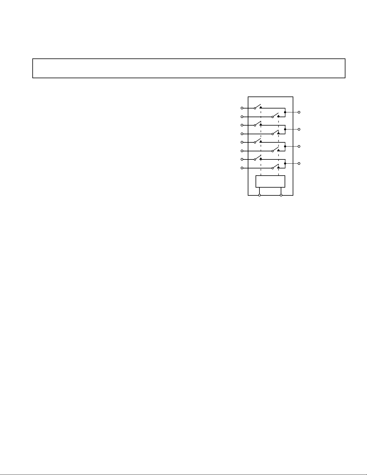
FUNCTIONAL BLOCK DIAGRAM
ADG784
S1A
S1B
S2A
S2B
S3A
S3B
S4A
S4B
1-OF-2
DECODER
EN
IN
D1
D2
D3
D4
GENERAL DESCRIPTION
The ADG784 is a monolithic CMOS device comprising four
2:1 multiplexer/demultiplexers with high impedance outputs.
The CMOS process provides low power dissipation yet gives
high switching speed and low on resistance. The on-resistance
variation is typically less than 0.5 Ω with an input signal ranging
from 0 V to 5 V.
The bandwidth of the ADG784 is greater than 200 MHz and
this, coupled with low distortion (typically 0.5%), makes the
part suitable for switching fast ethernet signals.
The on-resistance profile is very flat over the full analog input
range ensuring excellent linearity and low distortion when switching audio signals. Fast switching speed, coupled with high signal
bandwidth, also makes the parts suitable for video signal switching. CMOS construction ensures ultralow power dissipation
making the parts ideally suited for portable and battery powered
instruments.
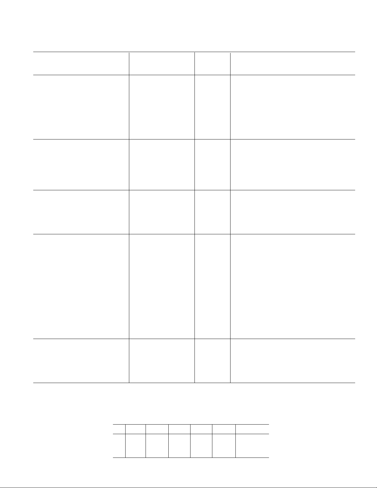
The ADG784 operates from a single 3.3 V/5 V supply and is
TTL logic compatible. The control logic for each switch is shown
in the Truth Table.
These switches conduct equally well in both directions when
ON, and have an input signal range that extends to the supplies. In the OFF condition, signal levels up to the supplies
are blocked. The ADG784 switches exhibit break-beforemake switching action.
PRODUCT HIGHLIGHTS
1. Also Available as ADG774 in 16-Lead QSOP and SOIC.
2. Wide Bandwidth Data Rates >200 MHz.
3. Ultralow Power Dissipation.
4. Extended Signal Range.
The ADG784 is fabricated on a CMOS process giving an
increased signal range that fully extends to the supply rails.
5. Low Leakage over Temperature.
6. Break-Before-Make Switching.
This prevents channel shorting when the switches are configured as a multiplexer.
7. Crosstalk is typically –70 dB @ 30 MHz.
8. Off isolation is typically –60 dB @ 10 MHz.
9. Available in Chip Scale Package (CSP).
REV. 0
Information furnished by Analog Devices is believed to be accurate and
reliable. However, no responsibility is assumed by Analog Devices for its
use, nor for any infringements of patents or other rights of third parties that
may result from its use. No license is granted by implication or otherwise
under any patent or patent rights of Analog Devices.
One Technology Way, P.O. Box 9106, Norwood, MA 02062-9106, U.S.A.
Tel: 781/329-4700 www.analog.com
Fax: 781/326-8703 © Analog Devices, Inc., 2001

ADG784–SPECIFICATIONS
SINGLE SUPPLY
(VDD = 5 V 10%, GND = 0 V. All specifications T
MIN
to T
unless otherwise noted.)
MAX
B Version
to
T
Parameter 25CT
MIN
MAX
Unit Test Conditions/Comments
ANALOG SWITCH
Analog Signal Range 0 V to V
On Resistance (R
) 2.2 Ω typ VD = 0 V to VDD, IS = –10 mA
ON
DD
V
5 Ω max
On Resistance Match Between
Channels (∆R
)0.15 Ω typ VD = 0 V to VDD, IS = –10 mA
ON
0.5 Ω max
On Resistance Flatness (R
FLAT(ON)
) 0.5 Ω typ VD = 0 V to VDD; IS = –10 mA
1 Ω max
LEAKAGE CURRENTS
Source OFF Leakage IS (OFF) ± 0.01 nA typ VD = 4.5 V, VS = 1 V; VD = 1 V, VS = 4.5 V;
± 0.5 ± 1 nA max Test Circuit 2
Drain OFF Leakage I
(OFF) ± 0.01 nA typ VD = 4.5 V, VS = 1 V; VD = 1 V, VS = 4.5 V;
D
± 0.5 ± 1 nA max Test Circuit 2
Channel ON Leakage I
, IS (ON) ±0.01 nA typ VD = VS = 4.5 V; VD = VS = 1 V; Test Circuit 3
D
± 0.5 ± 1 nA max
DIGITAL INPUTS
Input High Voltage, V
Input Low Voltage, V
INL
INH
2.4 V min
0.8 V max
Input Current
I
INL
or I
INH
0.001 µA typ VIN = V
INL
or V
INH
± 0.5 µA max
DYNAMIC CHARACTERISTICS
t
ON
t
OFF
Break-Before-Make Time Delay, t
Off Isolation –65 dB typ R
Channel-to-Channel Crosstalk –75 dB typ R
Bandwidth –3 dB 240 MHz typ R
Distortion 0.5 % typ R
Charge Injection 10 pC typ C
C
(OFF) 10 pF typ f = 1 kHz
S
(OFF) 20 pF typ f = 1 kHz
C
D
2
10 ns typ RL = 100 Ω, CL = 35 pF,
20 ns max V
= 3 V; Test Circuit 4
S
4 ns typ RL = 100 Ω, CL = 35 pF,
8 ns max V
D
5 ns typ RL = 100 Ω, CL = 35 pF,
1 ns min V
= 3 V; Test Circuit 4
S
= VS2 = 5 V; Test Circuit 5
S1
= 100 Ω, f = 10 MHz; Test Circuit 7
L
= 100 Ω, f = 10 MHz; Test Circuit 8
L
= 100 Ω; Test Circuit 6
L
= 100 Ω
L
= 1 nF; Test Circuit 9
L
CD, CS (ON) 30 pF typ f = 1 MHz
POWER REQUIREMENTS V
I
DD
1 µA max
= 5.5 V
DD
Digital Inputs = 0 V or V
DD
0.001 µA typ
I
IN
I
O
NOTES
1
Temperature ranges are as follows: B Version, –40°C to +85°C.
2
Guaranteed by design, not subject to production test.
Specifications subject to change without notice.
1 µA typ VIN = 5 V
100 mA max VS/VD = 0 V
–2–
REV. 0

ADG784
SINGLE SUPPLY
(VDD = 3 V 10%, GND = 0 V. All specifications T
MIN
to T
unless otherwise noted.)
MAX
B Version
T
to
Parameter 25CT
MIN
MAX
Unit Test Conditions/Comments
ANALOG SWITCH
Analog Signal Range 0 V to V
On Resistance (R
)4 Ω typ VD = 0 V to VDD, IS = –10 mA
ON
DD
V
10 Ω max
On Resistance Match Between
Channels (∆R
)0.15 Ω typ VD = 0 V to VDD, IS = –10 mA
ON
0.5 Ω max
On Resistance Flatness (R
FLAT(ON)
) 2Ω typ VD = 0 V to VDD, IS = –10 mA
4 Ω max
LEAKAGE CURRENTS
Source OFF Leakage I
(OFF) ± 0.01 nA typ VD = 3 V, VS = 1 V; VD = 1 V, VS = 3 V;
S
± 0.5 ± 1 nA max Test Circuit 2
Drain OFF Leakage I
(OFF) ± 0.01 nA typ VD = 3 V, VS = 1 V; VD = 1 V, VS = 3 V;
D
± 0.5 ± 1 nA max Test Circuit 2
Channel ON Leakage I
, IS (ON) ±0.01 nA typ VD = VS = 3 V; VD = VS = 1 V; Test Circuit 3
D
± 0.5 ± 1 nA max
DIGITAL INPUTS
Input High Voltage, V
Input Low Voltage, V
INL
INH
2.0 V min
0.4 V max
Input Current
I
INL
or I
INH
0.001 µA typ VIN = V
± 0.5 µA max
DYNAMIC CHARACTERISTICS
t
ON
t
OFF
Break-Before-Make Time Delay, t
Off Isolation –65 dB typ R
Channel-to-Channel Crosstalk –75 dB typ R
Bandwidth –3 dB 240 MHz typ R
Distortion 2 % typ R
Charge Injection 3 pC typ C
(OFF) 10 pF typ f = 1 kHz
C
S
C
(OFF) 20 pF typ f = 1 kHz
D
2
12 ns typ RL = 100 Ω, CL = 35 pF,
25 ns max V
= 1.5 V; Test Circuit 4
S
5 ns typ RL = 100 Ω, CL = 35 pF,
10 ns max V
D
5 ns typ RL = 100 Ω, CL = 35 pF,
1 ns min V
= 1.5 V; Test Circuit 4
S
= VS2 = 3 V; Test Circuit 5
S1
= 50 Ω, f = 10 MHz; Test Circuit 7
L
= 50 Ω, f = 10 MHz; Test Circuit 8
L
= 50 Ω; Test Circuit 6
L
= 50 Ω
L
= 1 nF; Test Circuit 9
L
CD, CS (ON) 30 pF typ f = 1 MHz
POWER REQUIREMENTS V
= 3.3 V
DD
Digital Inputs = 0 V or V
I
DD
1 µA max
0.001 µA typ
I
IN
I
O
NOTES
1
Temperature ranges are as follows: B Version, –40°C to +85°C.
2
Guaranteed by design, not subject to production test.
Specifications subject to change without notice.
1 µA typ VIN = 3 V
100 mA max VS/VD = 0 V
INL
or V
INH
DD
REV. 0
Table I. Truth Table
EN IN D1 D2 D3 D4 Function
1 X Hi-Z Hi-Z Hi-Z Hi-Z DISABLE
0 0 S1A S2A S3A S4A IN = 0
0 1 S1B S2B S3B S4B IN = 1
–3–
 Loading...