ANALOG DEVICES ADG781 Service Manual

2.5 Quad SPST Switches
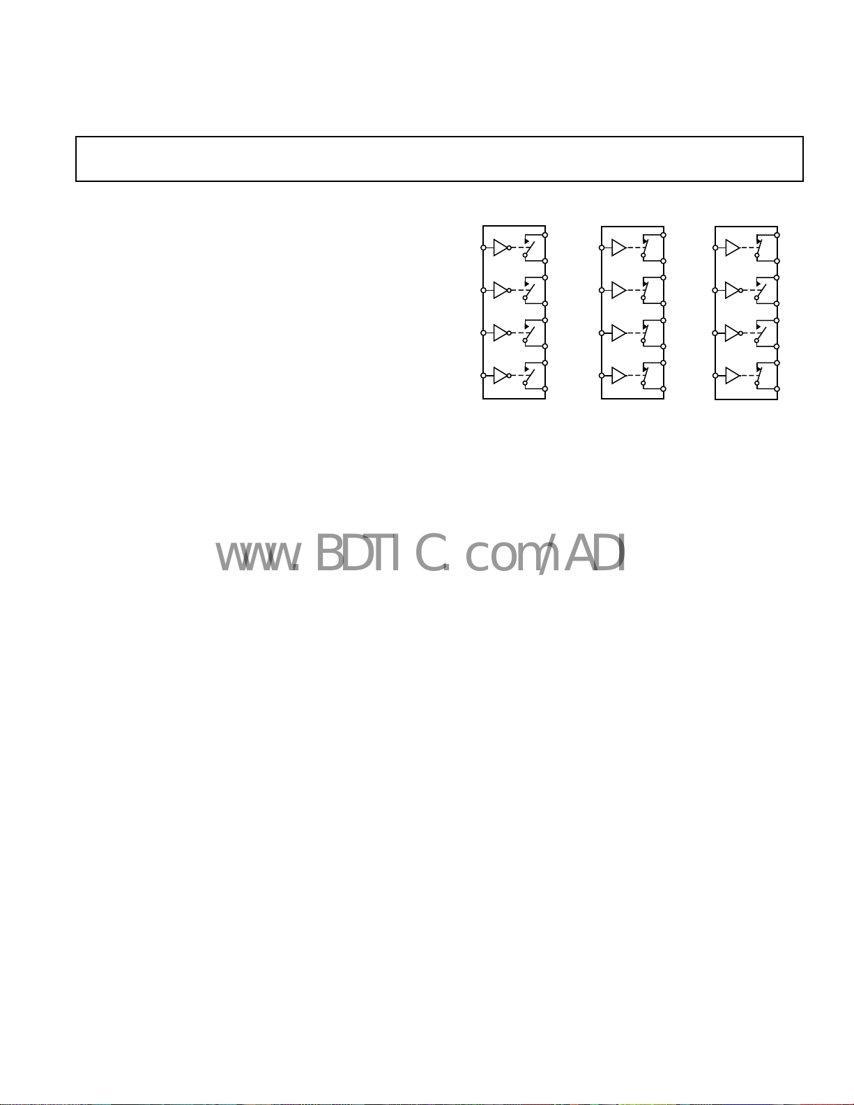
IN1
IN2
IN3
IN4
S1
D1
S2
D2
S3
D3
S4
D4
ADG781
SWITCHES SHOWN FOR A LOGIC “1” INPUT
IN1
IN2
IN3
IN4
S1
D1
S2
D2
S3
D3
S4
D4
ADG782
IN1
IN2
IN3
IN4
S1
D1
S2
D2
S3
D3
S4
D4
ADG783
www.BDTIC.com/ADI
a
FEATURES
1.8 V to 5.5 V Single Supply
Low On Resistance (2.5 Typ)
Low On-Resistance Flatness (0.5 )
–3 dB Bandwidth > 200 MHz
Rail-to-Rail Operation
20-Lead 4 mm 4 mm Chip Scale Package
Fast Switching Times
= 16 ns
t
ON
t
= 10 ns
OFF
Typical Power Consumption (< 0.01 W)
TTL/CMOS Compatible
For Functionally Equivalent Devices in 16-Lead TSSOP
and SOIC Packages, See ADG711/ADG712/ADG713
APPLICATIONS
Battery Powered Systems
Communication Systems
Sample Hold Systems
Audio Signal Routing
Video Switching
Mechanical Reed Relay Replacement
in Chip Scale Package
ADG781/ADG782/ADG783
FUNCTIONAL BLOCK DIAGRAMS
GENERAL DESCRIPTION
The ADG781, ADG782, and ADG783 are monolithic CMOS
devices containing four independently selectable switches. These
switches are designed on an advanced submicron process that
provides low power dissipation and high switching speed, low on
resistance, low leakage currents and high bandwidth.
They are designed to operate from a single 1.8 V to 5.5 V supply, making them ideal for use in battery powered instruments
and with the new generation of DACs and ADCs from Analog
Devices. Fast switching times and high bandwidth make the
part suitable for video signal switching.
The ADG781, ADG782, and ADG783 contain four independent
single-pole/single throw (SPST) switches. The ADG781 and
ADG782 differ only in that the digital control logic is inverted.
The ADG781 switches are turned on with a logic low on the
appropriate control input, while a logic high is required to turn
on the switches of the ADG782. The ADG783 contains two
switches whose digital control logic is similar to the ADG781,
while the logic is inverted on the other two switches.
Each switch conducts equally well in both directions when ON.
The ADG783 exhibits break-before-make switching action.
The ADG781/ADG782/ADG783 are available in 20-lead chip
scale packages.
REV. A
Information furnished by Analog Devices is believed to be accurate and
reliable. However, no responsibility is assumed by Analog Devices for its
use, nor for any infringements of patents or other rights of third parties that
may result from its use. No license is granted by implication or otherwise
under any patent or patent rights of Analog Devices.
PRODUCT HIGHLIGHTS
1. 20-Lead 4 mm ⫻ 4 mm Chip Scale Package (CSP).
2. 1.8 V to 5.5 V Single Supply Operation. The ADG781,
ADG782, and ADG783 offer high performance and are
fully specified and guaranteed with 3 V and 5 V supply
rails.
3. Very Low R
voltage of 1.8 V, R
(4.5 Ω max at 5 V, 8 Ω max at 3 V). At supply
ON
is typically 35 Ω over the temperature
ON
range.
4. Low On-Resistance Flatness.
5. –3 dB Bandwidth >200 MHz.
6. Low Power Dissipation. CMOS construction ensures low
power dissipation.
7. Fast t
ON/tOFF.
8. Break-Before-Make Switching. This prevents channel shorting
when the switches are configured as a multiplexer (ADG783
only).
One Technology Way, P.O. Box 9106, Norwood, MA 02062-9106, U.S.A.
Tel: 781/329-4700 www.analog.com
Fax: 781/326-8703 © Analog Devices, Inc., 2002

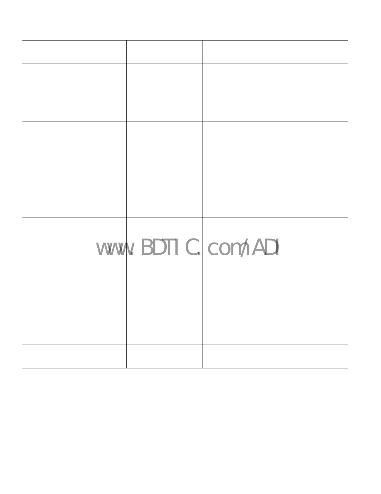
(VDD = 5 V 10%, GND = 0 V. All specifications
www.BDTIC.com/ADI
ADG781/ADG782/ADG783–SPECIFICATIONS
–40C to +85C unless otherwise noted.)
B Version
–40C to
Parameter +25C +85C Unit Test Conditions/Comments
ANALOG SWITCH
Analog Signal Range 0 V to V
On Resistance (R
) 2.5 Ω typ VS = 0 V to VDD, IS = –10 mA;
ON
DD
V
4 4.5 Ω max Test Circuit 1
On-Resistance Match Between 0.05 Ω typ V
Channels (∆R
On-Resistance Flatness (R
) 0.4 Ω max
ON
FLAT(ON)
) 0.5 Ω typ VS = 0 V to VDD, IS = –10 mA
= 0 V to VDD, IS = –10 mA
S
1.0 Ω max
LEAKAGE CURRENTS V
Source OFF Leakage I
(OFF) ± 0.01 nA typ VS = 4.5 V/1 V, VD = 1 V/4.5 V;
S
= 5.5 V;
DD
± 0.1 ± 0.2 nA max Test Circuit 2
Drain OFF Leakage I
(OFF) ± 0.01 nA typ VS = 4.5 V/1 V, VD = 1 V/4.5 V;
D
± 0.1 ± 0.2 nA max Test Circuit 2
Channel ON Leakage I
, IS (ON) ± 0.01 nA typ VS = VD = 1 V, or 4.5 V;
D
± 0.1 ± 0.2 nA max Test Circuit 3
DIGITAL INPUTS
Input High Voltage, V
Input Low Voltage, V
INL
INH
2.4 V min
0.8 V max
Input Current
I
INL
or I
INH
0.005 µA typ VIN = V
INL
or V
INH
± 0.1 µA max
DYNAMIC CHARACTERISTICS
t
ON
t
OFF
Break-Before-Make Time Delay, t
(ADG783 Only) 1 ns min V
Charge Injection 3 pC typ V
2
11 ns typ RL = 300 Ω, CL = 35 pF,
16 ns max V
= 3 V; Test Circuit 4
S
6 ns typ RL = 300 Ω, CL = 35 pF,
10 ns max V
D
6 ns typ RL = 300 Ω, CL = 35 pF,
= 3 V; Test Circuit 4
S
= VS2 = 3 V; Test Circuit 5
S1
= 2 V; RS = 0 Ω, CL = 1 nF;
S
Test Circuit 6
Off Isolation –58 dB typ R
–78 dB typ R
= 50 Ω, CL = 5 pF, f = 10 MHz
L
= 50 Ω, CL = 5 pF, f = 1 MHz;
L
Test Circuit 7
Channel-to-Channel Crosstalk –90 dB typ R
= 50 Ω, CL = 5 pF, f = 10 MHz;
L
Test Circuit 8
Bandwidth –3 dB 200 MHz typ R
C
(OFF) 10 pF typ f = 1 MHz
S
C
(OFF) 10 pF typ f = 1 MHz
D
= 50 Ω, CL = 5 pF; Test Circuit 9
L
CD, CS (ON) 22 pF typ f = 1 MHz
POWER REQUIREMENTS V
I
DD
0.001 µA typ Digital Inputs = 0 V or 5.5 V
= 5.5 V
DD
1.0 µA max
NOTES
1
Temperature ranges are as follows: B Version: –40°C to +85°C.
2
Guaranteed by design, not subject to production test.
Specifications subject to change without notice.
–2–
REV. A

ADG781/ADG782/ADG783
www.BDTIC.com/ADI
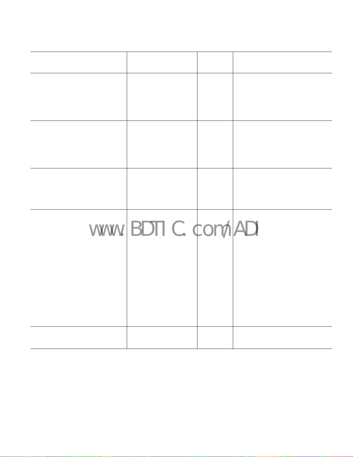
SPECIFICATIONS
Parameter +25C +85C Unit Test Conditions/Comments
ANALOG SWITCH
Analog Signal Range 0 V to V
On Resistance (R
On-Resistance Match Between 0.1 Ω typ V
Channels (∆R
On-Resistance Flatness (R
LEAKAGE CURRENTS V
Source OFF Leakage I
Drain OFF Leakage I
Channel ON Leakage I
DIGITAL INPUTS
Input High Voltage, V
Input Low Voltage, V
Input Current
I
or I
INL
INH
DYNAMIC CHARACTERISTICS
t
ON
t
OFF
Break-Before-Make Time Delay, t
(ADG783 Only) 1 ns min V
Charge Injection 3 pC typ V
Off Isolation –58 dB typ R
Channel-to-Channel Crosstalk –90 dB typ R
Bandwidth –3 dB 200 MHz typ R
C
(OFF) 10 pF typ f = 1 MHz
S
C
(OFF) 10 pF typ f = 1 MHz
D
CD, CS (ON) 22 pF typ f = 1 MHz
POWER REQUIREMENTS V
I
DD
NOTES
1
Temperature ranges are as follows: B Version: –40°C to +85°C.
2
Guaranteed by design, not subject to production test.
Specifications subject to change without notice.
) 5 5.5 Ω typ VS = 0 V to VDD, IS = –10 mA;
ON
) 0.5 Ω max
ON
S
(OFF) ± 0.01 nA typ VS = 3 V/1 V, VD = 1 V/3 V;
D
D
INH
INL
1
(VDD = 3 V 10%, GND = 0 V. All specifications –40C to +85C unless otherwise noted.)
B Version
–40C to
V
DD
10 Ω max Test Circuit 1
= 0 V to VDD, IS = –10 mA
S
FLAT(ON)
(OFF) ±0.01 nA typ VS = 3 V/1 V, VD = 1 V/3 V;
, IS (ON) ±0.01 nA typ VS = VD = 1 V, or 3 V;
) 2.5 Ω typ VS = 0 V to VDD, IS = –10 mA
= 3.3 V;
DD
± 0.1 ±0.2 nA max Test Circuit 2
± 0.1 ±0.2 nA max Test Circuit 2
± 0.1 ±0.2 nA max Test Circuit 3
2.0 V min
0.8 V max
0.005 µA typ VIN = V
INL
or V
INH
± 0.1 µA max
2
13 ns typ RL = 300 Ω, CL = 35 pF,
20 ns max V
= 2 V; Test Circuit 4
S
7 ns typ RL = 300 Ω, CL = 35 pF,
12 ns max V
D
7 ns typ RL = 300 Ω, CL = 35 pF,
= 2 V; Test Circuit 4
S
= VS2 = 2 V; Test Circuit 5
S1
= 1.5 V; RS = 0 Ω, CL = 1 nF;
S
Test Circuit 6
= 50 Ω, CL = 5 pF, f = 10 MHz
–78 dB typ R
L
= 50 Ω, CL = 5 pF, f = 1 MHz;
L
Test Circuit 7
= 50 Ω, CL = 5 pF, f = 10 MHz;
L
Test Circuit 8
= 50 Ω, CL = 5 pF; Test Circuit 9
L
= 3.3 V
DD
0.001 µA typ Digital Inputs = 0 V or 3.3 V
1.0 µA max
REV. A
–3–
 Loading...