


Low Voltage, 400 MHz, Quad 2:1
www.BDTIC.com/ADI
FEATURES
Bandwidth: >400 MHz
Low insertion loss and on resistance: 2.2 Ω typical
On resistance flatness: 0.3 Ω typical
Single 3 V/5 V supply operation
Very low distortion: <0.3%
Low quiescent supply current:
Fast switching times
= 6 ns
t
ON
t
= 3 ns
OFF
TTL-/CMOS-compatible
Pb-free packages
16-lead QSSOP
16-lead 3 mm × 3 mm body LFCSP
GENERAL DESCRIPTION
The ADG774A is a monolithic CMOS device comprising four
2:1 multiplexer/demultiplexers with high impedance outputs.
The CMOS process provides low power dissipation yet offers
high switching speed and low on resistance. The on resistance
variation is typically less than 0.5 Ω over the input signal range.
The bandwidth of the ADG774A is typically 400 MHz and this,
upled with low distortion (typically 0.3%), makes the part
co
suitable for switching of high speed data signals.
1 nA typical
Mux with 3 ns Switching Time
ADG774A
FUNCTIONAL BLOCK DIAGRAM
S1A
S1B
S2A
S2B
S3A
S3B
S4A
S4B
These switches conduct equally well in both directions when
o
n. In the off condition, signal levels up to the supplies are
blocked. The ADG774A switches exhibit break-before-make
switching action.
PRODUCT HIGHLIGHTS
1. Wide bandwidth data rates of >400 MHz.
2. Ultralow power dissipation.
ADG774A
1 OF 2
DECODER
IN
EN
Figure 1.
D1
D2
D3
D4
2373-001
The on resistance profile is very flat over the full analog input
nge ensuring excellent linearity and low distortion. CMOS
ra
construction ensures ultralow power dissipation.
The ADG774A operates from a single 3.3 V/5 V supply and is
TL logic-compatible. The control logic for each switch is
T
shown in the truth table (see Tab le 5 ).
Rev. B
Information furnished by Analog Devices is believed to be accurate and reliable. However, no
responsibility is assumed by Anal og Devices for its use, nor for any infringements of patents or ot her
rights of third parties that may result from its use. Specifications subject to change without notice. No
license is granted by implication or otherwise under any patent or patent rights of Analog Devices.
Trademarks and registered trademarks are the property of their respective owners.
3. Low leakage over temperature.
4. Break-before-make switching prevents channel shorting
hen the switches are configured as a multiplexer.
w
5. Crosstalk is typically −70 dB @ 10 MHz.
6. Off isolation is typically −65 dB @ 10 MHz.
7. Available in compact 3 mm × 3 mm LFCSP.
One Technology Way, P.O. Box 9106, Norwood, MA 02062-9106, U.S.A.
Tel: 781.329.4700 www.analog.com
Fax: 781.461.3113 ©2006 Analog Devices, Inc. All rights reserved.

ADG774A
www.BDTIC.com/ADI
TABLE OF CONTENTS
Features.............................................................................................. 1
ESD Caution...................................................................................5
Functional Block Diagram .............................................................. 1
General Description ......................................................................... 1
Product Highlights ........................................................................... 1
Revision History ............................................................................... 2
Specifications..................................................................................... 3
Single Supply................................................................................. 3
Absolute Maximum Ratings............................................................ 5
REVISION HISTORY
8/06—Rev. A to Rev. B
Updated Format..................................................................Universal
Added LFCSP Model..........................................................Universal
Added Lead-Free Models ..................................................Universal
Changes to Table 3.............................................................................5
Updated Outline Dimensions....................................................... 13
Changes to Ordering Guide.......................................................... 13
Pin Configurations and Function Descriptions............................6
Typical Performance Characteristics..............................................7
Test Circuits........................................................................................9
Terminology.................................................................................... 11
Application Circuits ....................................................................... 12
Outline Dimensions....................................................................... 13
Ordering Guide .......................................................................... 13
4/03—Rev. 0 to Rev. A
C
hanges to TPCs 9–11......................................................................5
Updated Outline Dimensions..........................................................8
7/01—Revision 0: Initial Version
Rev. B | Page 2 of 16

ADG774A
www.BDTIC.com/ADI
SPECIFICATIONS
SINGLE SUPPLY
VDD = 5 V ± 10%, GND = 0 V, all specifications T
MIN
to T
, unless otherwise noted.
MAX
Table 1.
B Version
Parameter 25°C T
MIN
to T
Unit Test Conditions/Comments
MAX
ANALOG SWITCH
Analog Signal Range 0 to 2.5 V
On Resistance, RON 2.2 Ω typ VD = 0 V to 1 V, IS = −10 mA
3.5 4 Ω max
On Resistance Match Between Channels, ∆RON 0.15 Ω typ VD = 0 V to 1 V, IS = −10 mA
0.5 Ω max
On Resistance Flatness, R
0.3 Ω typ VD = 0 V to 1 V, IS = −10 mA
FLAT(ON)
0.6 Ω max
LEAKAGE CURRENTS
Source Off Leakage, IS (OFF) ±0.001 nA typ VD = 3 V/1 V, VS = 1 V/3 V, see Figure 17
±0.1 ±0.25 nA max
Drain Off Leakage, ID (OFF) ±0.001 nA typ VD = 3 V/1 V, VS = 1 V/3 V, see Figure 17
±0.1 ±0.25 nA max
Channel On Leakage, ID, IS (ON) ±0.001 nA typ VD = VS = 3 V/1 V, see Figure 18
±0.1 ±0.25 nA max
DIGITAL INPUTS
Input High Voltage, V
Input Low Voltage, V
2.4 V min
INH
0.8 V max
INL
Input Current
I
or I
INL
0.001 μA typ VIN = V
INH
±0.1 μA max
Digital Input Capacitance, CIN 3 pF typ
DYNAMIC CHARACTERISTICS
tON, tON (EN)
2
6 ns typ C
12 ns max
t
, t
(EN)
OFF
OFF
3 ns typ C
6 ns max
Break-Before-Make Time Delay, tD 3 ns typ CL = 35 pF, RL = 50 Ω, VS1 = VS2 = 2 V, see Figure 23
1 ns min
Off Isolation −65 dB typ f = 10 MHz, RL = 50 Ω, see Figure 20
Channel-to-Channel Crosstalk −70 dB typ f = 10 MHz, RL = 50 Ω, see Figure 21
Bandwidth −3 dB 400 MHz typ RL = 50 Ω, see Figure 19
Distortion 0.3 % typ RL = 100 Ω
Charge Injection 6 pC typ CL = 1 nF, see Figure 24, VS = 0 V
CS (OFF) 5 pF typ
CD (OFF) 7.5 pF typ
CD, CS (ON) 12 pF typ
POWER REQUIREMENTS VDD = 5.5 V
Digital inputs = 0 V or VDD
IDD 1 μA max
0.001 μA typ
1
Temperature range for B version is −40°C to +85°C.
2
Guaranteed by design, not subject to production test.
1
or V
INH
INL
= 35 pF, RL = 50 Ω, VS = 2 V, see Figure 22
L
= 35 pF, RL = 50 Ω, VS = 2 V, see Figure 22
L
Rev. B | Page 3 of 16

ADG774A
www.BDTIC.com/ADI
VDD = 3 V ± 10%, GND = 0 V, all specifications T
MIN
to T
, unless otherwise noted.
MAX
1
Table 2.
B Version
Parameter 25°C T
MIN
to T
Unit Test Conditions/Comments
MAX
ANALOG SWITCH
Analog Signal Range 0 to 1.5 V
On Resistance, RON 4 Ω typ VD = 0 V to 1 V; IS = −10 mA
6 7 Ω max
On Resistance Match Between Channels, ∆RON
0.15 Ω typ VD = 0 V to 1 V, IS = −10 mA
0.5 Ω max
On Resistance Flatness, R
1.5 Ω typ VD = 0 V to 1 V, IS = −10 mA
FLAT(ON)
3 Ω max
LEAKAGE CURRENTS
Source Off Leakage, IS (OFF) ±0.001 nA typ VD = 2 V/1 V, VS = 1 V/2 V, see Figure 17
±0.1 ±0.25 nA max
Drain Off Leakage, ID (OFF) ±0.001 nA typ VD = 2 V/1 V, VS = 1 V/2 V, see Figure 17
±0.1 ±0.25 nA max
Channel On Leakage, ID, IS(ON) ±0.001 nA typ VD = VS = 2 V/1 V, see Figure 18
±0.1 ±0.25 nA max
DIGITAL INPUTS
Input High Voltage, V
Input Low Voltage, V
2.0 V min
INH
0.4 V max
INL
Input Current
I
or I
INL
0.001 μA typ VIN = V
INH
INL
or V
INH
±0.1 μA max
Digital Input Capacitance, CIN 3 pF typ
DYNAMIC CHARACTERISTICS
tON, tON (EN)
2
7 ns typ C
= 35 pF, RL = 50 Ω, VS = 1.5 V, see Figure 22
L
14 ns max
t
, t
(EN)
OFF
OFF
4 ns typ C
= 35 pF, RL = 50 Ω, VS = 1.5 V, see Figure 22
L
8 ns max
Break-Before-Make Time Delay, tD 3 ns typ CL = 35 pF, RL = 50 Ω, VS1 = VS2 = 1.5 V, see Figure 23
1 ns min
Off Isolation −65 dB typ f = 10 MHz, RL = 50 Ω
Channel-to-Channel Crosstalk −70 dB typ f = 10 MHz, RL = 50 Ω, see Figure 21
Bandwidth −3 dB 400 MHz typ RL = 50 Ω, see Figure 19
Distortion 1.5 % typ RL = 100 Ω
Charge Injection 4 pC typ CL = 1 nF, see Figure 24, VS = 0 V
CS (OFF) 5 pF typ
CD (OFF) 7.5 pF typ
CD, CS (ON) 12 pF typ
POWER REQUIREMENTS VDD = 3.3 V
Digital inputs = 0 V or VDD
IDD 1 μA max
0.001 μA typ
1
Temperature range for B version is −40°C to +85°C.
2
Guaranteed by design, not subject to production test.
Rev. B | Page 4 of 16

ADG774A
www.BDTIC.com/ADI
ABSOLUTE MAXIMUM RATINGS
TA = 25°C, unless otherwise noted.
Table 3.
Parameters Rating
VDD to GND −0.3 V to +6 V
Analog, Digital Inputs
Continuous Current, S or D 100 mA
Peak Current, S or D
Operating Temperature Range
Industrial (B Version) −40°C to +85°C
Storage Temperature Range −65°C to +150°C
Junction Temperature 150°C
Thermal Impedance, θJA
16-Lead QSSOP 105.44°C/W
16-Lead LFCSP(3 mm × 3 mm) 48.7°C/W
Lead Temperature Soldering
Vapor Phase (60 sec) 215°C
Infrared (15 sec) 220°C
Reflow Soldering (Pb-free)
Peak Temperature 260°C (+0°C/–5°C)
Time at Peak Temperature 10 sec to 40 sec
1
Overvoltages at IN, S, or D are clamped by internal diodes. Current should be
limited to the maximum ratings given.
2
Measured with the device soldered on a four-layer board.
1
−0.3 V to VDD + 0.3 V or 30 mA,
whichever occurs first
300 mA (pulsed at 1 ms,
10% duty c
ycle max)
2
2
Stresses above those listed under Absolute Maximum Ratings
ma
y cause permanent damage to the device. This is a stress
rating only; functional operation of the device at these or any
other conditions above those listed in the operational sections
of this specification is not implied. Exposure to absolute
maximum rating conditions for extended periods may affect
device reliability. Only one absolute maximum rating may be
applied at any one time.
ESD CAUTION
Rev. B | Page 5 of 16

ADG774A
www.BDTIC.com/ADI
PIN CONFIGURATIONS AND FUNCTION DESCRIPTIONS
DD
IN
EN
S1A
V
13
14
15
1S1B
2D1
3S2A
4S2B
16
PIN 1
INDICATOR
ADG774A
TOP VIEW
(Not to Scale)
7
5
6
D2
D3
GND
8
S3B
12 S4A
11 S4B
10 D4
9S3A
02373-028
1
IN
2
S1A
3
S1B
D1
S2A
S2B
D2
GND
ADG774A
4
TOP VIEW
5
(Not to Scale)
6
7
8
Figure 2. QSOP Pin Configur
V
16
DD
EN
15
14
S4A
13
S4B
12
D4
11
S3A
10
S3B
9
D3
2373-002
NOTES
1. THE EXPOSED PAD SHOULD
BE TIED TO GND.
ation Figure 3. LFCSP Pin Configuration
Table 4. Pin Function Descriptions
Pin No.
QSOP LFCSP
Mnemonic Function
1 15 IN Logic Control Input.
2 16 S1A Source Terminal 1A. May be an input or output.
3 1 S1B Source Terminal 1B May be an input or output.
4 2 D1 Drain Terminal D1. May be an input or output.
5 3 S2A Source Terminal 2A. May be an input or output.
6 4 S2B Source Terminal 2B. May be an input or output.
7 5 D2 Drain Terminal D2. May be an input or output.
8 6 GND Ground (0 V) Reference.
9 7 D3 Drain Terminal D3. May be an input or output.
10 8 S3B Source Terminal 3B. May be an input or output.
11 9 S3A Source Terminal 3A. May be an input or output.
12 10 D4 Drain Terminal D4. May be an input or output.
13 11 S4B Source Terminal 4B. May be an input or output.
14 12 S4A Source Terminal 4A. May be an input or output.
15 13
EN
Logic Control Input. When high, all switches are disabled.
16 14 VDD Most Positive Power Supply Potential.
Table 5. Truth Table
EN
IN D1 D2 D3 D4 Function
1 X Hi-Z Hi-Z Hi-Z Hi-Z DISABLE
0 0 S1A S2A S3A S4A IN = 0
0 1 S1B S2B S3B S4B IN = 1
Rev. B | Page 6 of 16

ADG774A
www.BDTIC.com/ADI
TYPICAL PERFORMANCE CHARACTERISTICS
20
= 25°C
T
A
20
= 3V
V
DD
16
VDD = 5.0V
12
(Ω)
ON
R
8
4
0
05
1234
Figure 4. On Resistance as a Function of Drain ( V
Volta ge for V
20
TA = 25°C
16
12
(Ω)
ON
R
8
4
0
03
VDD = 2.7V
0.51.01.52.02.5
Figure 5. On Resistance as a Function of Drain ( V
Voltage fo r V
VDD = 3.0V
V
= 4.5V
DD
V
(V)
S/VD
= 5 V ± 10%
DD
(V)
V
S/VD
= 3 V ± 10%
DD
VDD = 3.3V
= 5.5V
V
DD
) or Source (VS)
D
) or Source (VS)
D
02373-003
.0
02373-004
15
(Ω)
10
ON
R
5
0
03
+25°C
0.51.01.52.02.5
Figure 7. On Resistance as a Function of Drain ( V
for Different Temperatures with 3 V Single Supplies
0.025
VDD = 5.0V
V
= 0V
SS
0.020
TEMP = 25°C
V
= VDD – V
D
0.015
0.010
0.005
0
–0.005
CURRENT (nA)
–0.010
–0.015
–0.020
–0.025
04
V
S
I
S
ID (OFF)
(OFF)
Figure 8. Leakage Current as a Function of Drain (V
+85°C
–40°C
V
(V)
S/VD
) or Source (VS) Voltage
D
S
, ID (ON)
I
S
123
V
(V)
S/VD
) or Source (VS)
Volta ge for V
DD
= 5 V
D
.0
02373-006
02373-007
20
VDD = 5V
15
(Ω)
10
ON
R
5
0
05
+25°C
1234
Figure 6. On Resistance as a Function of Drain ( V
V
S/VD
+85°C
(V)
–40°C
) or Source (VS)
D
02373-005
Voltage for Different Temperatures with 5 V Single Supplies
Rev. B | Page 7 of 16
0.025
VDD = 3.0V
V
0.020
0.015
0.010
0.005
–0.005
CURRENT (nA)
–0.010
–0.015
–0.020
–0.025
Figure 9. Leakage Current as a Function of Drain (V
= 0V
SS
TEMP = 25° C
V
= VDD – V
D
ID (OFF)
0
IS (OFF)
03
V
S
S
IS, ID (ON)
0.5 1.0 1.5 2.0 2.5
V
(V)
S/VD
) or Source (VS)
Volta ge for V
DD
= 3 V
D
.0
02373-008

ADG774A
www.BDTIC.com/ADI
0.05
VDD = 5.0V
V
= 0V
0.04
SS
TEMP = 25° C
V
= 3V/1V
0.03
D
V
= 1V/3V
S
0.02
0.01
–0.01
CURRENT (nA)
–0.02
–0.03
–0.04
–0.05
ID (OFF)
0
I
(OFF)
S
585
15 25 35 45 55 65 75
IS, ID (ON)
TEMPERATURE (°C)
Figure 10. Leakage Current as a Function of Temperature, V
0.05
VDD = 3.0V
= 0V
V
0.04
SS
TEMP = 25° C
= 2V/1V
V
D
0.03
= 1V/2V
V
S
0.02
0.01
0
–0.01
CURRENT (nA)
–0.02
–0.03
–0.04
–0.05
58
ID (OFF)
15 25 35 45 55 65 75
TEMPERATURE (°C)
IS (OFF)
Figure 11. Leakage Current as a Function of Temperature, V
0
IS, ID (ON)
0
–20
–40
–60
ATTENUATIO N (dB)
–80
–100
0.01 1000
02373-009
= 5 V
DD
0
–5
–10
ON RESPONSE (dB)
5
02373-010
= 3 V
DD
–15
0.01 1000
0
0.1 1 10 100
Figure 13. Cross talk vs. Frequency
0.1 1 10 100
FREQUENCY (MHz)
FREQUENCY (MHz)
Figure 14. Bandwidth
02373-012
02373-013
–20
–40
–60
ATTENUATIO N (dB)
–80
–100
0.01 1000
0.1 1 10 100
FREQUENCY (M Hz)
Figure 12. Off Isolation vs. Frequency
02373-011
Rev. B | Page 8 of 16
–1
–2
–3
(pC)
INJ
–4
Q
–5
–6
–7
02
0.5 1.0 1.5 2.0
VDD = 3V
= 5V
V
DD
VOLTAGE (V)
.5
02373-014
Figure 15. Charge Injection vs. Source Voltage

ADG774A
V
V
V
V
V
V
V
www.BDTIC.com/ADI
TEST CIRCUITS
DD
0.1µF
I
DS
V1
SD
S
RON = V1/I
Figure 16. On Resistance
DS
02373-019
IN
IN
ADG774A
EN
GND
DD
0.1µF
S1A
D1
Figure 19. Bandwidth
NETWORK
ANALYZER
50Ω
V
S
V
50Ω
OUT
2373-024
IS (OFF) ID (OFF)
SD
A
V
S
Figure 17. Off Leakage
NC
SD
NC = NO CONNECT
ID (ON)
A
V
ADG774A
A
V
D
02373-020
IN
IN
EN
S1A
50Ω
D1
GND
NETWORK
ANALYZER
50Ω
V
S
V
50Ω
OUT
02373-025
Figure 20. Off Isolation
DD
0.1µF
NETWORK
ADG774A
S1A
S2A
D
02373-021
IN
ANALYZER
50Ω
V
S
V
OUT
R
L
50Ω
Figure 18. On Leakage
Rev. B | Page 9 of 16
GND
D2
D1
50Ω
02373-026
IN
EN
Figure 21. Channel-to-Channel Crosstalk

ADG774A
V
V
V
V
www.BDTIC.com/ADI
5
0.1µF
3V
V
V
DD
V
C
L
35pF
OUT
SD
S
IN
GND
EN
R
L
100Ω
IN
V
OUT
50% 50%
90% 90%
t
ON
t
OFF
02373-022
Figure 22. Switching Times
5
0.1µF
V
DD
S1A
V
S1B
S
V
EN
S
DECODER
GND
D1
R
100Ω
V
OUT
C
L
L
35pF
3V
V
IN
0V
V
OUT
V
S
50% 50%
80% 80%
t
D
t
D
2373-023
Figure 23. Break-Before-Make Time Delay
5
V
DD
R
S
V
S
S1A
S1B
S2A
S2B
S3A
S3B
S4A
S4B
ADG774A
1 OF 2
DECODER
EN
D1 V
D2 V
D3 V
D4 V
OUT
OUT
OUT
OUT
C
L
1nF
C
L
1nF
C
L
1nF
C
L
1nF
IN
3V
V
IN
V
OUT
Q
= CL × ΔV
INJ
OUT
ΔV
OUT
02373-027
Figure 24. Charge Injection
Rev. B | Page 10 of 16

ADG774A
www.BDTIC.com/ADI
TERMINOLOGY
VDD
Most positive power supply potential.
V
(VS)
D
Analog voltage on the D and S terminals.
GND
Ground (0 V) reference.
S
Source terminal. May be an input or output.
D
Drain terminal. May be an input or output.
IN
Logic control input.
EN
Logic control input.
R
ON
Ohmic resistance between D and S.
∆R
ON
On resistance match between any two channels, that is,
max − RON min.
R
ON
FLAT(ON)
R
Flatness is defined as the difference between the maximum and
inimum value of on resistance as measured over the specified
m
analog signal range.
I
(OFF)
S
Source leakage current with the switch off.
I
(OFF)
D
Drain leakage current with the switch off.
C
(OFF)
S
Off switch source capacitance.
(OFF)
C
D
Off switch drain capacitance.
C
, CS (ON)
D
On switch capacitance.
t
ON
Delay between applying the digital control input and the output
tching on. See Figure 22.
swi
t
OFF
Delay between applying the digital control input and the output
swi
tching off.
t
D
Off time or on time measured between the 80% points of both
witches when switching from one address state to another. See
s
Figure 23.
Crosstalk
A measure of unwanted signal that is coupled through from one
ch
annel to another because of parasitic capacitance.
Off Isolation
A measure of unwanted signal coupling through an off switch.
Bandwidth
Frequency response of the switch in the on state measured at
wn.
3 dB do
I
, IS (ON)
D
Channel leakage current with the switch on.
Rev. B | Page 11 of 16
Distortion
R
FLAT(ON)/RL

ADG774A
www.BDTIC.com/ADI
APPLICATION CIRCUITS
10 BASE Tx+
10 BASE Tx–
Tx1
ADG774A
100 BASE Tx+
100 BASE Tx–
10 BASE Tx+
10 BASE Tx–
100 BASE Tx+
100 BASE Tx–
10 BASE Tx
100 BASE Tx
Tx2
Rx1
Rx2
TRANSFORMER
RJ45
02373-015
Figure 25. Full Duplex Transceiver
Tx1
120
Rx1
Ω
02373-016
100
Ω
02373-017
02373-018
Figure 26. Loop Back Figure 27. Line Termination Figure 28. Line Clamp
Rev. B | Page 12 of 16
ADG774A
R
R
www.BDTIC.com/ADI
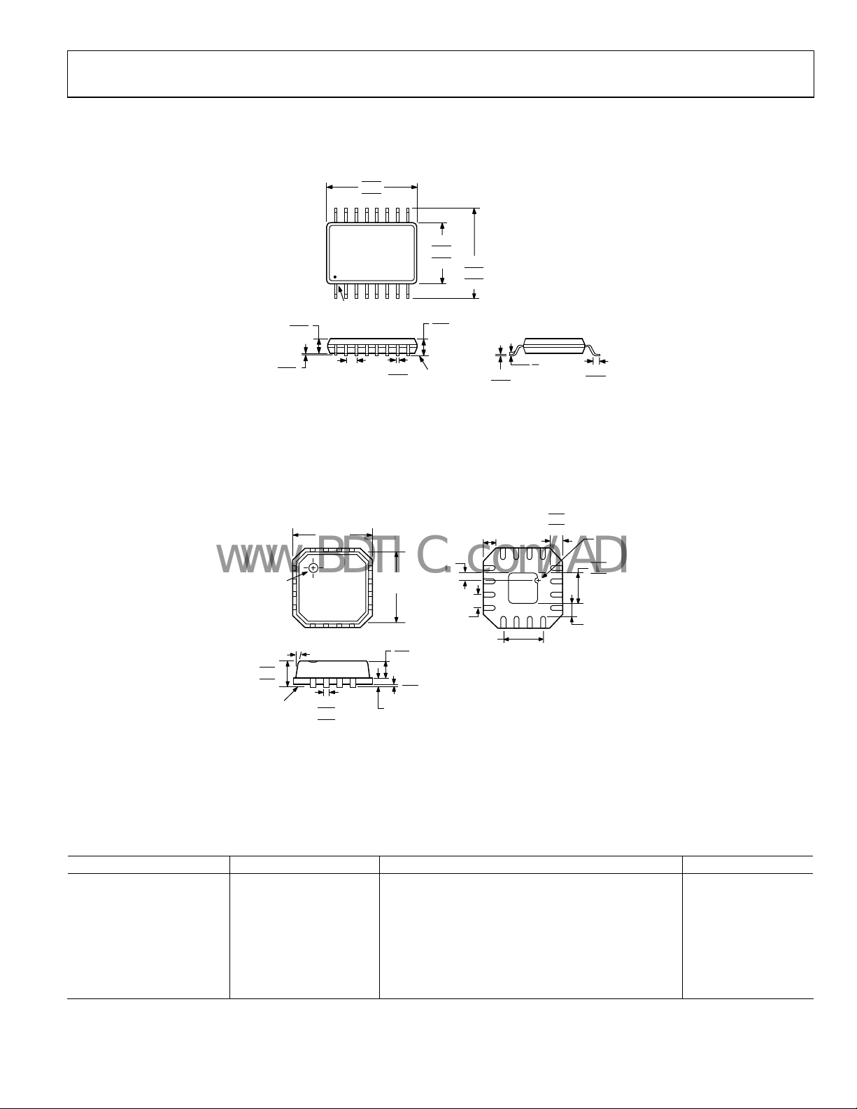
OUTLINE DIMENSIONS
0.197
0.193
0.189
0.012
0.008
9
8
0.158
0.154
0.150
0.069
0.053
SEATING
PLANE
0.244
0.236
0.228
0.010
0.006
8°
0°
0.050
0.016
0.065
0.049
0.010
0.004
COPLANARITY
0.004
16
1
PIN 1
0.025
BSC
COMPLIANT TO JEDEC STANDARDS MO-137-AB
Figure 29. 16-Lead Shrink Small Outline Package [QSOP]
Q-16)
(R
Dimensions shown in inches
0.50
0.40
PIN 1
INDICATO
0.90
0.85
0.80
SEATING
PLANE
12° MAX
3.00
BSC SQ
TOP
VIEW
0.30
0.23
0.18
*
COMPLIANT
EXCEPT FOR EXPOSED PAD DIMENSION.
2.75
BSC SQ
0.80 MAX
0.65 TYP
0.05 MAX
0.02 NOM
0.20 REF
TO
JEDEC STANDARDS MO-220-VEED-2
0.45
0.50
BSC
1.50 REF
0.60 MAX
13
12
(BOTTOM VIEW)
9
8
Figure 30. 16-Lead Lead Frame Chip Scale Package [LFCSP_VQ]
(CP-16-3)
Dim
ensions shown in millimeters
EXPOSED
PAD
0.30
16
1
4
5
N
I
P
D
N
I
*
1.65
1.50 SQ
1.35
0.25 MIN
1
O
T
C
I
A
ORDERING GUIDE
Model Temperature Range Package Description Package Option
ADG774ABRQ
ADG774ABRQ-REEL
ADG774ABRQ-REEL7
ADG774ABRQZ
1
ADG774ABRQZ-REEL
ADG774ABRQZ-REEL7
ADG774ABCPZ-REEL
1
Z = Pb-free part.
1
1
−40°C to +85°C
−40°C to +85°C
−40°C to +85°C
−40°C to +85°C
−40°C to +85°C
−40°C to +85°C
−40°C to +85°C
16-Lead Shrink Small Outline Package [QSOP] RQ-16
16-Lead Shrink Small Outline Package [QSOP] RQ-16
16-Lead Shrink Small Outline Package [QSOP] RQ-16
16-Lead Shrink Small Outline Package [QSOP] RQ-16
16-Lead Shrink Small Outline Package [QSOP] RQ-16
16-Lead Shrink Small Outline Package [QSOP] RQ-16
16-Lead Lead Frame Chip Scale Package [LFCSP_VQ] CP-16-3
Rev. B | Page 13 of 16

ADG774A
www.BDTIC.com/ADI
NOTES
Rev. B | Page 14 of 16

ADG774A
www.BDTIC.com/ADI
NOTES
Rev. B | Page 15 of 16

ADG774A
www.BDTIC.com/ADI
NOTES
©2006 Analog Devices, Inc. All rights reserved. Trademarks and
registered trademarks are the property of their respective owners.
C02373-0-8/06(B)
Rev. B | Page 16 of 16
 Loading...