Analog Devices ADG741 2 Datasheet

CMOS Low Voltage
IN
S
D
ADG741
IN
S
D
ADG742
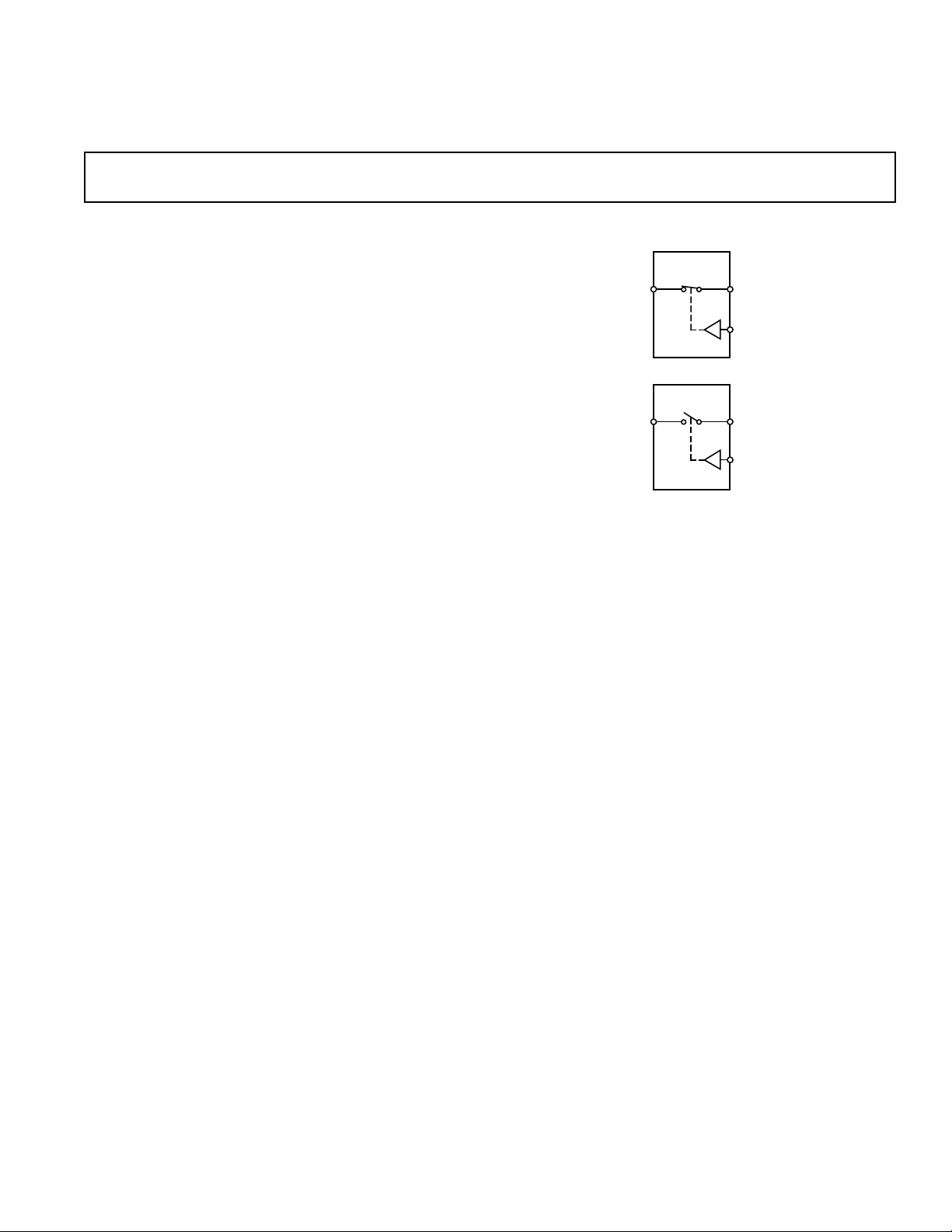
SWITCHES SHOWN FOR
A LOGIC "1" INPUT
a
FEATURES
1.8 V to 5.5 V Single Supply
2 ⍀ (Typ) On Resistance
Low On-Resistance Flatness
–3 dB Bandwidth >200 MHz
Rail-to-Rail Operation
6-Lead SC70
Fast Switching Times
18 ns
t
ON
12 ns
t
OFF
Typical Power Consumption (<0.01 W)
TTL/CMOS Compatible
APPLICATIONS
Battery Powered Systems
Communication Systems
Sample Hold Systems
Audio Signal Routing
Video Switching
Mechanical Reed Relay Replacement
2 ⍀ SPST Switches in SC70 Packages
ADG741/ADG742
FUNCTIONAL BLOCK DIAGRAMS
GENERAL DESCRIPTION
The ADG741/ADG742 are monolithic CMOS SPST switches.
These switches are designed on an advanced submicron process
that provides low power dissipation yet high switching speed,
low on resistance, low leakage currents and –3 dB bandwidths of
greater than 200 MHz can be achieved.
The ADG741/ADG742 can operate from a single 1.8 V to 5.5 V
supply, making it ideal for use in battery-powered instruments
and with Analog Devices’ new generation of DACs and ADCs.
As can be seen from the Functional Block Diagrams, with a
logic input of “1” the switch of the ADG741 is closed, while
that of the ADG742 is open. Each switch conducts equally well
in both directions when ON.
The ADG741/ADG742 are available in 6-lead SC70 package.
PRODUCT HIGHLIGHTS
1. 1.8 V to 5.5 V Single Supply Operation. The ADG741/
ADG742 offer high performance, including low on resistance
and fast switching times and is fully specified and guaranteed
with 3 V and 5 V supply rails.
2. Very Low R
operation, R
3. On-Resistance Flatness R
(3 Ω max at 5 V, 5 Ω max at 3 V). At 1.8 V
ON
is typically 40 Ω over the temperature range.
ON
FLAT(ON)
(1 Ω max).
4. –3 dB Bandwidth >200 MHz.
5. Low Power Dissipation. CMOS construction ensures low
power dissipation.
6. Fast t
ON/tOFF.
7. Tiny 6-Lead SC70 package.
REV. 0
Information furnished by Analog Devices is believed to be accurate and
reliable. However, no responsibility is assumed by Analog Devices for its
use, nor for any infringements of patents or other rights of third parties
which may result from its use. No license is granted by implication or
otherwise under any patent or patent rights of Analog Devices.
One Technology Way, P.O. Box 9106, Norwood, MA 02062-9106, U.S.A.
Tel: 781/329-4700 World Wide Web Site: http://www.analog.com
Fax: 781/326-8703 © Analog Devices, Inc., 2000

(VDD = 5 V ⴞ 10%, GND = 0 V. All specifications –40ⴗC to +85ⴗC
1
ADG741/ADG742–SPECIFICATIONS
unless otherwise noted.)
B Version
Parameter 25ⴗC –40ⴗC to +85ⴗC Unit Test Conditions/Comments
ANALOG SWITCH
Analog Signal Range 0 V to V
On Resistance (R
)2 Ω typ VS = 0 V to VDD, IS = –10 mA;
ON
DD
V
34 Ω max Test Circuit 1
On-Resistance Flatness (R
FLAT(ON)
) 0.5 Ω typ VS = 0 V to VDD, IS = –10 mA
1.0 Ω max
LEAKAGE CURRENTS
Source OFF Leakage I
2
(OFF) ±0.01 nA typ VS = 4.5 V/1 V, VD = 1 V/4.5 V;
S
V
= 5.5 V
DD
±0.25 ±0.35 nA max Test Circuit 2
Drain OFF Leakage I
(OFF) ±0.01 nA typ VS = 4.5 V/1 V, VD = 1 V/4.5 V;
D
±0.25 ±0.35 nA max Test Circuit 2
Channel ON Leakage I
, IS (ON) ±0.01 nA typ VS = VD = 1 V, or 4.5 V;
D
±0.25 ±0.35 nA max Test Circuit 3
DIGITAL INPUTS
Input High Voltage, V
Input Low Voltage, V
INL
INH
2.4 V min
0.8 V max
Input Current
I
INL
or I
INH
0.005 µA typ VIN = V
INL
or V
INH
±0.1 µA max
DYNAMIC CHARACTERISTICS
t
ON
t
OFF
Charge Injection 5 pC typ V
2
12 ns typ RL = 300 Ω, CL = 35 pF
18 ns max V
= 3 V; Test Circuit 4
S
8 ns typ RL = 300 Ω, CL = 35 pF
12 ns max V
= 3 V; Test Circuit 4
S
= 2 V, RS = 0 Ω, CL = 1 nF;
S
Test Circuit 5
Off Isolation –55 dB typ R
–75 dB typ R
= 50 Ω, CL = 5 pF, f = 10 MHz
L
= 50 Ω, CL = 5 pF, f = 1 MHz;
L
Test Circuit 6
Bandwidth –3 dB 200 MHz typ R
= 50 Ω, CL = 5 pF;
L
Test Circuit 7
(OFF) 17 pF typ
C
S
C
(OFF) 17 pF typ
D
CD, CS (ON) 38 pF typ
POWER REQUIREMENTS V
= 5.5 V
DD
Digital Inputs = 0 V or 5 V
I
DD
0.001 µA typ
1.0 µA max
NOTES
1
Temperature ranges are as follows: B Versions: – 40°C to +85°C.
2
Guaranteed by design, not subject to production test.
Specifications subject to change without notice.
–2–
REV. 0

ADG741/ADG742
1
SPECIFICATIONS
Parameter 25ⴗC –40ⴗC to +85ⴗC Unit Test Conditions/Comments
ANALOG SWITCH
Analog Signal Range 0 V to V
On Resistance (R
On-Resistance Flatness (R
LEAKAGE CURRENTS
Source OFF Leakage I
Drain OFF Leakage I
Channel ON Leakage I
DIGITAL INPUTS
Input High Voltage, V
Input Low Voltage, V
Input Current
or I
I
INL
INH
DYNAMIC CHARACTERISTICS
t
ON
t
OFF
Charge Injection 4 pC typ V
Off Isolation –55 dB typ R
Bandwidth –3 dB 200 MHz typ R
C
(OFF) 17 pF typ
S
(OFF) 17 pF typ
C
D
CD, CS (ON) 38 pF typ
POWER REQUIREMENTS V
I
DD
NOTES
1
Temperature ranges are as follows: B Versions: –40°C to +85°C.
2
Guaranteed by design, not subject to production test.
Specifications subject to change without notice.
) 3.5 Ω typ VS = 0 V to VDD, IS = –10 mA;
ON
2
(OFF) ±0.01 nA typ VS = 3 V/1 V, VD = 1 V/3 V;
S
(OFF) ±0.01 nA typ VS = 3 V/1 V, VD = 1 V/3 V;
D
, IS (ON) ±0.01 nA typ VS = VD = 1 V, or 3 V;
D
INH
INL
(VDD = 3 V ⴞ 10%, GND = 0 V. All specifications –40ⴗC to +85ⴗC unless otherwise noted.)
B Version
DD
V
56 Ω max Test Circuit 1
FLAT(ON)
) 1.5 Ω typ VS = 0 V to VDD, IS = –10 mA
V
= 3.3 V
DD
±0.25 ±0.35 nA max Test Circuit 2
±0.25 ±0.35 nA max Test Circuit 2
±0.25 ±0.35 nA max Test Circuit 3
2.0 V min
0.4 V max
0.005 µA typ VIN = V
±0.1 µA max
2
14 ns typ RL = 300 Ω, CL = 35 pF
20 ns max V
= 2 V, Test Circuit 4
S
8 ns typ RL = 300 Ω, CL = 35 pF
13 ns max V
= 2 V, Test Circuit 4
S
= 1.5 V, RS = 0 Ω, CL = 1 nF;
S
Test Circuit 5
= 50 Ω, CL = 5 pF, f = 10 MHz
–75 dB typ R
L
= 50 Ω, CL = 5 pF, f = 1 MHz;
L
Test Circuit 6
= 50 Ω, CL = 5 pF;
L
Test Circuit 7
= 3.3 V
DD
Digital Inputs = 0 V or 3 V
0.001 µA typ
1.0 µA max
INL
or V
INH
–3–REV. 0
 Loading...